


Table of Contents
- Introduction
- Start a Project
- Library and Package Declarations
- IO Ports List (Entity and Port Declaration)
- VHDL Architecture Body
- VHDL Code Summary
- Physical Constraints (Pins)
- Synthesis
- Assigning Pins Constraints using the FloorPlanner
- Timing Constraints
- Place and Route
- Programming the Bitfile (Bitstream)
- Instrumenting with GAO: Gowin Analyzer Oscilloscope
- Summary
Introduction
The Tang Nano series of boards were introduced in FPGA for Beginners Part 1, and in particular, it was covered what pins do what, and how the FPGA works at a high level. Now it was time to start coding a simple demo. The demo will just blink a couple of LEDs. I’ll walk through the VHDL code line-by-line, so it’s hopefully clear what is going on.
To recap from the previous blog post, ensure you’ve got a good quality USB-A-to-C cable, and register, download and install the Gowin FPGA Designer (also known as Gowin EDA) app; I installed the "Education build".

Start a Project
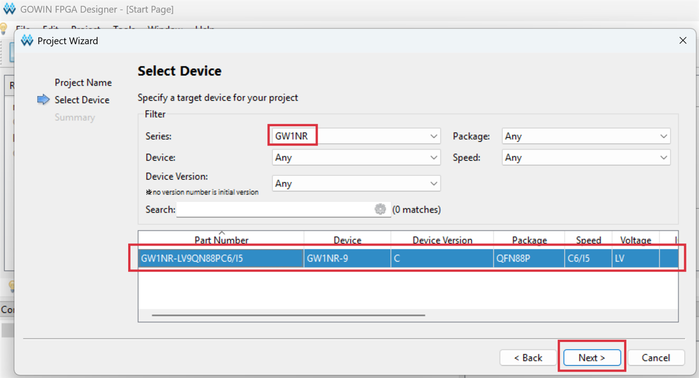
For a first experiment with the Tang Nano, launch the Gowin application, and click File->New->Project. A prompt appears for the device; I decided to target the Tang Nano 9k, and selected the GW1NR series (there's a table in the previous blog post listing which FPGA is in which Tang Nano board). You might need to fill in more parameters until all that’s left is one selection that matches your FPGA, then select it.
The IDE is easy to use. Notice the left pane has Design, Process and Hierarchy tabs underneath it. In the Design tab, it is possible to right-click and add existing or new files. In the Process tab, you can perform actions to ultimately transform those source files all the way through to the final bitstream/bitfile that needs to be transferred to the FPGA.
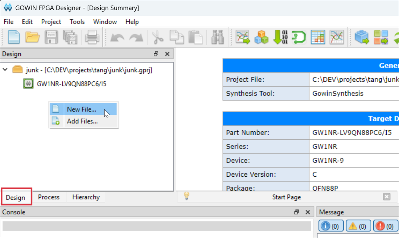
I right-clicked, and selected New File, selected VHDL, and gave it a name of double_blinky (a .vhd suffix will get appended). Double-click on that file in the Design tab, and the text editor pane will appear on the right.
Here is the HDL code I used (I am not a VHDL engineer, so please don’t assume I’m using best practise!). I’ll go through this line-by-line next, but it's best to keep a separate window open with that entire code in view, so it's easier to mentally navigate through it.
Library and Package Declarations
First off, the following is boilerplate and is generally required for VHDL projects. The 1164 refers to an IEEE standard.
library IEEE;use IEEE.STD_LOGIC_1164.ALL;use IEEE.NUMERIC_STD.ALL;
IO Ports List (Entity and Port Declaration)
Like most digital circuits, double_blinky makes use of a clock to progress the circuitry along, and a reset line is very normal too, to make it start in a desired state.
Therefore, double_blinky is expected to have four physical connections to the outside world: clock, reset, and two LED signals. The LED signals can be expressed as a two-bit array (called a vector in VHDL). The entity declaration, including its port list, describes these four input or output signals.
The reset signal is named reset_n just to make it clear that the signal is expected to go low to perform the reset action. This is commonly called an active-low reset.
entity TOP is
    port (
        led : out STD_LOGIC_VECTOR(1 downto 0);
        clk : in STD_LOGIC;
        reset_n : in STD_LOGIC
    );
end TOP;
VHDL Architecture Body
Here's where the FPGA developer gets to type out how they wish the circuit to function!
The architecture has a name, and in this example I've called it RTL. The name can be almost anything you like, but RTL is common. It stands for Register Transfer Level, which basically means describing the circuit in terms of registers and the logic operating between them. This is a very normal way to describe digital circuits intended for implementation in an FPGA.
architecture RTL of TOP is
The architecture body is split into two sections: the declarative region and the statement region. They will both be described next.
Architecture Declaration (Constants and Internal Signals)
These are fairly self-explanatory. Since the clock input may be running at a high speed, a counter is needed. The constants here are used to indicate how many clock pulses are needed before the LED state will be changed:
-- CONSTANTS constant CLK_FREQ_HZ : integer := 27_000_000; constant MSEC_CONST : integer := CLK_FREQ_HZ / 1000; constant LED_DELAY_CONST : integer := MSEC_CONST * 500;
It stands to reason that signals representing the binary count value will be required, and that those signals will probably come from a register, since flip-flops/registers are normally used for anything that needs to remember a state, such as the current counter value.
For that reason I called the signal counter_reg, just to make it clear that the value is stored in a register. Although I've declared it as an integer, the synthesis tool will work out how many bits are needed to implement it in hardware.
Similarly, an internal signal is needed to hold the LED states, so I called it led_reg. This is a two-bit vector, containing the individual bits led_reg(1) and led_reg(0).
-- INTERNAL SIGNALS signal counter_reg : integer range 0 to LED_DELAY_CONST - 1 := 0;
-- LEDs are active-low: '1' = off, '0' = on. -- Start with only the rightmost LED on. signal led_reg : STD_LOGIC_VECTOR(1 downto 0) := "10";
Architecture Statement Region (Concurrent Statements)
Here is where all the meat of the project resides. Unlike conventional software code, which executes instructions sequentially, a different way of thinking is needed with HDL.
All the main statements underneath the following begin keyword are concurrent, meaning they operate alongside one another rather than executing one after the other. When the design is synthesized, these statements describe hardware that operates in parallel within the FPGA.
There are two main elements in this example.
begin
The first element is a concurrent signal assignment, which effectively describes a permanent connection from the internal LED register outputs to the LED output ports declared at the start of the VHDL.
-- Continuously connect the internal LED register outputs to the LED signals led <= led_reg;
The second element is a process statement, often just called a process. A process contains sequential statements, meaning the statements inside it are evaluated in order, unlike the concurrent statements outside it.
The process can be considered to execute whenever one of the signals in its sensitivity list changes. The sensitivity list here contains clk and reset_n.
-- this process will "do something" whenever there is a change on clk or reset_n blinky_process : process(clk, reset_n) begin
The next part follows a common VHDL coding pattern so that the synthesis tool can recognize the developer's intention to create registers with an asynchronous reset.
Here, the reset signal being low will result in counter_reg being cleared, and led_reg being set so that one LED is lit.
The reset is called asynchronous because it doesn't need to wait for a clock edge to take effect.
if reset_n = '0' then -- Asynchronous logic on reset: counter_reg <= 0; -- clear the counter_reg output led_reg <= "10"; -- set the LED register output to a known setting
The next part continues the usual VHDL pattern for describing clocked registers. The rising_edge(clk) function checks for a rising clock edge, and this is one of the patterns the synthesis tool recognizes when deciding to implement flip-flops.
Here, the counter register is compared with a maximum desired count value. If it matches, the counter register is set back to zero.
The LED register is also updated, with its two individual bits swapped around. This is what makes the LEDs alternate from their previous state. The & operator concatenates the bits, joining them together into a new two-bit value.
If the counter register has not reached the maximum desired value, then it is incremented by 1. The updated value will appear after the rising clock edge, once the register has updated.
elsif rising_edge(clk) then -- On every rising edge of the 27 MHz clock -- i.e. every assignment here results in a clocked output, -- i.e. registers. if counter_reg = LED_DELAY_CONST - 1 then -- 500 ms worth of clock cycles have elapsed counter_reg <= 0;
-- Concatenate the two bits in reverse order, -- effectively swapping the two LED states led_reg <= led_reg(0) & led_reg(1);
else counter_reg <= counter_reg + 1; end if; end if; end process;
end RTL;
The final end process; marks the end of the process statement, and end RTL; marks the end of the architecture body.
That's the entire circuit! The counter counts clock pulses, and every 500 milliseconds the LED register swaps its two bits, causing the LEDs to alternate. Because the LEDs are active-low, a zero turns an LED on and a one turns it off.
VHDL Code Summary
Shown below is a diagram to explain/summarize the code. The entity on the left shows the ports that the project uses, i.e. clock and reset inputs, and two LED outputs.
The architecture body describes the circuit's behaviour. Most of the work takes place inside a process, which has an asynchronous reset portion used to initialize the registers, and a clocked portion which does everything else.
The clocked portion increments counter_reg on each rising edge of the clock until it reaches a defined value (LED_DELAY_CONST - 1), at which point the counter is reset to zero. At the same time, the two bits in led_reg are swapped, causing the LEDs to alternate. The led_reg signal represents the outputs of a two-bit register, and a separate concurrent signal assignment connects these to the LED output ports in the TOP entity.

The entity ports need to be connected to physical FPGA pins for this project to be useful, i.e. we need to connect the clock input to a real oscillator, the reset input to a real reset button, and the LED outputs to actual LEDs. That’s next.
Physical Constraints (Pins)
The VHDL source code for the project has been covered, but as you’ve noticed, the actual physical pin numbers were not discussed. That’s because they are placed in a separate file, known as a physical constraints file, or .cst file in Gowin terminology. I’ll cover this further below so don’t do it yet, but just for information, the file can either be created or added from the same Design tab pane as before, by right-clicking and then if you choose New File then you can select Physical Constraints File. Alternatively, it is possible to wait and create the constraints file graphically using a ‘FloorPlanner’.
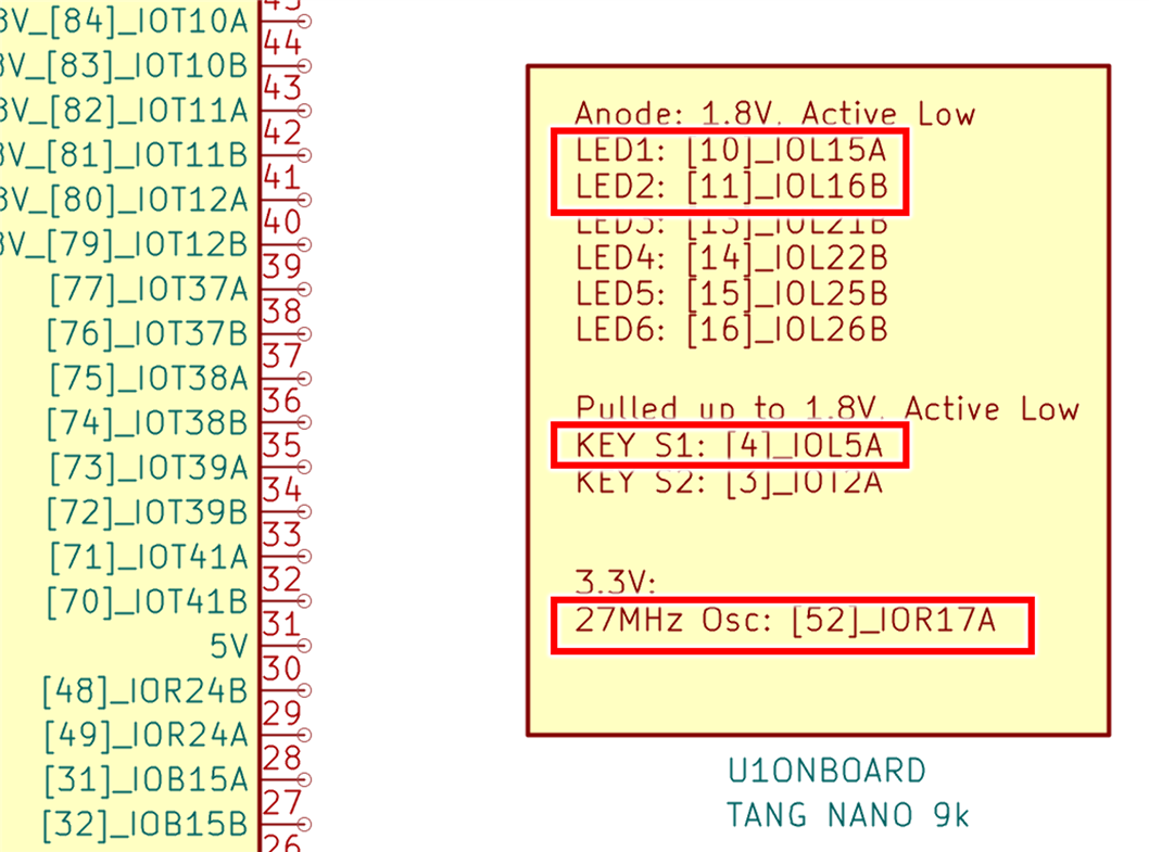
To prepare, you'll need to know which pins you wish to use, so the schematic could be consulted (or see the first blog post). Here you can see that the four connections this project will use are for the two LEDs, the 27 MHz clock, and a push-button for reset. The notation below contains the FPGA physical package pin numbers shown as [n]. They are FPGA pin numbers 10, 11 for LED1, LED2, and pin 4 for button S1, and pin 52 for the LED.
Synthesis
In the Process tab, a list of icons is shown. Double-click on Synthesis (don't click on FloorPlanner yet) and the VHDL compiler will run.
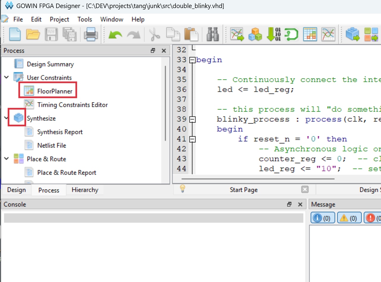
If all went well, the Synthesis icon will change to a green-circled check-mark. Double-click on Synthesis Report if you’re curious.
Now you’re ready to assign pins.
Assigning Pins Constraints using the FloorPlanner
Double-click on FloorPlanner within the User Constraints in the Process pane. If a constraint file does not already exist, one will be created.
The FloorPlanner app window appears, and the right side of it will contain a block diagram showing all the elements that were discussed in the first blog post, such as CFUs, BSRAM and IOBs. This level of detail is not needed for now, so click on the tab above that block diagram, it will be labelled Package View. Zoom in or out if it’s not clear (center mouse wheel, or use View from the top menu drop-down).
Expand the list in the left pane, to see all the Ports (pins) that the project uses, and then you can drag them onto the diagram, to choose which pin you want them to be on.
In the table at the bottom, verify the IO Type matches what is required. In the case of the Tang Nano 9k, from the circuit diagram (see the first blog post), it is clear that the LED anodes are wired to a 1.8V supply, so LVCMOS18 was used. The Pull Mode refers to pullup/pulldown resistors, but they are not needed, so they were set to None (double-click on the text there to see a drop-down appear, and there will be options inside such as PULL UP, PULL DOWN and NONE). Note that the clock is set to LVCMOS33, because, according to the Tang Nano 9k schematic, a 3.3V crystal oscillator is present on the board, wired to pin 52 on the FPGA.

Save and exit from the FloorPlanner once those four port constraints are complete. Now in the Design tab, there will be a constraint file listed. It contains the following text, and it can be manually edited if desired in future:
IO_LOC "led[1]" 11;IO_PORT "led[1]" IO_TYPE=LVCMOS18 PULL_MODE=NONE DRIVE=8 BANK_VCCIO=1.8;IO_LOC "led[0]" 10;IO_PORT "led[0]" IO_TYPE=LVCMOS18 PULL_MODE=NONE DRIVE=8 BANK_VCCIO=1.8;IO_LOC "reset_n" 4;IO_PORT "reset_n" IO_TYPE=LVCMOS18 PULL_MODE=NONE BANK_VCCIO=1.8;IO_LOC "clk" 52;IO_PORT "clk" IO_TYPE=LVCMOS33 PULL_MODE=NONE BANK_VCCIO=3.3;
Timing Constraints
The double-blinky project doesn’t run very fast, but the clock signal could in theory have been even higher than 27 MHz, and at some point the FPGA might configure the internal routing in a fashion that causes issues for high-speed signals. It is best to let the software know what sort of performance is needed.
In the Process tab, double-click on Timing Constraints Editor, and let it create a timing constraints file (.sdc suffix). Expand the port list in the left pane, then right-click on the high speed signal, and click on Add Clock.

In the popup window that appears, fill in the details (enter the frequency and the period will auto-fill) then click OK.
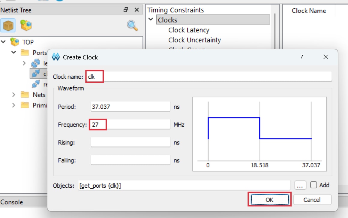
Save the file and exit the constraint editor. Now if you go to the Design tab, a timing constraint file will be listed in the left pane. It should contain the following:
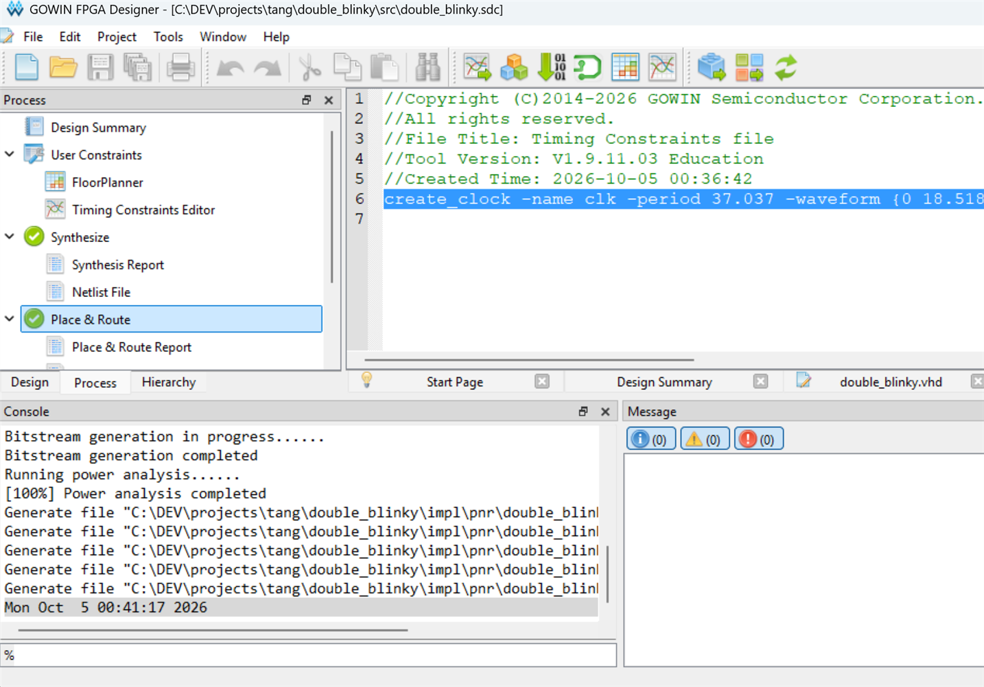
create_clock -name clk -period 37.037 -waveform {0 18.518} [get_ports {clk}]
Place and Route
Back into the Process tab where Synthesis was clicked on earlier, now that the constraint file is also prepared, double-click on Place & Route.
If all goes well, the icon changes to a green circled check-mark.
Programming the Bitfile (Bitstream)
By now, a bitfile will have been generated (a load of files are dumped in the impl/pnr sub-folder by the Gowin software.
To program that into the Tang Nano board, first attach the board using a USB cable (see the important earlier comments about that!). If you want to double-check, in Windows Device Manager, a USB Serial Port should appear under Ports (COM & LPT), and there should also be USB Serial Converter A and USB Serial Converter B, both under Universal Serial Bus Controllers.
From the Process tab, scroll down and below Synthesis and Place & Route, you’ll see a Programmer icon. Double-click it to launch the Gowin Programmer app.
If all goes well, a Cable Setting pop-up will appear. I found that I needed to change the Port from USB Debugger A/0/290 to USB Debugger A/1/289. The 289 seemed important, whereas the number 0 or 1 changed occasionally I believe (but not sure). If I didn’t select the correct choice, then the programming would later hang at zero percent. If you find programming hangs, then try changing that setting.

Click on the icon (highlighted above) to initiate the programming sequence. It will transfer the code to RAM to execute, but if you wish to make it permanent, first double-click just below Operation, where the text SRAM Program is displayed, and then change that to Embedded Flash (if you’re using a Tang Nano board with on-chip flash in the Gowin device).

The bitfile should transfer in a few seconds, and then two LEDs should blink alternately. Pressing the S1 button (it is the top-left button, if the USB cable is to your left) should reset the hardware (since that was where the reset port was attached), and holding it down will keep it in reset, and when released, the LEDs will start alternately blinking again.
Instrumenting with GAO: Gowin Analyzer Oscilloscope
A feature that comes with the development environment is a sort of embedded logic analyzer, that can be added to a project. I decided to try it.
From the Design pane, right-click and select New File, then choose GAO Config File.

In the Wizard popup that appears, I selected Lite for now.

For the GAO setting file name, I appended _debug to the project name.

Next, some more settings appear. I configured those as shown in the screenshot below.

Once I was happy with that, I went to File->Save, to save the changes to that .rao file (GAO Config File).
After that, I went into the Process pane, did a clean Synthesize, followed by a clean Place & Route, and then programmed the board as before. GAO did not work for me using SRAM load, so I selected Flash when programming the device. The LEDs blinked as before, i.e. the VHDL code was running fine.
To connect to the embedded logic analyzer, I went to Tool->Gowin Analyzer Oscilloscope, and selected the same value channel to connect to as I had used for the programmer, which in my case was numbered 289. The logic analyzer pane appeared, and there was a blue icon to start a capture, and a ‘continuous capture’ icon next to that.
The animated GIF here shows what I saw with the continuous capture.

Summary
Several of the Tang Nano boards were introduced in the first blog post. This second blog explored the Gowin software which is needed to build projects and transfer them onto the board.
For creating projects targeting FPGAs such as those on Tang nano boards, the Gowin FPGA Designer software is quite user-friendly, and straightforward to use. It doesn’t take up much space on the PC either (ballpark 2 GB, which is small in FPGA world! Xilinx software takes up tenfold space).
In this blog post, a VHDL project was created from scratch, to make a couple of LEDs perform a double-blinky sequence. The Gowin software was then used to synthesize the design, and graphical tools were used to set the pin and clock constraints, before doing the placement/routing.
The programming went fine, but the Tang Nano boards are quirky in that a normal USB-C-to-C cable might not always work, and I don’t think the supplied USB-A-to-C cables are trustworthy either. Best to use your own known working USB-A-to-C cable.
Finally, the ability to debug hardware in action, using the Gowin Analyzer Oscilloscope (GAO), was briefly explored.
Thanks for reading!