


Polyphase Interpolators
In the previous post we have looked at and important class of FIR filters, namely Polyphase architectures, which are extensively used for changing the sample rate of a signal by and integer factor, a process called interpolation or decimation. We have looked at the particular case where the system clock rate is equal to the lower sample rate, that is the input rate for an interpolator and the output rate for a decimator. In that case, a Polyphase FIR that interpolates or decimates by a factor M consists simply of M individual single rate FIRs running in parallel. We will look now at the more interesting case when the system clock rate is equal to the larger of the two sample rates and we will start with the interpolator.
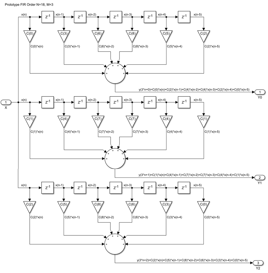
Here is again what needs to be computed, exemplified by a 3-phase interpolator with a prototype single rate FIR of order N=18:
If the input sample rate is M times smaller than the system clock frequency and the output sample rate, it is possible to compute all M branches with the same hardware sequentially, one output sample at a time, using only N/M multipliers instead of the original N. Every M clocks a new input sample is fed into the filter and then the M outputs are computed. It is obvious that we can replace the M input delay lines with a common one, since they all contain exactly the same data and we can also reuse the multipliers and the post adder as long as we change the set of coefficients used every clock. So this is how a design that uses time division multiplexing to implement all M phases with a single set of multipliers and adders would look like:

The red blocks and wires indicate activity at the fast output sample rate, which is also equal to the system clock rate, while the green blocks and wires correspond to M times lower input sample rate. We have a new input in the fast clock domain called VI to show when a new input sample arrives, it should be active once every M clocks. This signal acts as a clock enable for the input shift registers, so that they can also run at the same system clock frequency and we are emulating the lower sample rate clock domain using this clock enable mechanism. While the FPGA fabric can easily implement multi-clock designs, the DSP48 primitive has only one clock input, but every internal register has its own independent clock enable and synchronous reset, so if we want to be able to map these registers into the DSP48s we have to use this clock enable technique and keep the entire FIR as a single clock design.The coefficients for each one of the M branches of the filter are held in ROM tables, which are M locations deep, each one addressed by a counter. The counters will count from 0 to M-1 and are monostable ones. They stay in the zero state until a pulse arrives on the VI input port, when they start counting. When they reach M-1 they revert to 0 and stop, unless a new VI pulse arrives at that exact moment in time, which is normally the case unless we want to implement some kind of input flow control and run the filter at an input sample rate lower than the system clock frequency divided by M. We will of course want to pipeline this new design, which is why I have also added the transversal and longitudinal pipeline cuts necessary. All wires cross these cuts in the same direction, so we need to add one register level for every crossing. This gets us the final implementation:

All the resources that go into DSP48s, registers, multipliers and adders, have a colored background, with a different color for every DSP48 primitive in the chain. The blocks with a white background will be fabric based, essentially the coefficient ROMs and the counters driving their address inputs. A thing to note is that the registers labeled AREG1 have a clock enable and run at an effective clock rate that is M times slower than the rest of the design, although there is of course just one single system clock.
This Polyphase FIR implementation is not much different from a simple single rate FIR one. Instead of a single fixed set of coefficients we have now M sets, stored in external ROMs and every second register in the input delay line has a clock enable and operates once every M clocks. This is a very efficient implementation, scalable to any filter size and able to maintain the highest possible clock rate.
In the next post we will look at the dual architecture of this filter, the M-phase decimator.
Back to the top: The Art of FPGA Design Season 2