


Polyphase Decimators
The Polyphase Decimator FIR is the dual structure of the Polyphase Interpolator. The basic idea is that you can reduce the sample rate of a signal by a factor of M if you keep only one out of every M samples. This only works if the signal being decimated has a limited bandwidth, otherwise we will get aliasing artifacts. This is achieved by low-pass filtering the input signal before decimation, with a prototype filter which is very similar to the one we encountered in the interpolation case. The efficient implementation comes from the fact that we do not need to compute the output samples that will be dropped, which reduces the amount of calculations by a factor of M. This is done using the same polyphase decomposition of the prototype filter into M branches. The decimator accepts M input samples every clock and applies each one to one of the filter branches. The outputs of the M FIR branches are then added together, and this produces one output sample every clock. Conceptually this would look like this:
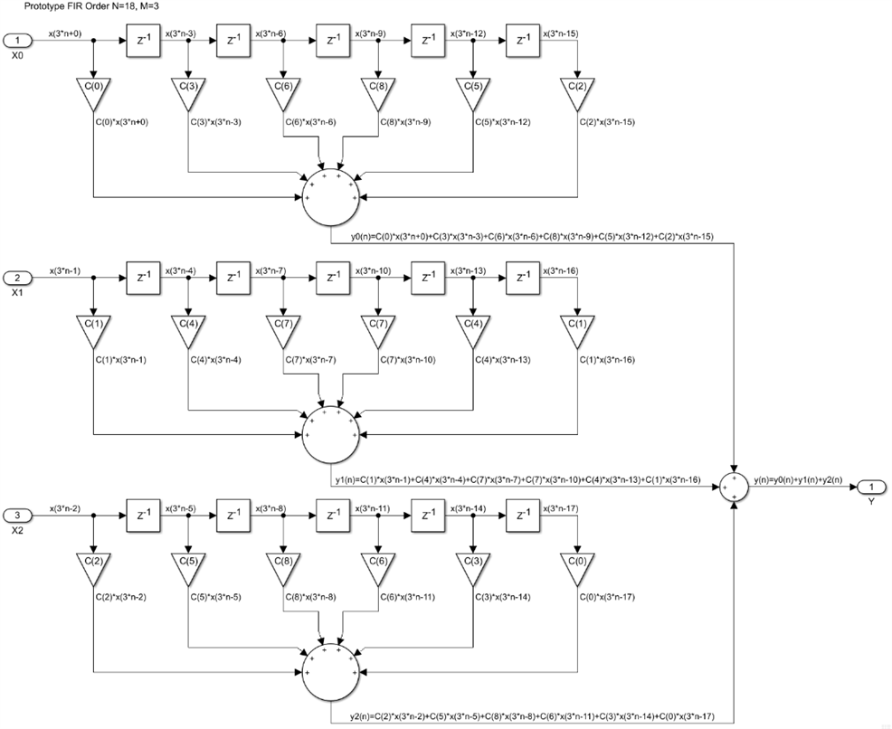
Implementing this is pretty straightforward, M single rate FIRs, each one with N/M taps. This requires N multiplications, which is the order of the prototype filter. The question is how would we implement this algorithm when the clock rate is equal to the input sample rate, when the design will accept one input sample every clock and produce one output sample every M clocks. We would like to use a single chain of N/M multipliers and adders, which would in turn implement all M branches of the filter in M clocks. This is a multi-channel version of a single rate FIR, which can always be achieved by replacing every delay in the filter with M delays, then storing M sets of filter coefficients into ROM tables and use a different set every clock:

I replaced the M/N input adders with an adder chain and the final M-input adder with an accumulator. The VI input is active high once every M clocks and it is used to synchronize the counters driving the ROM coefficient tables. As VO, it also indicates when a new output sample is available.
This particular implementation of a polyphase decimator is widely used, but it has a number of drawbacks. First, it uses one extra DSP48 for the output accumulator, so the design uses N/M+1 instead of just N/M. The input delay line will consist of M-clock delays, actually M+1 clocks after we do the transversal pipeline cuts. Since a DSP48 has only 2 AREG registers, any polyphase FIR decimator implemented this way, even with M=2, will have to use fabric based delays. There is however a better way to build a polyphase decimator FIR using DSP48s. The decimator is the dual structure of the interpolator in a way similar to direct and transpose architectures of a single rate FIR. So let's convert all the M polyphase branches from a direct to a transpose implementation:
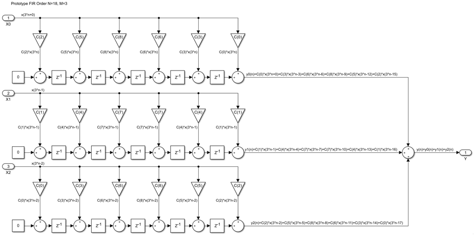
Note that the delays are on the output path rather than the input, and the order of the coefficients for each branch is flipped. This transposed dual version is functionally equivalent to the direct implementation in the first picture of this post. But this alternate structure leads to a very different resource time sharing between the M paths. Instead of having one final accumulator, it is possible to distribute it along the output path, which is now a chain of accumulators, rather than a chain of adders:

Each accumulator in the chain adds M partial products, then passes the result every M clocks to the next accumulator, which adds another M partial products, until one final output sample is produced every M clocks. This is a much better structure compared with the previous one because it uses N/M delays instead of N delays and there is no need for a final DSP48 to add the outputs of all the M branches. Pipelining the design to achieve full speed is easy, we need three longitudinal pipeline cuts, which leads to this final implementation:

All the resources that are internal to DSP48s are colored, with a different color for every DSP48. The blocks with a white background will be fabric based, in this case only the registered ROM coefficient tables and their address counters. Like all transposed implementations, this is not really scalable, because of the high fanout of the X and VI signals, there is a chain size from which the speed will start to drop, typically around 20 DSP48s. However, this is not a problem. Like it was the case for other transposed FIRs, we can add transversal pipeline cuts every 20 taps or so and still achieve the highest possible speed. Finally, like other transposed FIRs, this design has very low latency, in this case M+3 clocks.
In the next post we will try to see if it is possible to take advantage of the prototype filter symmetry in the case of polyphase interpolating and decimating FIRs.
Back to the top: The Art of FPGA Design Season 2