element14 Community
element14 Community
    Register Log In
  • Site
  • Search
  • Log In Register
  • About Us
  • Community Hub
    Community Hub
    • What's New on element14
    • Feedback and Support
    • Benefits of Membership
    • Personal Blogs
    • Members Area
    • Achievement Levels
  • Learn
    Learn
    • Ask an Expert
    • eBooks
    • element14 presents
    • Learning Center
    • Tech Spotlight
    • STEM Academy
    • Webinars, Training and Events
    • Learning Groups
  • Technologies
    Technologies
    • 3D Printing
    • FPGA
    • Industrial Automation
    • Internet of Things
    • Power & Energy
    • Sensors
    • Technology Groups
  • Challenges & Projects
    Challenges & Projects
    • Design Challenges
    • element14 presents Projects
    • Project14
    • Arduino Projects
    • Raspberry Pi Projects
    • Project Groups
  • Products
    Products
    • Arduino
    • Avnet Boards Community
    • Dev Tools
    • Manufacturers
    • Multicomp Pro
    • Product Groups
    • Raspberry Pi
    • RoadTests & Reviews
  • Store
    Store
    • Visit Your Store
    • Choose another store...
      • Europe
      •  Austria (German)
      •  Belgium (Dutch, French)
      •  Bulgaria (Bulgarian)
      •  Czech Republic (Czech)
      •  Denmark (Danish)
      •  Estonia (Estonian)
      •  Finland (Finnish)
      •  France (French)
      •  Germany (German)
      •  Hungary (Hungarian)
      •  Ireland
      •  Israel
      •  Italy (Italian)
      •  Latvia (Latvian)
      •  
      •  Lithuania (Lithuanian)
      •  Netherlands (Dutch)
      •  Norway (Norwegian)
      •  Poland (Polish)
      •  Portugal (Portuguese)
      •  Romania (Romanian)
      •  Russia (Russian)
      •  Slovakia (Slovak)
      •  Slovenia (Slovenian)
      •  Spain (Spanish)
      •  Sweden (Swedish)
      •  Switzerland(German, French)
      •  Turkey (Turkish)
      •  United Kingdom
      • Asia Pacific
      •  Australia
      •  China
      •  Hong Kong
      •  India
      •  Korea (Korean)
      •  Malaysia
      •  New Zealand
      •  Philippines
      •  Singapore
      •  Taiwan
      •  Thailand (Thai)
      • Americas
      •  Brazil (Portuguese)
      •  Canada
      •  Mexico (Spanish)
      •  United States
      Can't find the country/region you're looking for? Visit our export site or find a local distributor.
  • Translate
  • Profile
  • Settings
FPGA
  • Technologies
  • More
FPGA
Forum Neo Geo Pocket Color Video Out (DAC/FPGA)
  • Blog
  • Forum
  • Documents
  • Quiz
  • Events
  • Polls
  • Files
  • Members
  • Mentions
  • Sub-Groups
  • Tags
  • More
  • Cancel
  • New
Join FPGA to participate - click to join for free!
Actions
  • Share
  • More
  • Cancel
Forum Thread Details
  • State Suggested Answer
  • Replies 19 replies
  • Answers 11 answers
  • Subscribers 551 subscribers
  • Views 4349 views
  • Users 0 members are here
  • retro gaming
  • dac
  • fpga
  • digital-to analog converter
  • video games
Related

Neo Geo Pocket Color Video Out (DAC/FPGA)

kragit
kragit over 8 years ago

Hi everyone!


Looking to achieve RGB analog video out on a Neo Geo Pocket Color. No known mods currently exist for this. There are single digit K2_VIDEOs out in the wild that achieve this, but I believe these were made by SNK themselves for internal use only. Other people have apparently gotten video out with FPGAs, but no one has publicly documented it.


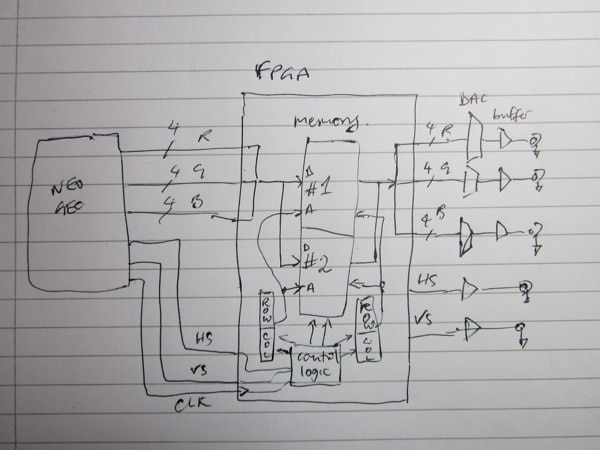
Here are the LCD signals as printed on the board & additional information from someone who's apparently achieved this:


I've done it with a small FPGA. The LCD signals can't be simpler: R0~3 is 4bit red, G0~3 is 4bit green, B0~3 is 4bit blue, DOTCLK is the pixel clock, SPL is horizontal sync, SPS is frame sync.
[...]
It can't be done by just wiring a scart cable to the board, you have to buffer and convert the color data from the NGPC, then do digital to analog conversion if you want analog RGB output.


I'm venturing into the FPGA scene for this with no past experience with FPGAs and a rudimentary understanding of digital electronics (I can follow guides, solder, etc. I built a CMVS this way).


Any help would be appreciated. Thanks!

  • Sign in to reply
  • Cancel

Top Replies

  • johnbeetem
    johnbeetem over 8 years ago in reply to kragit +4 suggested
    Adam Kragt wrote: Appreciate the info! The biggest thing is just trying to figure out where to start as a total beginner. With FPGAs, start by copying a tutorial design exactly. FPGA tools have a steep…
  • jc2048
    jc2048 over 8 years ago +3 suggested
    You might consider applying for this roadtest https://www.element14.com/community/roadTests/1796/l/Terasic-P0082-DE0-Nano-FPGA-Development-Kit That would get you some kit to use and an opportunity to learn…
  • johnbeetem
    johnbeetem over 8 years ago +3 suggested
    These are general comments about FPGAs and VGA output and probably not all that helpful for the NPGC, but here goes anyway. There are a number of FPGA boards out there that support VGA graphics, and some…
Parents
  • jc2048
    0 jc2048 over 8 years ago

    As to the design itself, this would be my first go at a system block diagram based on what you've said so far


    image


    Here the LCD data gets latched into the FPGA and stored in row/column sequence in an internal memory. Unless you know the two sides won't run past each other, you'd use a pair of buffers, writing to one and reading from the other. You'd then pick it out of the memory at the appropriate times to fit with the output syncs that you'd generate. The colour outputs would then go to video rate DACs [Digital to Analogue Converters]. Sometimes converters can drive cables, but if not you'd need video buffers to do it. The syncs might manage with a logic line-driver (depends what the display is - that would work with VGA, but not necessarily with other analogue monitors). You have to work out how you would get the appropriate output syncs from the LCD clock. You'll find everything simpler if you can lock the output to the LCD signals so that input and output sides are timing related to each other [perhaps by multiplying the LCD clock, since it sounds like the output will have to run on a higher clock rate].


    The DACs and cable drivers would be best on a pcb [they'll need careful layout]. Since it's only 4-bits for each of the colours, it's possible that you might get away with something quick-and-dirty like using resistors followed by a buffer to make your own DAC. Might be worth a try, though don't pin your hopes on it.


    First step, if you're serious about this, is to determine the timing of the LCD drive. You need to sketch out the sync timing, orientation, blanking periods and number of pixels. Then you need to decide what output display you'd use and its capabilities [as in what mode you'd use it in and whether it could work in a way that related well to the LCD]. Then you'd need to consider how you'd piece together a prototype and then start work on the design of the FPGA.


    There's no reason why you couldn't do all that, but it's quite an involved project to do from a standing start if you haven't done any of that before. Do you have any experience with designing with logic chips? If you could do a design for this with CMOS logic and an SRAM, then you could certainly manage the FPGA design [since 'coding' an FPGA is really a disguised way of doing logic design], but if you come from a coding background you would find it more difficult since you'd be learning to do logic design. Unlike processor coding, FPGAs are best programmed with the underlying hardware very much in mind [perhaps think of it like doing very low level assembly programming, with timing so critical that you're counting processor cycles, and with multiple threads all executing simultaneously and having to interact with each other]. It's not as difficult as I make it sound, but you do need a somewhat different mindset from processor coding.


    If you're unsure, I'd encourage you to go for the roadtest and (if you were successful) work through the Altera teaching material. That way you'd find out if you were suited to FPGA design and you'd have a nice development board to work with that could easily cope with what you want to do here.

    • Cancel
    • Vote Up +1 Vote Down
    • Sign in to reply
    • Verify Answer
    • Reject Answer
    • Cancel
Reply
  • jc2048
    0 jc2048 over 8 years ago

    As to the design itself, this would be my first go at a system block diagram based on what you've said so far


    image


    Here the LCD data gets latched into the FPGA and stored in row/column sequence in an internal memory. Unless you know the two sides won't run past each other, you'd use a pair of buffers, writing to one and reading from the other. You'd then pick it out of the memory at the appropriate times to fit with the output syncs that you'd generate. The colour outputs would then go to video rate DACs [Digital to Analogue Converters]. Sometimes converters can drive cables, but if not you'd need video buffers to do it. The syncs might manage with a logic line-driver (depends what the display is - that would work with VGA, but not necessarily with other analogue monitors). You have to work out how you would get the appropriate output syncs from the LCD clock. You'll find everything simpler if you can lock the output to the LCD signals so that input and output sides are timing related to each other [perhaps by multiplying the LCD clock, since it sounds like the output will have to run on a higher clock rate].


    The DACs and cable drivers would be best on a pcb [they'll need careful layout]. Since it's only 4-bits for each of the colours, it's possible that you might get away with something quick-and-dirty like using resistors followed by a buffer to make your own DAC. Might be worth a try, though don't pin your hopes on it.


    First step, if you're serious about this, is to determine the timing of the LCD drive. You need to sketch out the sync timing, orientation, blanking periods and number of pixels. Then you need to decide what output display you'd use and its capabilities [as in what mode you'd use it in and whether it could work in a way that related well to the LCD]. Then you'd need to consider how you'd piece together a prototype and then start work on the design of the FPGA.


    There's no reason why you couldn't do all that, but it's quite an involved project to do from a standing start if you haven't done any of that before. Do you have any experience with designing with logic chips? If you could do a design for this with CMOS logic and an SRAM, then you could certainly manage the FPGA design [since 'coding' an FPGA is really a disguised way of doing logic design], but if you come from a coding background you would find it more difficult since you'd be learning to do logic design. Unlike processor coding, FPGAs are best programmed with the underlying hardware very much in mind [perhaps think of it like doing very low level assembly programming, with timing so critical that you're counting processor cycles, and with multiple threads all executing simultaneously and having to interact with each other]. It's not as difficult as I make it sound, but you do need a somewhat different mindset from processor coding.


    If you're unsure, I'd encourage you to go for the roadtest and (if you were successful) work through the Altera teaching material. That way you'd find out if you were suited to FPGA design and you'd have a nice development board to work with that could easily cope with what you want to do here.

    • Cancel
    • Vote Up +1 Vote Down
    • Sign in to reply
    • Verify Answer
    • Reject Answer
    • Cancel
Children
  • kragit
    0 kragit over 8 years ago in reply to jc2048

    A lot to digest!

    Do you have any experience with designing with logic chips?

    Nope! Very green to pretty much every aspect of this. My experience consists of being a web dev and knowing how to solder smaller electronics (working on a Consolized MVS system and installing (soldering) a 3DS capture board for the same person I'm trying to figure out the NGPC capture for).


    I have tried to read/watch some FPGA documentation in the past, though I still didn't quite understand things.


    Hoping there might be something out there that would be easy enough to setup/program that I could muddle through it. Essentially 'baby's first FPGA' :-P

    • Cancel
    • Vote Up +1 Vote Down
    • Sign in to reply
    • Verify Answer
    • Cancel
element14 Community

element14 is the first online community specifically for engineers. Connect with your peers and get expert answers to your questions.

  • Members
  • Learn
  • Technologies
  • Challenges & Projects
  • Products
  • Store
  • About Us
  • Feedback & Support
  • FAQs
  • Terms of Use
  • Privacy Policy
  • Legal and Copyright Notices
  • Sitemap
  • Cookies

An Avnet Company © 2025 Premier Farnell Limited. All Rights Reserved.

Premier Farnell Ltd, registered in England and Wales (no 00876412), registered office: Farnell House, Forge Lane, Leeds LS12 2NE.

ICP 备案号 10220084.

Follow element14

  • X
  • Facebook
  • linkedin
  • YouTube