element14 Community
element14 Community
    Register Log In
  • Site
  • Search
  • Log In Register
  • Community Hub
    Community Hub
    • What's New on element14
    • Feedback and Support
    • Benefits of Membership
    • Personal Blogs
    • Members Area
    • Achievement Levels
  • Learn
    Learn
    • Ask an Expert
    • eBooks
    • element14 presents
    • Learning Center
    • Tech Spotlight
    • STEM Academy
    • Webinars, Training and Events
    • Learning Groups
  • Technologies
    Technologies
    • 3D Printing
    • FPGA
    • Industrial Automation
    • Internet of Things
    • Power & Energy
    • Sensors
    • Technology Groups
  • Challenges & Projects
    Challenges & Projects
    • Design Challenges
    • element14 presents Projects
    • Project14
    • Arduino Projects
    • Raspberry Pi Projects
    • Project Groups
  • Products
    Products
    • Arduino
    • Avnet Boards Community
    • Dev Tools
    • Manufacturers
    • Multicomp Pro
    • Product Groups
    • Raspberry Pi
    • RoadTests & Reviews
  • Store
    Store
    • Visit Your Store
    • Choose another store...
      • Europe
      •  Austria (German)
      •  Belgium (Dutch, French)
      •  Bulgaria (Bulgarian)
      •  Czech Republic (Czech)
      •  Denmark (Danish)
      •  Estonia (Estonian)
      •  Finland (Finnish)
      •  France (French)
      •  Germany (German)
      •  Hungary (Hungarian)
      •  Ireland
      •  Israel
      •  Italy (Italian)
      •  Latvia (Latvian)
      •  
      •  Lithuania (Lithuanian)
      •  Netherlands (Dutch)
      •  Norway (Norwegian)
      •  Poland (Polish)
      •  Portugal (Portuguese)
      •  Romania (Romanian)
      •  Russia (Russian)
      •  Slovakia (Slovak)
      •  Slovenia (Slovenian)
      •  Spain (Spanish)
      •  Sweden (Swedish)
      •  Switzerland(German, French)
      •  Turkey (Turkish)
      •  United Kingdom
      • Asia Pacific
      •  Australia
      •  China
      •  Hong Kong
      •  India
      •  Korea (Korean)
      •  Malaysia
      •  New Zealand
      •  Philippines
      •  Singapore
      •  Taiwan
      •  Thailand (Thai)
      • Americas
      •  Brazil (Portuguese)
      •  Canada
      •  Mexico (Spanish)
      •  United States
      Can't find the country/region you're looking for? Visit our export site or find a local distributor.
  • Translate
  • Profile
  • Settings
FPGA
  • Technologies
  • More
FPGA
Forum What is the thick lines indicate and thin lines indicate in below picture?
  • Blog
  • Forum
  • Documents
  • Quiz
  • Events
  • Polls
  • Files
  • Members
  • Mentions
  • Sub-Groups
  • Tags
  • More
  • Cancel
  • New
Join FPGA to participate - click to join for free!
Actions
  • Share
  • More
  • Cancel
Forum Thread Details
  • State Verified Answer
  • Replies 5 replies
  • Answers 1 answer
  • Subscribers 535 subscribers
  • Views 1553 views
  • Users 0 members are here
  • fpga
Related

What is the thick lines indicate and thin lines indicate in below picture?

krishna_teja
krishna_teja over 3 years ago

Is that the trace width or something else?

Attachments:
image
  • Sign in to reply
  • Cancel

Top Replies

  • shabaz
    shabaz over 3 years ago +3 verified
    Hi Krishna. They are most likely signal and power traces (the power traces being the thicker ones). The specific part datasheet will indicate what those pads represent, but the thick traces look destined…
  • shabaz
    shabaz over 3 years ago in reply to krishna_teja +2 suggested
    Hi Krishna, In general but especially in this case you'd need to follow the datasheet, it's likely prescriptive in that area unless you wish to experiment and affect manufacturability/reliability etc …
  • krishna_teja
    krishna_teja over 3 years ago in reply to shabaz +1
    How much width should be the power traces be? Is there only the change in trace width or something else? So the thinner ones would be smaller trace width compared to the thicker one. Am I right sir?
  • shabaz
    0 shabaz over 3 years ago

    Hi Krishna.


    They are most likely signal and power traces (the power traces being the thicker ones).

    The specific part datasheet will indicate what those pads represent, but the thick traces look destined for the power plane(s).

    • Cancel
    • Vote Up +3 Vote Down
    • Sign in to reply
    • Verify Answer
    • Reject Answer
    • Cancel
  • krishna_teja
    0 krishna_teja over 3 years ago in reply to shabaz

    How much width should be the power traces be? Is there only the change in trace width or something else? So the thinner ones would be smaller trace width compared to the thicker one. Am I right sir?

    • Cancel
    • Vote Up +1 Vote Down
    • Sign in to reply
    • Verify Answer
    • Cancel
  • shabaz
    0 shabaz over 3 years ago in reply to krishna_teja

    Hi Krishna,


    In general but especially in this case you'd need to follow the datasheet, it's likely prescriptive in that area unless you wish to experiment and affect manufacturability/reliability etc (and probably you don't since these parts are expensive). And then in production it may need to be tweaked further, but the datasheet would be the starting point.

    • Cancel
    • Vote Up +2 Vote Down
    • Sign in to reply
    • Verify Answer
    • Reject Answer
    • Cancel
  • krishna_teja
    0 krishna_teja over 3 years ago in reply to shabaz

    image


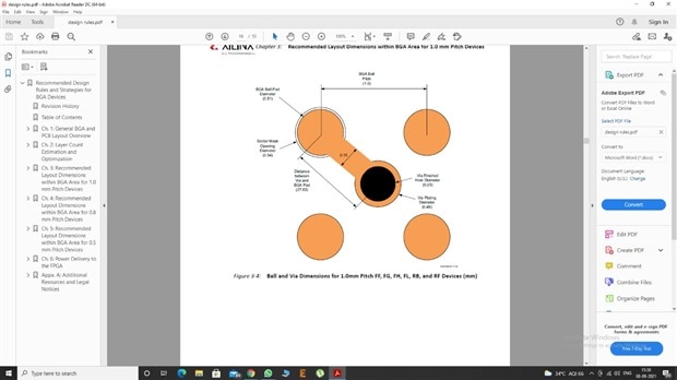
    So, in this image, the width of the trace is given as 0.15mm(6mils). Here should I follow this trace width for power traces? For the thinner one what trace width should I follow?

    • Cancel
    • Vote Up +1 Vote Down
    • Sign in to reply
    • Verify Answer
    • Cancel
  • shabaz
    0 shabaz over 3 years ago in reply to krishna_teja

    Hi Krishna,


    The documentation needs to be followed to the fraction of a mil, unless you've got other knowledge about your particular PCB processes that you need to follow (some orgs will have their own guidelines from the manufacturing requirements they need to follow, so you'd need to check in your organisation).

    It's best to read the entire doc, since it's critical, and also you could download Gerber files for any reference design for that chip/package (or ask the manufacturer for these) and examine the measurements using any Gerber viewer. This applies to power and signal traces at the chip, and then beyond that you'd need to follow the signal trace requirements for whatever signal standard you're following etc.

    • Cancel
    • Vote Up +1 Vote Down
    • Sign in to reply
    • Verify Answer
    • Cancel
element14 Community

element14 is the first online community specifically for engineers. Connect with your peers and get expert answers to your questions.

  • Members
  • Learn
  • Technologies
  • Challenges & Projects
  • Products
  • Store
  • About Us
  • Feedback & Support
  • FAQs
  • Terms of Use
  • Privacy Policy
  • Legal and Copyright Notices
  • Sitemap
  • Cookies

An Avnet Company © 2025 Premier Farnell Limited. All Rights Reserved.

Premier Farnell Ltd, registered in England and Wales (no 00876412), registered office: Farnell House, Forge Lane, Leeds LS12 2NE.

ICP 备案号 10220084.

Follow element14

  • X
  • Facebook
  • linkedin
  • YouTube