A 48V DC power bus is common in industrial environments. That voltage often needs to be converted to other levels.
For high-performance processors, FPGAs and application specific ICs, this can be as low as 0.5V or 1V, with a current draw of many amps.
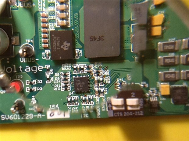
The evaluation kit here (LMG5200POLEVM-10), that I got for review from TI almost a year ago, is intended for such applications - located close to the low voltage load.
GaN Power Stages
This isn't the simplest circuit. It consists of a half-bridge Buck converter, a transormer (a funny one) an output rectifier with filtering.
Primary Side
source: Using the LMG5200POLEVM-10 48V to Point of Load EVM
The half-bridge on the primary side is a GAN device that I've extensively reviewed in previous blogs: LMG5200. Check the blogs for details.
For this design, it's essential to understand that it is used as a typical Buck and that it switches at high frequencies.
We'll visit this component again when we check the PWM controller (it's a smart one with i2c interface) that is the brain of the converter.
Transformer
It's built from PCB traces, with a ferrite core over it. SO no wires in this transformer , just a single PCB trace on each side of the board.
edit: This is a 10 layer board. The Transformer has a 5:1 ratio. Check the comments below.
Planar transformer surrounded by a ferrite core (two half cores that connect trough rectangular openings in the PCB) | 10 layer board with 5 primary windings and 1 secondary winding |
|---|---|
 | Layers 1,4,5,7,10 dedicated to the secondary side (each one turn in parallel) and the other to the primary side (one turn each in series).
The stacking goes S PP SS P S PP S (S=secondary P= primary).
|
source: Using the LMG5200POLEVM-10 48V to Point of Load EVM
It's crazy that you can transfer 75 Watt with this construct, isn't it?
Secondary side
This is a GaN transistor based rectifier and an LC filter to smoothen the output.
The gates of these transistors (in reality Q3 and Q4 in Figure 1 each are constructed with two discrete GaN FETs) are driven with the same signal that drives Q1 and Q2 on the primary side.
Core of the power circuit. Additional decoupling and filter caps not shown here.
source: Using the LMG5200POLEVM-10 48V to Point of Load EVM
There's no heat sink required. When the output current exceeds 20A, active cooling (a fan) is needed.
In the next blogs, I'll check out additional circuits on the development kit: the step-down controller and the on-board 10A pulsing(!) test load.
I hope that someone with sound electromagnetic knowledge chimes in to discuss the PCB transfo (the core is ER18-3.2-10-3F45-S from Ferroxcube).
| Blog Posts |
|---|
| part 1: Design Overview |
| part 2: Current Doubler |
| part 3: Dynamic Test Load |
| Related Blog |
| Checking Out GaN Half-Bridge Power Stage: Texas Instruments LMG5200 - Part 1: Preview |


Top Comments
-

jc2048
-
Cancel
-
Vote Up
+3
Vote Down
-
-
Sign in to reply
-
More
-
Cancel
-

jc2048
in reply to jc2048
-
Cancel
-
Vote Up
+2
Vote Down
-
-
Sign in to reply
-
More
-
Cancel
Comment-

jc2048
in reply to jc2048
-
Cancel
-
Vote Up
+2
Vote Down
-
-
Sign in to reply
-
More
-
Cancel
Children