element14 Community
element14 Community
    Register Log In
  • Site
  • Search
  • Log In Register
  • Community Hub
    Community Hub
    • What's New on element14
    • Feedback and Support
    • Benefits of Membership
    • Personal Blogs
    • Members Area
    • Achievement Levels
  • Learn
    Learn
    • Ask an Expert
    • eBooks
    • element14 presents
    • Learning Center
    • Tech Spotlight
    • STEM Academy
    • Webinars, Training and Events
    • Learning Groups
  • Technologies
    Technologies
    • 3D Printing
    • FPGA
    • Industrial Automation
    • Internet of Things
    • Power & Energy
    • Sensors
    • Technology Groups
  • Challenges & Projects
    Challenges & Projects
    • Design Challenges
    • element14 presents Projects
    • Project14
    • Arduino Projects
    • Raspberry Pi Projects
    • Project Groups
  • Products
    Products
    • Arduino
    • Avnet & Tria Boards Community
    • Dev Tools
    • Manufacturers
    • Multicomp Pro
    • Product Groups
    • Raspberry Pi
    • RoadTests & Reviews
  • About Us
    About the element14 Community
  • Store
    Store
    • Visit Your Store
    • Choose another store...
      • Europe
      •  Austria (German)
      •  Belgium (Dutch, French)
      •  Bulgaria (Bulgarian)
      •  Czech Republic (Czech)
      •  Denmark (Danish)
      •  Estonia (Estonian)
      •  Finland (Finnish)
      •  France (French)
      •  Germany (German)
      •  Hungary (Hungarian)
      •  Ireland
      •  Israel
      •  Italy (Italian)
      •  Latvia (Latvian)
      •  
      •  Lithuania (Lithuanian)
      •  Netherlands (Dutch)
      •  Norway (Norwegian)
      •  Poland (Polish)
      •  Portugal (Portuguese)
      •  Romania (Romanian)
      •  Russia (Russian)
      •  Slovakia (Slovak)
      •  Slovenia (Slovenian)
      •  Spain (Spanish)
      •  Sweden (Swedish)
      •  Switzerland(German, French)
      •  Turkey (Turkish)
      •  United Kingdom
      • Asia Pacific
      •  Australia
      •  China
      •  Hong Kong
      •  India
      •  Japan
      •  Korea (Korean)
      •  Malaysia
      •  New Zealand
      •  Philippines
      •  Singapore
      •  Taiwan
      •  Thailand (Thai)
      •  Vietnam
      • Americas
      •  Brazil (Portuguese)
      •  Canada
      •  Mexico (Spanish)
      •  United States
      Can't find the country/region you're looking for? Visit our export site or find a local distributor.
  • Translate
  • Profile
  • Settings
Test & Tools
  • Technologies
  • More
Test & Tools
Blog Complete Analogue DC Load (0-5A, 0 - 60V) but not 300W :)
  • Blog
  • Forum
  • Documents
  • Files
  • Members
  • Mentions
  • Sub-Groups
  • Tags
  • More
  • Cancel
  • New
Join Test & Tools to participate - click to join for free!
  • Share
  • More
  • Cancel
Group Actions
  • Group RSS
  • More
  • Cancel
Engagement
  • Author Author: Robert Peter Oakes
  • Date Created: 31 Jul 2015 1:37 AM Date Created
  • Views 10074 views
  • Likes 10 likes
  • Comments 43 comments
  • mosfets
  • test_equipment
  • opamps
  • electronic_dc_load
  • testequipment
  • dc_load
Related
Recommended

Complete Analogue DC Load (0-5A, 0 - 60V) but not 300W :)

Robert Peter Oakes
Robert Peter Oakes
31 Jul 2015

image


I have been slowly working through a series of projects and tutorials to share and teach how to use various components and how these can be applied to a Home / Lab power supply, DC Load and the likes.


In order to have our first complete tool, I have completed a DC Load to the above specifications and here are the schematics, and pictures in support of the build


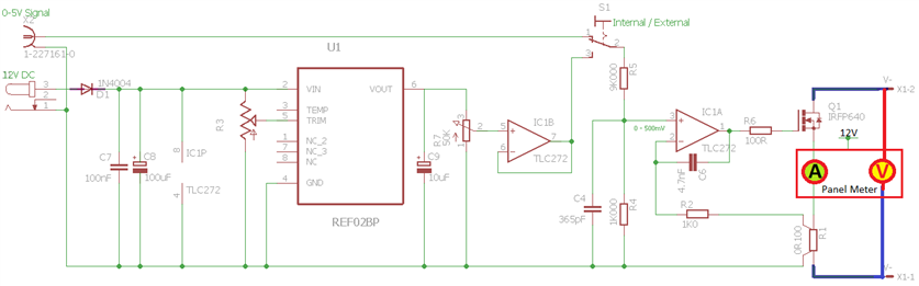
First up the schematic

image

Adhering to the classic, It contains a 5V reference IC and a Dual Op-Amp, most of the schematic should be readily identifiable but I will point out a few things. The DC load will also handle input from an Arbitrary Waveform Generator (0-5V representing 0-5A) and up to about a 2 - 3 KHz square wave if you so desire. It also has a transient response time better than 100uS.


C4 (365pf) and C6 (4.7nF) are required to minimize or prevent oscillations in the control and believe me it will oscillate without C6 and quite badly, see the videos below regarding this


Here is the initial post Electronic DC Load - Design and Build to test PSU Project and a performance tuning video here:- Electronic DC Load - Performance Improvements


The schematics in those posts contained a slight error in the trimmer connection for the VREF, I had it between the supplies rather than the output and Gnd. The above schematic has this corrected.


The values of R4 and R5 are dependent on how accurate you want this to be with respect to a known input or the output of the 5V VREF. The more accurate or more correctly stated, the closer they are to a 10:1 ratio the more closely the DC load will track 0-5V to a 0-5A load.


For me in this build I ultimately went with "close enough" rather than using my precision Vishay resistors. The reason for this is I placed a panel meter on the output (After I hacked it image ) to show me volts and current, and it is only manually adjustable so 0.05% resistors would be a waste. I will be building another automated version in the future and this will be far more precise so stay tuned image


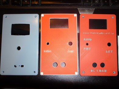
For housing he project I chose a basic grey project box and after "Hacking" the lid and being completely disgusted with the result and decided to 3D printed one

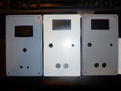
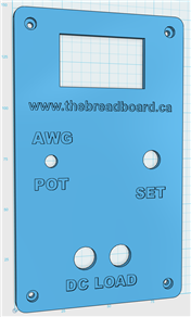
Here is my manual attempt next to my 3D printed versions, the middle version had no ribs on the back to support the walls of the main case and was also a tad thick so I modified it further to be more like the original and as you can see, asside from the text being too small or with a few small details that did not print correctly, it seemed to come out pretty good. I am still having difficulties with my printer but I can get some good prints out of it, btw, all of the holes came out exactly the correct sizes to no adjustments where needed. I will attached the design files for this so you can have a look and use for your own projects if you so desire.

imageimageimage

In order to get good measurements from the original (and I would suggest one of these to anyone doing 3D design), I used a Digital Engineering Caliper, this made getting the right and accurate measurements easy and quick

imageimage

You dont have to use an Electronic one, I just found it easier


below is an internal view of the build unit, as you can see, this is a one off so I simply used strip board and most components I had lying around. The heatsink if your wondering is from an old pc, it was the CPU Heatsink and has a fan already mounted on it. I was supprised how well it dissipated the heat from the FET. I guess it should when you consider older CPUs could easily require 150W of heat dissipation, I simply used existing holes to mount it to the plastic case and drilled and tapped holes to attach the FET and Current Sense Resistor (I did use a 100mOhm 1% Vishay Kelvin connection resistor for the current sense though image )

image

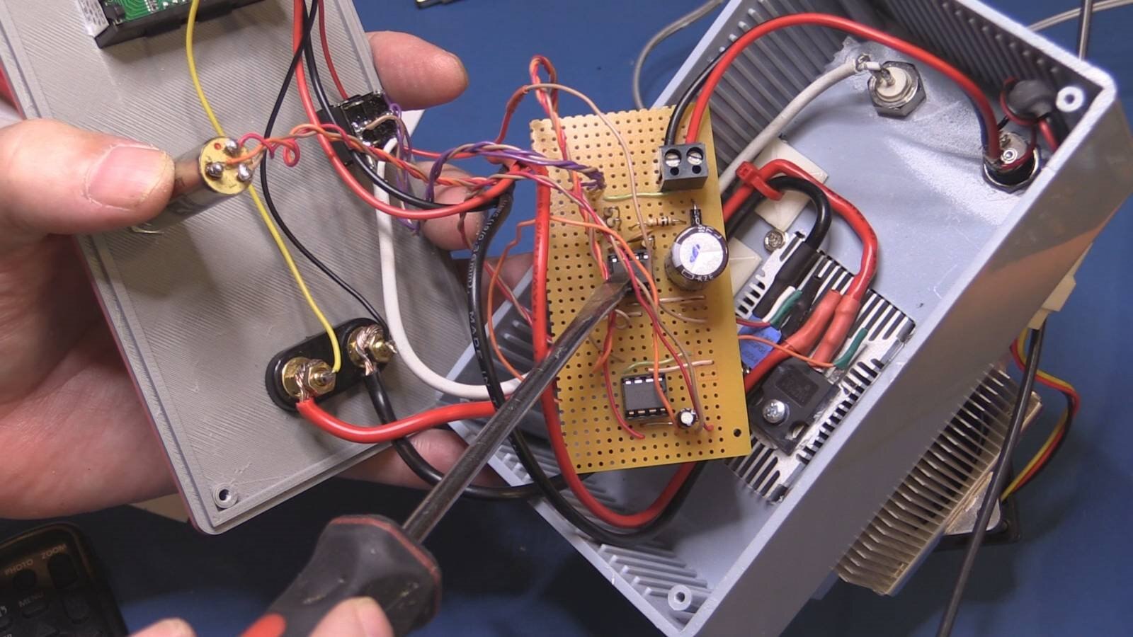
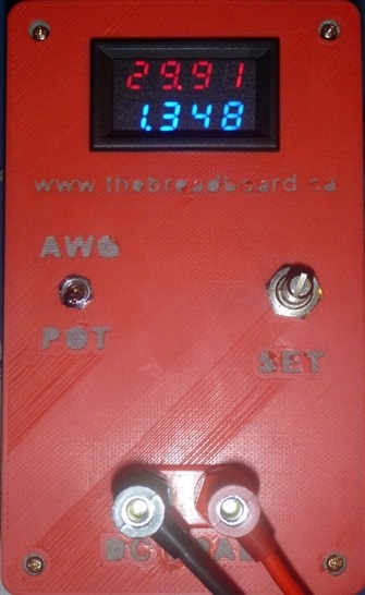
The connection top left is the input from an AWG or other 0 - 5V source, on the rear right is the 12V input jack, on the front panel you can clearly see the binding posts, the 10Turn pot (It is a bad fit as it is too long so I have others on order to replace it, they are not here though in time for this posting.The switch is in line with the pot and is used to select the POT output or the AWG input. I did not terminate the external input, I thought about putting a 50 Ohm resistor there, then decided it would be better to not have it inside and leave it to the user to add one external if needed, I also did not have another trim resistor of the correct value in a 10 turn type so it is also not yet installed, but as this does not need to be super accurate, it works just fine without it.


As i said, his DC load will handle plenty of power, I have already left it for several hours with 30V and 1.5Amps so 45 Watts, and it was barely above ambient and have also loaded with 60V at 1.5Amps with no ill effects so I have confidence it will perform for most of my desired uses and my next one will be far more capapable anyway.

Here is the video of the final build and testing

You don't have permission to edit metadata of this video.
Edit media
x
image
Upload Preview
image
,

here is a snap of the response time with a 2Khz sqare wave input, measured across a 1Ohm load so this shows a very good response with a 1Amp step in load

image


The display I have included provides 4 digits of remarkably accurate readings for voltage and current, I di hack it to allow the current sense to work in differential mode as initially the low side of the current sense resistor was tied to the oV of the panel supply, not sure whay but after removing this connection, the meter worked better in my solution

here is the schematic with the meter in place (Note the trimmer connections for the VREF are not correct in this drawing, refer to the one above for the corrections). this is just to show how the DPM is connected into the circuit, as the DPM current shunt is only 25mOhms, it has no noteable effect on the operation or the uniit under test.

image

I created a video of how the Hack was done etc, here it is for reference

You don't have permission to edit metadata of this video.
Edit media
x
image
Upload Preview
image

The only thing lacking right now is a fan control to slow it down when not running with a big load, this would be nice from a noise perspective but not essential

Attachments:
TopPanel 150x90.zip
90x150 top.zip
  • Sign in to reply

Top Comments

  • michaelkellett
    michaelkellett over 9 years ago in reply to Robert Peter Oakes +3
    I hope Peter won't mind if I add a little to his comments on power. Take a look at the IRFP064 data sheet (I'm using the Vishay one, RevC, 14 May 20111), , fig8, Maximum Safe Operating Area and you'll…
  • jc2048
    jc2048 over 9 years ago in reply to michaelkellett +2
    "So now we need to ask Peter if his circuit will be happy with 8 MOSFETs in parallel." Since you've dangled a worm in the stream, I'll bite, even though I'm just a minnow. [I don't have the kind of knowledge…
  • Robert Peter Oakes
    Robert Peter Oakes over 9 years ago +2
    To help with the whole paralleling of mosfets thing, here are 3 app notes that should ( ) explain all the things you need to know, the first two are full of math, the NXP is more related to what us mere…
  • Robert Peter Oakes
    Robert Peter Oakes over 9 years ago

    To help with the whole paralleling of mosfets thing, here are 3 app notes that should ( image ) explain all the things you need to know, the first two are full of math, the NXP is more related to what us mere mortals need to know

    http://www.irf.com/technical-info/appnotes/an-941.pdf

    http://www.infineon.com/dgdl/para.pdf?fileId=5546d462533600a401535744b4583f79

    https://cache.nxp.com/documents/application_note/AN11599.pdf

    • Cancel
    • Vote Up +2 Vote Down
    • Sign in to reply
    • More
    • Cancel
  • michaelkellett
    michaelkellett over 9 years ago in reply to jc2048

    I've had very bad experience attempting to parallel op amps - the voltage gain and offsets can vary significantly so you end up with a load of new sharing problems.


    There is an interesting Linear Technology article on the web about making a high current fast electronic load - the stray inductance is a  big potential problem.


    www.linear.com/docs/40550


    MK

    • Cancel
    • Vote Up 0 Vote Down
    • Sign in to reply
    • More
    • Cancel
  • jc2048
    jc2048 over 9 years ago in reply to michaelkellett

    Thanks Michael. As you say, compromises. Though in this case, without a tight spec, it's more design ideas or, perhaps, the voice of experience pointing us in a sensible direction.


    So the source resistors are similar to what you'd have to do paralleling up bipolar transistors, though for a different reason (in the bipolar case, to avoid thermal runaway, in this case to even-up small differences in the gate thresholds). Separate gate resistors mean that each MOSFET sees just its own gate capacitance and not the combination of all eight. And more drive from the op-amp because the existing part can only manage 10mA or so and we now need eight times the drive just to maintain the performance Peter had.


    It's interesting that once you've done all that, there's almost a case for simply replicating the control circuit eight times (especially since the op-amps are available in a quad version).


    Next step for me with the simulator, I think, is to look at driving the MOSFETs harder and faster to improve the dynamic performance. Whilst Peter's circuit is good for many applications, with modern switching regulators operating at ever higher frequencies, sometimes up to 1 or 2 MHz, we'd be in a situation where the regulator would be testing the test equipment rather than the other way round. (I can see that for a real-world test you'd just switch load resistors into circuit rather than attempt to get a control loop working fast enough, but it's an interesting design problem for me to have a go at.)

    • Cancel
    • Vote Up 0 Vote Down
    • Sign in to reply
    • More
    • Cancel
  • michaelkellett
    michaelkellett over 9 years ago in reply to jc2048

    Hello John,


    I'd match the MOSFETS if possible (but if you are only building one system you can't.) I'd replace the TLC072 with an op amp with more output drive capability (needs > 50mA to get reasonable slew rate into 100nF of gate load) and use a 100R gate resistor with each MOSFET. To share current you need an additional source resistor for each MOSFET, and ideally to drop 1V across each at full current (which is an additional 20W of loss but trivial in the context of out target 400W). You would need to use 0.4R resistors rated for at least 2.5W each - in fact you might do better to go up a bit on the resistors to 1R, 10W, at full power you would be putting 6.25W into each resistor (50W in total) but would get much better power sharing. The only problem is that the drop across the resistors at full current (2.5V) limits the lowest input voltage for full current.


    As ever - it's all compromises.


    MK

    • Cancel
    • Vote Up +1 Vote Down
    • Sign in to reply
    • More
    • Cancel
  • jc2048
    jc2048 over 9 years ago in reply to michaelkellett

    "So now we need to ask Peter if his circuit will be happy with 8 MOSFETs in parallel."


    Since you've dangled a worm in the stream, I'll bite, even though I'm just a minnow. [I don't have the kind of knowledge of these sort of areas of power electronics that you and Peter evidently do, but I'd like to learn a bit more.]


    Do you mean literally putting eight MOSFETs in parallel and then treating the combination as though it were one component, or do you mean replicating the MOSFET, sense resistor and amplifier eight times and putting those blocks in parallel?


    In the latter case, I'd expect it to work much as Peter's existing circuit, with the dynamic performance being much the same. It's a simple approach, but adds significantly to the component count.


    In the former I'd firstly worry about the spread on the Vgs thresholds (the Vishay datasheet gives a min of 2V and a max of 4V). Wouldn't there be the real danger of one or two of the devices hogging much of the current?


    But let's say that you matched the thresholds, so that the devices did share fairly evenly, you'd then have a device that would require eight times the charge into the (combined) gate over a single device [crudely, the input, instead of looking like 4nF-12nF of capacitance, would look more like 30nF-90nF) and the compensation capacitor would have to increase in order to give the same damping as the original because of the way everything has slowed down. The rise and fall times would increase (roughly by eight times) and hit the dynamic performance considerably. I don't think the circuit would be unhappy [it looks like the op-amp would manage], but the designer might be, depending on what they were trying to achieve. Things might be speeded up somewhat by allowing the op-amp to drive a bit more current into the gate and by reducing the compensation to be closer to the critically-damped case, but I suspect Peter chose the over-damped response because it gives a good margin against oscillation/ringing (which is an obvious worry if you are putting something out for people to build in an ad-hoc kind of way). On a simulation, if I reduce the compensation capacitor to the point that it's critically-damped (one overshoot), the edges start to get quite messy - Peter's response looks much cleaner because the R-C characteristic swamps everything else.


    How would you approach this, Michael, if you wanted to keep the original dynamic performance but spread the heat with eight MOSFETs?


    As a postscript, this taught me an excellent lesson when I tried simulating it. Unless you go in and start changing parameters on individual devices, the simulator gives you eight identical devices which, of course, share perfectly. So I now have another example of how easily you can go wrong if you just blindly accept what a quick, slapped-together simulation shows you.

    • Cancel
    • Vote Up +2 Vote Down
    • Sign in to reply
    • More
    • Cancel
<>
element14 Community

element14 is the first online community specifically for engineers. Connect with your peers and get expert answers to your questions.

  • Members
  • Learn
  • Technologies
  • Challenges & Projects
  • Products
  • Store
  • About Us
  • Feedback & Support
  • FAQs
  • Terms of Use
  • Privacy Policy
  • Legal and Copyright Notices
  • Sitemap
  • Cookies

An Avnet Company © 2026 Premier Farnell Limited. All Rights Reserved.

Premier Farnell Ltd, registered in England and Wales (no 00876412), registered office: Farnell House, Forge Lane, Leeds LS12 2NE.

ICP 备案号 10220084.

Follow element14

  • X
  • Facebook
  • linkedin
  • YouTube