element14 Community
element14 Community
    Register Log In
  • Site
  • Search
  • Log In Register
  • About Us
  • Community Hub
    Community Hub
    • What's New on element14
    • Feedback and Support
    • Benefits of Membership
    • Personal Blogs
    • Members Area
    • Achievement Levels
  • Learn
    Learn
    • Ask an Expert
    • eBooks
    • element14 presents
    • Learning Center
    • Tech Spotlight
    • STEM Academy
    • Webinars, Training and Events
    • Learning Groups
  • Technologies
    Technologies
    • 3D Printing
    • FPGA
    • Industrial Automation
    • Internet of Things
    • Power & Energy
    • Sensors
    • Technology Groups
  • Challenges & Projects
    Challenges & Projects
    • Design Challenges
    • element14 presents Projects
    • Project14
    • Arduino Projects
    • Raspberry Pi Projects
    • Project Groups
  • Products
    Products
    • Arduino
    • Avnet Boards Community
    • Dev Tools
    • Manufacturers
    • Multicomp Pro
    • Product Groups
    • Raspberry Pi
    • RoadTests & Reviews
  • Store
    Store
    • Visit Your Store
    • Choose another store...
      • Europe
      •  Austria (German)
      •  Belgium (Dutch, French)
      •  Bulgaria (Bulgarian)
      •  Czech Republic (Czech)
      •  Denmark (Danish)
      •  Estonia (Estonian)
      •  Finland (Finnish)
      •  France (French)
      •  Germany (German)
      •  Hungary (Hungarian)
      •  Ireland
      •  Israel
      •  Italy (Italian)
      •  Latvia (Latvian)
      •  
      •  Lithuania (Lithuanian)
      •  Netherlands (Dutch)
      •  Norway (Norwegian)
      •  Poland (Polish)
      •  Portugal (Portuguese)
      •  Romania (Romanian)
      •  Russia (Russian)
      •  Slovakia (Slovak)
      •  Slovenia (Slovenian)
      •  Spain (Spanish)
      •  Sweden (Swedish)
      •  Switzerland(German, French)
      •  Turkey (Turkish)
      •  United Kingdom
      • Asia Pacific
      •  Australia
      •  China
      •  Hong Kong
      •  India
      •  Korea (Korean)
      •  Malaysia
      •  New Zealand
      •  Philippines
      •  Singapore
      •  Taiwan
      •  Thailand (Thai)
      • Americas
      •  Brazil (Portuguese)
      •  Canada
      •  Mexico (Spanish)
      •  United States
      Can't find the country/region you're looking for? Visit our export site or find a local distributor.
  • Translate
  • Profile
  • Settings
Test & Tools
  • Technologies
  • More
Test & Tools
Blog Review and test a 0 - 1mA constant current source
  • Blog
  • Forum
  • Documents
  • Files
  • Members
  • Mentions
  • Sub-Groups
  • Tags
  • More
  • Cancel
  • New
Join Test & Tools to participate - click to join for free!
  • Share
  • More
  • Cancel
Group Actions
  • Group RSS
  • More
  • Cancel
Engagement
  • Author Author: Jan Cumps
  • Date Created: 9 Mar 2024 11:05 AM Date Created
  • Views 5588 views
  • Likes 10 likes
  • Comments 19 comments
  • pico
  • labview
Related
Recommended

Review and test a 0 - 1mA constant current source

Jan Cumps
Jan Cumps
9 Mar 2024
Review and test a 0 - 1mA constant current source

 shabaz designed an OpAmp based constant current source. It can deliver up to 1 mA. The current is controlled by a voltage. It's intended to be used with a DAC board for the Raspberry Pico. A constant current is a useful lab instrument. It can be used for testing semiconductors, and in sorts of circuits where components are driven by a current.

image

Specification:

  • constant current between 0 and 1 mA
  • control voltage: 0 - 1 V
  • compliance: 3 V (4.5 V with a LM324)
  • power rails: - 1.5 V and + 3.3 V (+5 V with LM324

How does it work?

High level: the circuit is built around a differential amplifier design (UA1). See also the internals of an INA106 differential amplifier a bit further down this post, and try to find similarities to this circuit. 

image
image source: shabaz' schematic

I removed the two extra current drivers U1C and U1D for the time being, to make the likeness more striking. We 'll add them back later and tell how they impact the output current.

I also made reorganising changes, that don't alter the circuit: I 've drawn U1B pointing back, and moved a few resistors up-down, to make the next step in the analysis easier.

image
image source: shabaz' schematic, edited

The exact same circuit is discussed in The Art Of Electronics. They draw it a little different, with the feedback x1 gain buffer pointing back. My edits of the original circuit (above, with Microsoft Paint) were done to show the concept similarity.

image
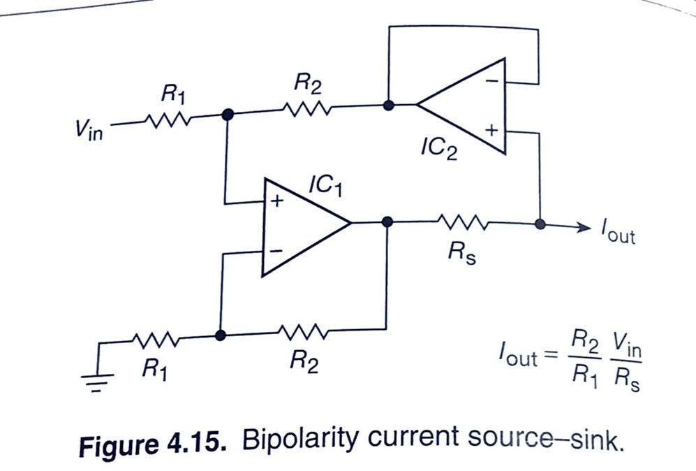
image source: my copy of The Art Of Electronics (TAOE), 2nd edition

In the drawing of shabaz, and in the TAOE schematic, you should now clearly see that it's identical to what's inside a differential amplifier:

image
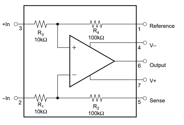
image source: TI (BB) INA106 differential amplifier data sheet, edited. I flipped the original drawing vertically, to show the same orientation as the circuits above

Note that if you 'd use Reference and Sense as +In and -In, and vice-versa: use +In and -In as Reference and Sense, it would be an almost perfect (better, because R1 -> R4 are factory-matched in the INA106 !) drop-in replacement for U1A.

So we can summaries that the circuit works like one, and measures the voltage over the sense resistor (R5 in shabas' design). It measures the voltage over the sense resister (that also means: the current through it), and tries to keep the design stable. If you add voltage to the reference input (U1A in +) , it will increase the voltage over R5 to get back into balance. Thus, more current will flow through R5, and we increase the constant current output. The differential amp keeps this in balance.

The buffer at the output (U1B) takes care that there's no current error. It feeds back the output voltage without loading that output.

In TAOE, we can see that the formula for output current is:

image

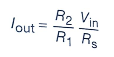
If we plug shabaz' values in that formula:

image

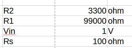
the outcome = (3300 ohm / 99000 ohm) x (1 volt / 100 ohm) = 0.333 mA.

But the specs say it's 1 mA. Why the difference? That's where the two current drivers U1C and U1D and their output resistor come into place. They have a gain of 1, take care that the same current is sent additionally to the exit node. 3 x 0.333 mA = 1 mA.

Another way of seeing it, is that the combination of Rs (R5, R6, R7) is an "active 33 ohm resistor". If we plug that value in the formula: (3300 / 99000) x (1 / 33) = 1 mA.

Characterising the circuit

I've created a LabVIEW flow to characterise the behaviour. As RLOAD, I used a DMM in DC current mode.

Here's what the flow does:

  • set up V- and V+, as channel 1 and 2 of a Rigol DP832A PSU
  • set up Vcontrol as channel 3 of that PSU
  • enable the PSU outputs
  • set DMM6500 to current measure mode, range 1 mA (range, and measurement noise handling parameters, can be changed)
  • step through Vcontrol from 0 V to 1V in definable steps.
  • allow the Vcontrol to optionally settle between steps (settle time can be changed)
  • show the results on screen, and log to a spreadsheet

image

image
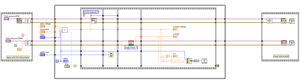
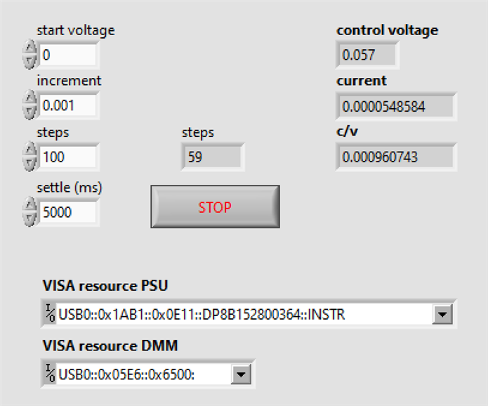
image sources: my LabVIEW design

Here is the output current, when I take 100 little 1mV steps from 0 to 1V

image
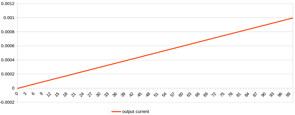
image source: the spreadsheet samples on a graph. X = steps (1 mV increments), Y = output current.

Based on how long I let the PSU settle each step before measuring, and the precision options that I set on the DMM, sampling a 100 step sweep can run from 50 seconds to hours. If I'd custimise / optimise the Rigol blocks, I'm sure I'd be able to get this below 10 seconds.

For reference, I attached a file with:

  • 100 samples, sweep Vcontrol between 0 and 100 mV
  • settle the PSU after each step for 5 seconds
  • DMM in 1mA rande
  • integrate each measurement over 10 mains power cycles
  • average 10 measurements over each sample
  • ignore column B, control voltage. It comes from the PSU but is not reliable. For the set voltage, take the steps value in column A (in mV).

characterize_100steps_5sec_10nlpc_10avg_autozero.xlsx

Thank you for reading.

  • Sign in to reply

Top Comments

  • michaelkellett
    michaelkellett over 1 year ago in reply to shabaz +2
    You could try OPA4192 (available in SOIC, same pinout as MCP6024) OPA4192 approx £6 each offset 25uV, max output current approx 20mA (1V drop), max supply (working) +/-18V MCP6024 approx £2 each…
  • jc2048
    jc2048 over 1 year ago +1
    Good blog! Few random thoughts and ideas 1. Output compliance with an old LM324 won't be 4.5V on a 5V supply (the top driver is a darlington pair, so there's at least 2 Vbe drops down from the rail…
  • jc2048
    jc2048 over 1 year ago in reply to Jan Cumps +1
    This is what Tina-TI shows for sweeping the compliance voltage slowly over a second. That's using Microchip's model for the opamp as it comes. It won't match reality for several reasons, but it's…
Parents
  • Jan Cumps
    Jan Cumps over 1 year ago

    LTSpice simulation

    image

    3157.constant_current_source.zip

    The current lands slightly above the 1mA, because I set Rs as 33 ohm. It should be 100 ohm / 3 = 33.3 ohm. In that case the line lands on 1 mA for Vctrl = 1 V:

    image

    • Cancel
    • Vote Up 0 Vote Down
    • Sign in to reply
    • More
    • Cancel
  • jc2048
    jc2048 over 1 year ago in reply to Jan Cumps

    This is what Tina-TI shows for sweeping the compliance voltage slowly over a second.

    image

    image

    That's using Microchip's model for the opamp as it comes. It won't match reality for several reasons, but it's indicative of the kind of thing you might see and how it might vary, though treat it as more of a worst case rather than a precise prediction.

    As far as I know, chip models are by characterisation, they're not physically modelled (too slow and gives too much away about the internal design), so some care is needed with simulation - some things may not be modelled (like how the part functions if you take pins outside the supply voltage range, etc, and they'll have chosen typical values for the things with a spread (like the open-loop gain, offsets, etc). With an analogue part like this, the manufacturer needs to put something in for the offset voltage (it's cheating to leave it at zero and pretend it's perfect, even though that may be the average they see). I don't know how they do that - maybe for a normal distribution they take the 1-sigma point, or something like that, but whatever they do it will skew things a bit.

    If anyone wants to try this in Tina-TI, don't use the standard analysis settings, chose the ones for low voltages and currents.

    I'd be interested in whether Jan's board matches that in any way whatsoever. The way it's varying over the compliance range looks a little too neat to me (like they've just gone for a straight-line approximation to a much more complex curve when they measured it).

    It settles ok (with just a fixed voltage at the output). This is for a 10kHz 1V squarewave (10ns edge) at the input. This is the top of the output current with the output voltage stepped in 1V increments. (Red is 0V, blue is 3V.)

    image

    image

    And this the bottom.

    Of course, there's another source of inaccuracy, that this simulation doesn't even touch, and that's the resistance tolerances. For a one-off, matching values and ratios between values is quite possible, with a bit of effort.

    • Cancel
    • Vote Up +1 Vote Down
    • Sign in to reply
    • More
    • Cancel
  • Jan Cumps
    Jan Cumps over 1 year ago in reply to jc2048

    > matching values and ratios between values is quite possible, with a bit of effort.

    I didn't use precision resistors (E24, 5%) nor checked if the ones I used match. They are from the same cut tape - so I expect from the same batch - though.

    • Cancel
    • Vote Up 0 Vote Down
    • Sign in to reply
    • More
    • Cancel
  • shabaz
    shabaz over 1 year ago in reply to jc2048

    Hi Jon,

    Thanks for simulating this! 

    • Cancel
    • Vote Up 0 Vote Down
    • Sign in to reply
    • More
    • Cancel
  • Jan Cumps
    Jan Cumps over 1 year ago in reply to jc2048

    The theoretical OpAmp in LTSpice shows the same compliance behaviour.

    Single sweep of V4 between 0 and 3 V with constant Vctrl = 1V.

    image

    • Cancel
    • Vote Up 0 Vote Down
    • Sign in to reply
    • More
    • Cancel
  • Jan Cumps
    Jan Cumps over 1 year ago in reply to jc2048

    The real board tells a different story. I lifted the voltage under the load with 0, 1, 2 and 3 V, with Vctrl = 700 mV.

    image
    imageimageimage

    The offset supply was wired the same as the VG1 in the TI-TINA schematic.

    Current went slightly up when I increased the bias.

    • 0 V: 693 µA
    • 1 V: 696 µA
    • 2 V: 701 µA
    • 3 V: 702 µA 

    The sense resistor in the DMM for the 1 mA range is 135 Ohm. +- 90 mV over the meter at the set current.

    Then a steep drop when I moved closer to the rail, over 3.1 V, as expected. Too steep to be able to control it with my rudimentary power supply, so no reliable measurements.. 

    • Cancel
    • Vote Up 0 Vote Down
    • Sign in to reply
    • More
    • Cancel
  • jc2048
    jc2048 over 1 year ago in reply to Jan Cumps

    My simulation isn't quite as useful as it looks.

    There's nothing to stop us measuring the offset in the model by experimenting in exactly the same way as we might with a real component, so here goes.

    image

    Here, I'm sweeping the voltage VG1 from 0V to 3V and measuring the offset at the input pins as the opamp follows it.

    That gives me this.

    image

    This is the measured distribution from the datasheet, so I was wrong and the approx 300uV value in the model is actually fairly close to being a worst-case one.

    image


    However, for the variation over the common-mode voltage range, the model is definitely a very simple straight-line approximation. In the datasheet they show the results of measuring actual devices, and it looks like this

    image


    That's probably not too surprising with a CMOS rail-to-rail input where there has to be merging of two input circuits with slightly different characteristics, but it means that my nice, neat, evenly spaced waveforms are merely fiction.

    Beware simulation models!

    • Cancel
    • Vote Up 0 Vote Down
    • Sign in to reply
    • More
    • Cancel
Comment
  • jc2048
    jc2048 over 1 year ago in reply to Jan Cumps

    My simulation isn't quite as useful as it looks.

    There's nothing to stop us measuring the offset in the model by experimenting in exactly the same way as we might with a real component, so here goes.

    image

    Here, I'm sweeping the voltage VG1 from 0V to 3V and measuring the offset at the input pins as the opamp follows it.

    That gives me this.

    image

    This is the measured distribution from the datasheet, so I was wrong and the approx 300uV value in the model is actually fairly close to being a worst-case one.

    image


    However, for the variation over the common-mode voltage range, the model is definitely a very simple straight-line approximation. In the datasheet they show the results of measuring actual devices, and it looks like this

    image


    That's probably not too surprising with a CMOS rail-to-rail input where there has to be merging of two input circuits with slightly different characteristics, but it means that my nice, neat, evenly spaced waveforms are merely fiction.

    Beware simulation models!

    • Cancel
    • Vote Up 0 Vote Down
    • Sign in to reply
    • More
    • Cancel
Children
No Data
element14 Community

element14 is the first online community specifically for engineers. Connect with your peers and get expert answers to your questions.

  • Members
  • Learn
  • Technologies
  • Challenges & Projects
  • Products
  • Store
  • About Us
  • Feedback & Support
  • FAQs
  • Terms of Use
  • Privacy Policy
  • Legal and Copyright Notices
  • Sitemap
  • Cookies

An Avnet Company © 2025 Premier Farnell Limited. All Rights Reserved.

Premier Farnell Ltd, registered in England and Wales (no 00876412), registered office: Farnell House, Forge Lane, Leeds LS12 2NE.

ICP 备案号 10220084.

Follow element14

  • X
  • Facebook
  • linkedin
  • YouTube