element14 Community
element14 Community
    Register Log In
  • Site
  • Search
  • Log In Register
  • Community Hub
    Community Hub
    • What's New on element14
    • Feedback and Support
    • Benefits of Membership
    • Personal Blogs
    • Members Area
    • Achievement Levels
  • Learn
    Learn
    • Ask an Expert
    • eBooks
    • element14 presents
    • Learning Center
    • Tech Spotlight
    • STEM Academy
    • Webinars, Training and Events
    • Learning Groups
  • Technologies
    Technologies
    • 3D Printing
    • FPGA
    • Industrial Automation
    • Internet of Things
    • Power & Energy
    • Sensors
    • Technology Groups
  • Challenges & Projects
    Challenges & Projects
    • Design Challenges
    • element14 presents Projects
    • Project14
    • Arduino Projects
    • Raspberry Pi Projects
    • Project Groups
  • Products
    Products
    • Arduino
    • Avnet & Tria Boards Community
    • Dev Tools
    • Manufacturers
    • Multicomp Pro
    • Product Groups
    • Raspberry Pi
    • RoadTests & Reviews
  • About Us
    About the element14 Community
  • Store
    Store
    • Visit Your Store
    • Choose another store...
      • Europe
      •  Austria (German)
      •  Belgium (Dutch, French)
      •  Bulgaria (Bulgarian)
      •  Czech Republic (Czech)
      •  Denmark (Danish)
      •  Estonia (Estonian)
      •  Finland (Finnish)
      •  France (French)
      •  Germany (German)
      •  Hungary (Hungarian)
      •  Ireland
      •  Israel
      •  Italy (Italian)
      •  Latvia (Latvian)
      •  
      •  Lithuania (Lithuanian)
      •  Netherlands (Dutch)
      •  Norway (Norwegian)
      •  Poland (Polish)
      •  Portugal (Portuguese)
      •  Romania (Romanian)
      •  Russia (Russian)
      •  Slovakia (Slovak)
      •  Slovenia (Slovenian)
      •  Spain (Spanish)
      •  Sweden (Swedish)
      •  Switzerland(German, French)
      •  Turkey (Turkish)
      •  United Kingdom
      • Asia Pacific
      •  Australia
      •  China
      •  Hong Kong
      •  India
      •  Japan
      •  Korea (Korean)
      •  Malaysia
      •  New Zealand
      •  Philippines
      •  Singapore
      •  Taiwan
      •  Thailand (Thai)
      •  Vietnam
      • Americas
      •  Brazil (Portuguese)
      •  Canada
      •  Mexico (Spanish)
      •  United States
      Can't find the country/region you're looking for? Visit our export site or find a local distributor.
  • Translate
  • Profile
  • Settings
Test & Tools
  • Technologies
  • More
Test & Tools
Documents Programmable Electronic Load - Power Stage
  • Blog
  • Forum
  • Documents
  • Files
  • Members
  • Mentions
  • Sub-Groups
  • Tags
  • More
  • Cancel
  • New
Join Test & Tools to participate - click to join for free!
Actions
  • Share
  • More
  • Cancel
Engagement
  • Author Author: Jan Cumps
  • Date Created: 20 Dec 2017 7:20 PM Date Created
  • Last Updated Last Updated: 11 Oct 2020 8:07 AM
  • Views 6948 views
  • Likes 7 likes
  • Comments 68 comments
Related
Recommended

Programmable Electronic Load - Power Stage

This blog documents focuses on the power stage of the electronic load that Robert Peter Oakes, jc2048 and Jan Cumps are designing.


image

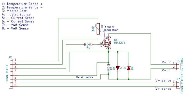
In this post we're laying out a PCB for the power stage - as much as possible with surface mount components. The FET is close to the one Robert Peter Oakes uses in the original design.


The BOM


ComponentHeader 2Header 3Header 4
P18 pin header, 2.54mm
P2 abinding post, redhirschmann 931714101hirschmann 931714101 -  SOCKET, 4MM, BLACK, PK5 , MLS
P2 bbinding post, blackhirschmann 931714100hirschmann 931714100 -  SOCKET, 4MM, BLACK, PK5 , MLS
P3 abinding post, blacktenma 2301tenma 2301 - Binding Post, 36 A, 500 V, Nickel Plated Contacts, Panel Mount, Black
P3 bbinding post, redtenma 2302tenma 2302 - Binding Post, 36 A, 500 V, Nickel Plated Contacts, Panel Mount, Red
TH1NTC Thermistor, 10KVishay NTCS0805E3103JLTVishay NTCS0805E3103JLT -  THERMISTOR, 10K, 5%, SMD, NTC
Q1N-Channel MosfetInfineon IRF3205SPBFInfineon IRF3205SPBF -  MOSFET Transistor, N Channel, 110 A, 55 V, 8 mohm, 10 V, 4 V
D1, D2DiodeDIODES SBR2A40P1-7DIODES SBR2A40P1-7 -  Standard Recovery Diode, PowerdiRegistered, 40 V, 2 A, Single, 500 mV, 50 A
R1100R1206 any brand
R20R05Vishay WSHP2818R0500FEBVishay WSHP2818R0500FEB -  SMD Current Sense Resistor, 0.05 ohm, 10 W, 2818 [7146 Metric], ± 1%, WSHP2818 Series
Cooler HeatsinkStartech.com FAN370PRO - Socket 7/370 CPU Cooler Heatsink and Fan


NTC


For a detailed description on the temperature protection mechanism, check Programmable Electronic Load - Temperature Protection.


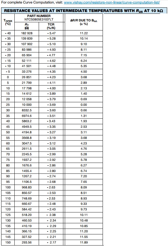
The voltage sent to the ADC is very dependent on the NTC. I've selected a Vishay NTCS0805E3103JLTVishay NTCS0805E3103JLT -  THERMISTOR, 10K, 5%, SMD, NTC.

I'll program the key values. The behaviour is non-linear and it's easier to make a lookup table if the firmware has to be able to deal with different components.

This will require access to flash to permanently store tha values, and a SCPI function to alter the table if another component is used.

For the first version I'm going to be selfish and just program for the device that I've ordered.

image


PCB


Exposed copper


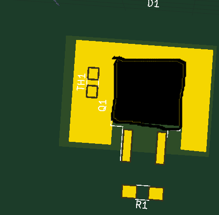
For good thermal relief, and to get the NTC as good termally coupled to the FET as possible,

I placed a copper pour (here on the front, I'll do the same on the back and stitch them for thermal transport with vias)

Then i drew a pour on the front mask. The area of pour will expose copper. That means that the NTC has physical contact with the copper that the FET is soldered on.

In the fine-tuning I will place that NTC closer to the FET so that I can put a tad of heat paste in between. Or I could put a tad of paste between the NTC and exposed copper ...

image


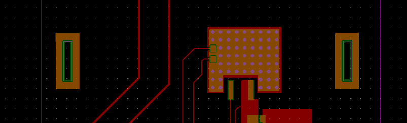
Attention when placing the binding posts. For the power input, RED is 1 and BLACK is 2.

For the sense input, BLACK is 1 and RED is 2.

This is the result of me labeling pin 7 and 8 of the connectors between the driver board and FET board wrong, on both boards image.

The documentation and KiCAD zips are now updated with corrected schematics.


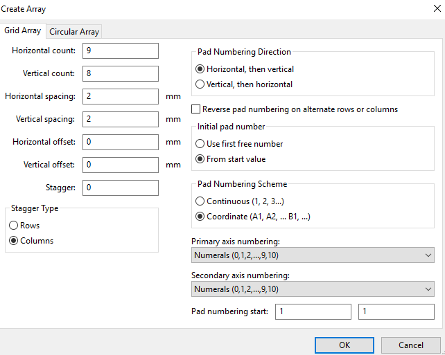
I used these 2 Contextual Electronics videos to refresh how to expose copper layers and place VIA arrays:
You don't have permission to edit metadata of this video.
Edit media
x
image
Upload Preview
image
You don't have permission to edit metadata of this video.
Edit media
x
image
Upload Preview
image


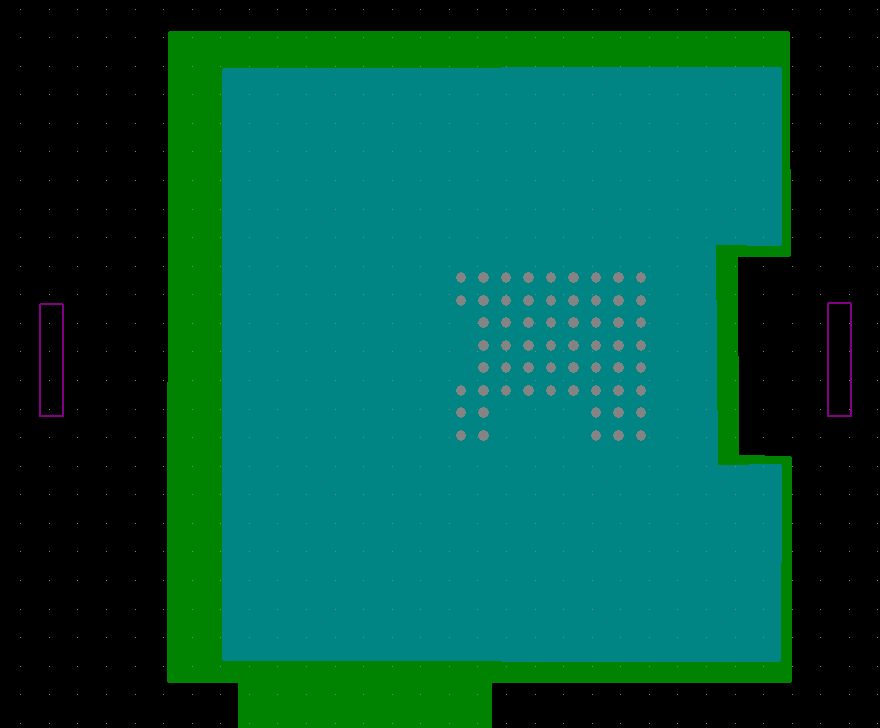
Here's the top side of the completed design. I've drawn the FET in green to give perspective.

image

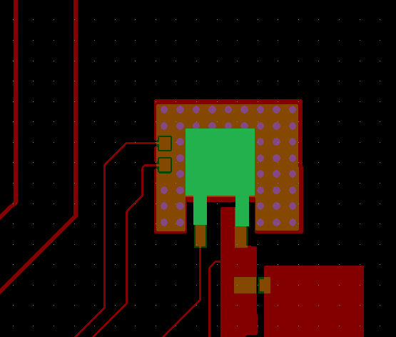
In red you see the copper layer, orange is where the solder mask is removed and copper exposed.

Pink are the drill holes. They are 0.9652 mm, in an array of 9 * 8, spaced 2 mm apart.

image


On the bottom, the copper pad (green) has the size of my heat sink + some. The removed mask (blue) has the exact size of the sink's bottom profile.

The pink lines are the mounting slots for the heat sink (see below).

image


Slots


My heat sink has brackets for mounting. I've cut out slots to allow the brackets to through the PCB and fix them on the top side.


image


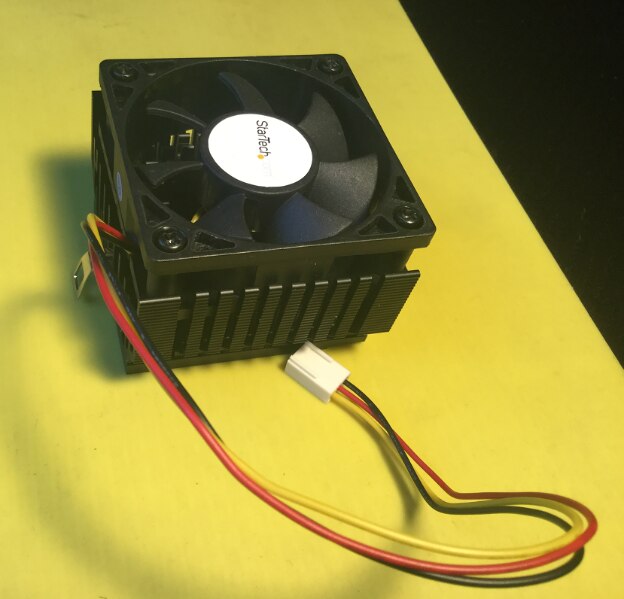
I've put some exposed non-connected copper pour around the slots for strength.

The slot is drawn on the Edge.Cuts layer. I hope that the PCB fab interprets that as slots to be milled out ...

image


I've attached the KiCAD project, component libs and Gerbers in a single zip. Also the VIA lib that's used here as a separate file (because I share that one across projects).

Attachments:
vias.pretty.zip
eload_offboard_20171227.zip
  • mosfet
  • metrology
  • ntc
  • msp432
  • scpi
  • laboratory
  • instrument
  • Share
  • History
  • More
  • Cancel
  • Sign in to reply

Top Comments

  • shabaz
    shabaz over 8 years ago in reply to Jan Cumps +4
    That looks great! Looks like Kicad is quite usable, you're getting good results. I've yet to try it.
  • Jan Cumps
    Jan Cumps over 8 years ago +3
    PCBs have arrived from Seeed. The heatsink fits perfect on the pad. The slots for the mounting bracket turned out OK.
  • Robert Peter Oakes
    Robert Peter Oakes over 8 years ago in reply to Jan Cumps +3
    They look great
  • Jan Cumps
    Jan Cumps over 8 years ago in reply to Jan Cumps

    image


    Most components placed, except the header and the power jacks.


    The NTC was a bit tricky because there's no solder mask (for better thermal transfer)

    • Cancel
    • Vote Up +3 Vote Down
    • Sign in to reply
    • More
    • Cancel
  • Jan Cumps
    Jan Cumps over 8 years ago

    The components arrived. Yay!

    image

    • Cancel
    • Vote Up +2 Vote Down
    • Sign in to reply
    • More
    • Cancel
  • Jan Cumps
    Jan Cumps over 8 years ago in reply to shabaz

    shabaz  wrote:


    That looks great! Looks like Kicad is quite usable, you're getting good results. I've yet to try it.

    Yes, everything that I wanted to do with my PCBs was possible. Not always obvious how to do something, but there's good documentation and how-to's available.

    What it doesn't offer in general is efficiency-boosting functions that you find in the up-market packages, asides from Push&Shove.

    • Cancel
    • Vote Up +3 Vote Down
    • Sign in to reply
    • More
    • Cancel
  • Robert Peter Oakes
    Robert Peter Oakes over 8 years ago in reply to Jan Cumps

    They look great

    • Cancel
    • Vote Up +3 Vote Down
    • Sign in to reply
    • More
    • Cancel
  • shabaz
    shabaz over 8 years ago in reply to Jan Cumps

    That looks great! Looks like Kicad is quite usable, you're getting good results. I've yet to try it.

    • Cancel
    • Vote Up +4 Vote Down
    • Sign in to reply
    • More
    • Cancel
  • Jan Cumps
    Jan Cumps over 8 years ago

    PCBs have arrived from Seeed.


    imageimage


    The heatsink fits perfect on the pad. The slots for the mounting bracket turned out OK.

    image

    • Cancel
    • Vote Up +3 Vote Down
    • Sign in to reply
    • More
    • Cancel
  • Robert Peter Oakes
    Robert Peter Oakes over 8 years ago in reply to Jan Cumps

    Phew, you had me worried for a moment

    • Cancel
    • Vote Up 0 Vote Down
    • Sign in to reply
    • More
    • Cancel
  • Jan Cumps
    Jan Cumps over 8 years ago in reply to Robert Peter Oakes

    Robert Peter Oakes  wrote:


    72 euros for 3?, is seed studio starting to gt expensive ? or is that a typo, i thought with little boards it was nearer 10 Euros... of course I may be mistaken

    That's the OSH Park price for 3 including shipping. Seeed is approx 36 € including shipping for the 10.

    • Cancel
    • Vote Up 0 Vote Down
    • Sign in to reply
    • More
    • Cancel
  • Robert Peter Oakes
    Robert Peter Oakes over 8 years ago in reply to Jan Cumps

    72 euros for 3?, is seed studio starting to gt expensive ? or is that a typo, i thought with little boards it was nearer 10 Euros... of course I may be mistaken

    • Cancel
    • Vote Up +1 Vote Down
    • Sign in to reply
    • More
    • Cancel
  • Robert Peter Oakes
    Robert Peter Oakes over 8 years ago in reply to michaelkellett

    I would suggest thickening up the wires coming from the high power areas to the o.1" connector, even though there minimal current, it may mitigate frying the traces if you accidentally short two pins together briefly image, the rest of the copper is not being used for much anyway outside of the heat pad.

    • Cancel
    • Vote Up +1 Vote Down
    • Sign in to reply
    • More
    • Cancel
<>
element14 Community

element14 is the first online community specifically for engineers. Connect with your peers and get expert answers to your questions.

  • Members
  • Learn
  • Technologies
  • Challenges & Projects
  • Products
  • Store
  • About Us
  • Feedback & Support
  • FAQs
  • Terms of Use
  • Privacy Policy
  • Legal and Copyright Notices
  • Sitemap
  • Cookies

An Avnet Company © 2026 Premier Farnell Limited. All Rights Reserved.

Premier Farnell Ltd, registered in England and Wales (no 00876412), registered office: Farnell House, Forge Lane, Leeds LS12 2NE.

ICP 备案号 10220084.

Follow element14

  • X
  • Facebook
  • linkedin
  • YouTube