Table of Contents
- The maker's nightmare.
- Switched Mode Power Supplies SMPS and Linear Power Supplies
- Comercial SMPS Flyback Converters
- Regulation in flyback converters
- Choosing the victim. Creatively torturing an SMPS transformer.
- Experiment 1: Working as a linear power transformer
- Experiment 2: Pulse response
- Experiment 3: Pulse response, secondary rectifier diode and capacitor
- Experiment 4: Generating a 100 kHz PWM signal with a microcontroller.
- Experiment 5: Using an optocoupler to drive the MOSFET switch from the microcontroller
- Experiment 6: Using BJT transistors to drive the MOSFET from the microcontroller
- Experiment 7: Blindly and Erroneously Optimizing the MOSFET driver.
- Experiment 8: 1st Don't Try This. Flyback converter without primary snubber.
- Experiment 9: 2nd Don't Try This. Flyback converter with primary snubber.
- Experiment 9: Gluing it all together my first unregulated DC/DC flyback converter.
- Summary and conclusions
- Magic Lightbox Blog Series
The maker's nightmare.
Everyone knows that we makers love blinking LEDs, a good project is not finished if it does not have its elegant blinking LEDs. But in this project, we are going to do the opposite, we are going to try to build a circuit based on the topology of the flyback DC/DC converters that keeps an LED illuminated constantly, without any flickering. A maker's nightmare.
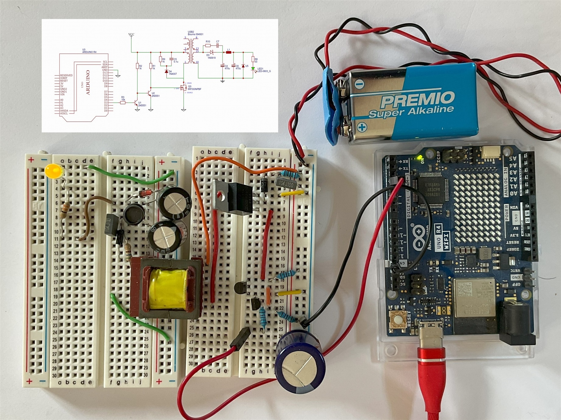
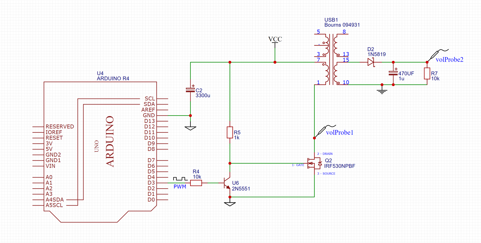
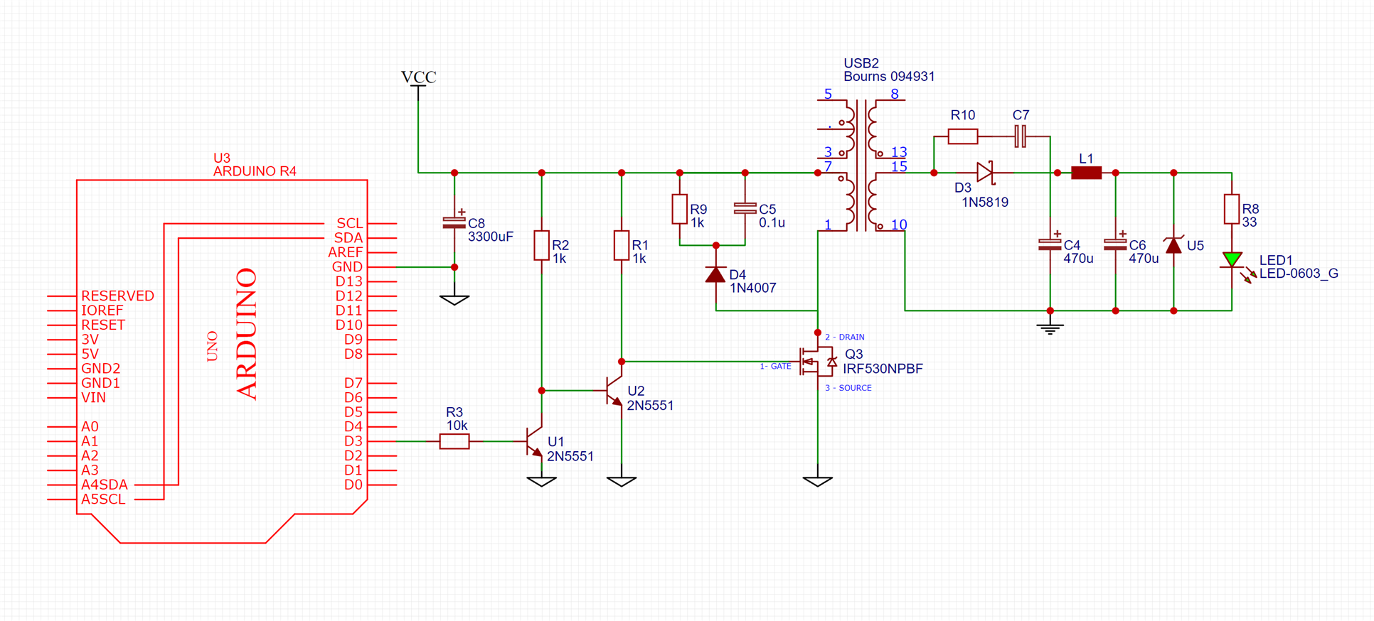
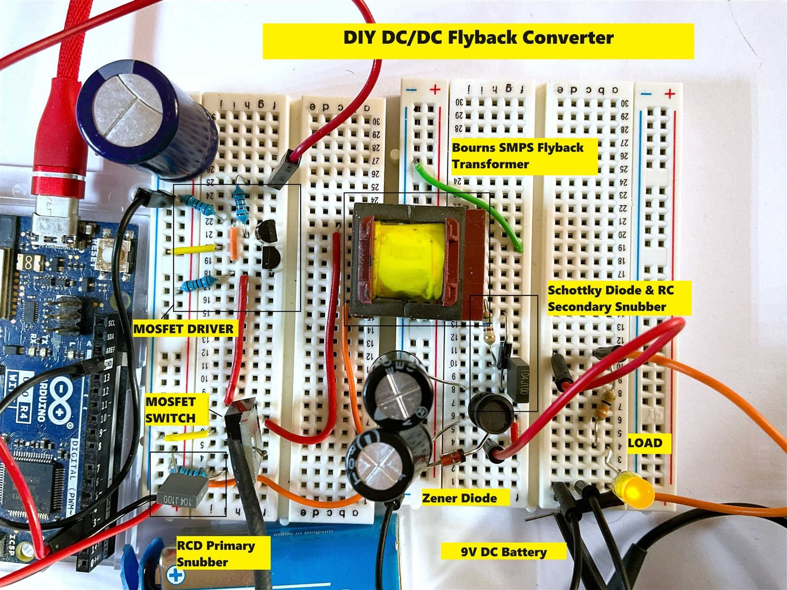
What are we going to build? We will craft a fancy unregulated flyback switched mode DC/DC converter circuit controlled by an Arduino UNO R4 microcontroller just to light up a humble LED with a 9V battery. Let's build the circuit you see in the image. We are going to build it experimentally without doing any calculations, just based on intuition and the measurements that we obtain as we design the different blocks of the circuit. My little son summed it up perfectly: it's a whole circuit just for one little light. Seems like our LED is getting the VIP treatment!
Switched Mode Power Supplies SMPS and Linear Power Supplies
First we will explore the world of power supplies with Switched Mode Power Supplies (SMPS) and Linear Power Supplies. Learn the distinctions and applications in this brief introduction.
A linear power supply is a type of electronic power supply that provides a constant output voltage by dissipating excess power in the form of heat. It typically consists of a transformer, rectifier, and a linear regulator. Linear power supplies are simpler and have a straightforward design. They also have a low level of output ripple but are less efficient compared to switched-mode power supplies, especially when the voltage difference between input and output is significant. The linear regulator dissipates excess energy as heat, which is drawback in terms of energy efficiency. Linear power supplies are commonly used in applications where simplicity, low cost, and low noise are prioritized over energy efficiency, such as in audio amplifiers, test and measurement equipment, and some small electronic devices.
A Switched-Mode Power Supply (SMPS) is another type of electronic power supply that uses switching devices, such as transistors, to control the power flow and efficiently regulate the output voltage. Unlike linear power supplies that dissipate excess energy as heat, SMPS adjusts the input power to provide the desired output voltage, resulting in higher efficiency.
A flyback converter is a type of switched-mode power supply (SMPS) that uses the energy storage and transfer capabilities of a gapped transformer to convert input voltage to the desired output voltage. It is known for its simplicity, compact design, and ability to provide galvanic isolation between the input and output. Some of the disadvantages of Flyback Converters are the voltage spikes due to the discontinuous energy transfer and the need for a feedback loop that adds complexity to the control circuitry.

In a typical flyback transformer, you’ll find a switch connected to the primary winding. The switch is usually in the form of a power transistor. When the switch is turned on, the magnetic field is gradually built-up on the core. A diode is placed on the secondary part of the transformer so that no current goes through during the energy build up stage. When the transistor is turned off, the current is cut off from the primary winding. As such, the voltage polarity changes to the opposite on the secondary winding and current is released on the circuit. Then, a capacitor after the secondary winding stores the electrical energy and smooths the ripples generated by the fast switching speed of the transistor.
Comercial SMPS Flyback Converters
Let's see what's inside two small mobile chargers. The following two images show us two generations of mobile chargers. The image on the left is of a mobile charger for an old Nokia 3110 and the charger on the right corresponds to a somewhat more modern LG brand mobile charger.
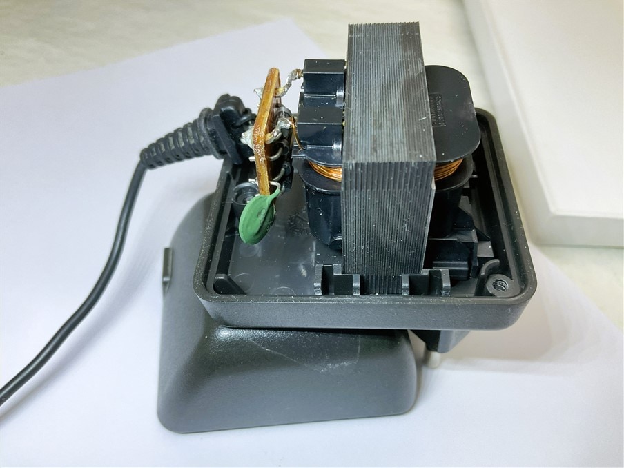
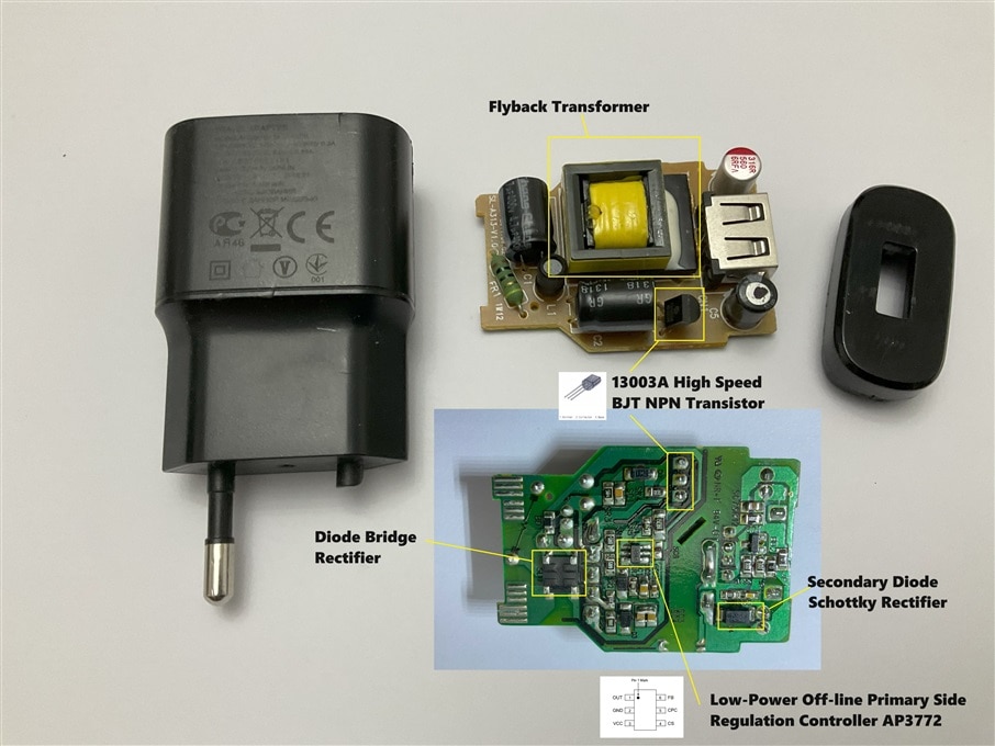
Unregulated Nokia Power Supply and Small LG Mobile Phone Charger Power Supply
The Nokia charger was a small unregulated linear power supply. It simply consisted of a linear transformer and rectifier circuit plus overcurrent protection.
The charger on the right is a small, light and compact charger that uses the switched mode power supply topology. Switching is performed using a regulator IC that generates a pulse width modulated (PWM) signal that controls the closing and opening of a power transistor acting as a switch.
The linear transformer is a large, heavy transformer with a laminated iron core in contrast to the lighter and small flyback transformer on the right which contains a ferrite core.
The Nokia linear charger is only suitable for 220 VAC line voltages while the transformer on the right is suitable for both 110 VAC and 220 VAC voltages without any modification, the regulator is responsible for guaranteeing the output voltage.
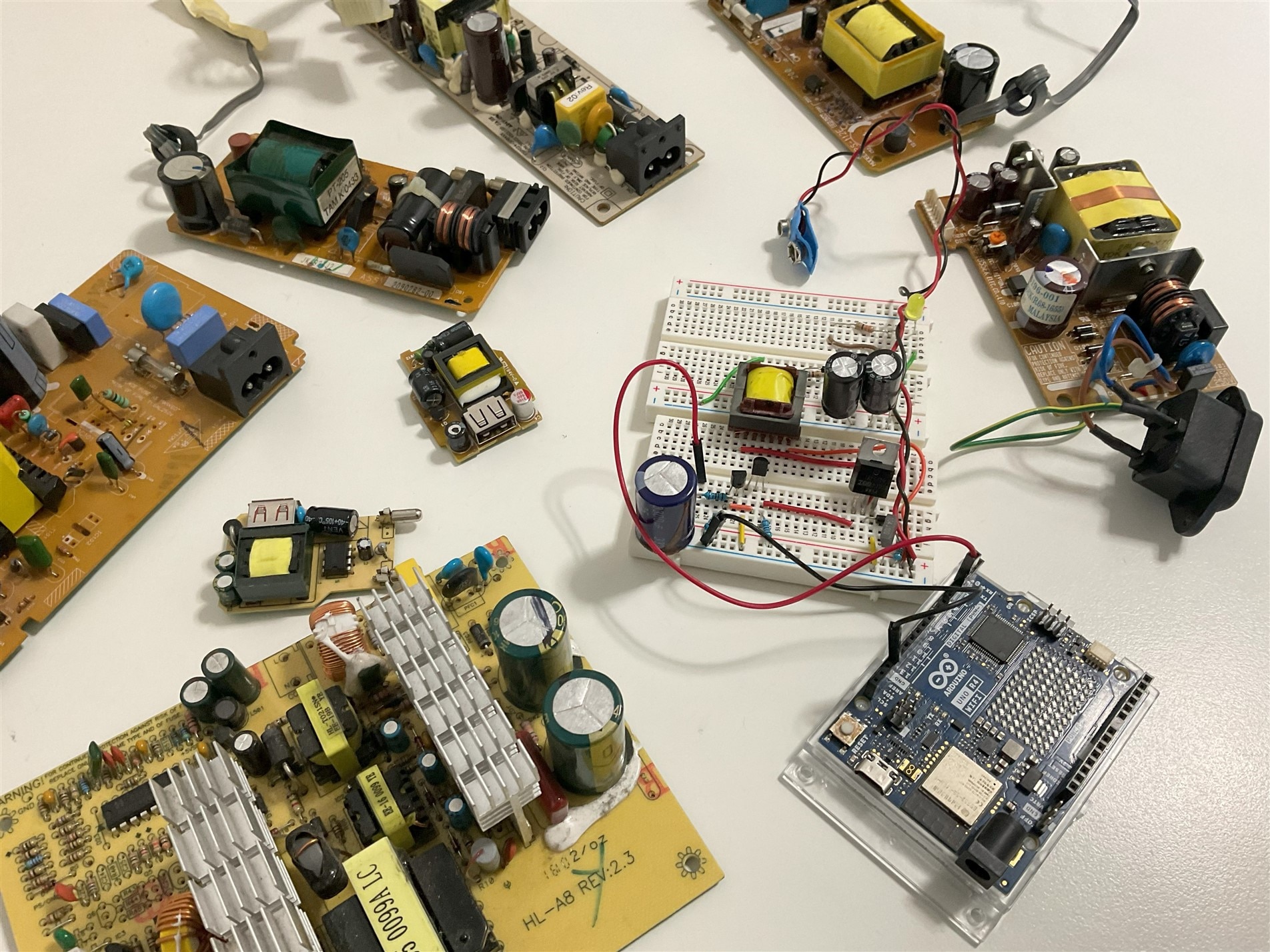
In the next image it is our experimental unregulated flyback switched mode converter surrounded by several comercial switched mode power supplies from abandoned printers, scanners, mobile chargers and PC power supplies. Switching power supplies are totally ubiquitous, they are in many electronic devices.
Regulation in flyback converters
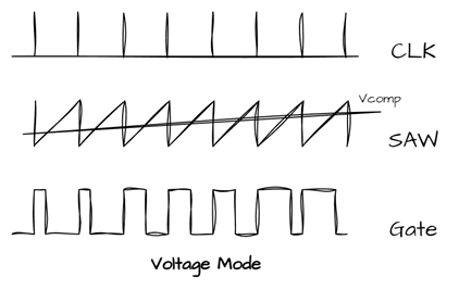
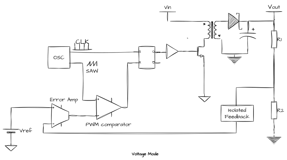
There are a couple of ways to go about it. You can use traditional PWM (Pulse-Width Modulation), either in voltage mode or current mode, where a free-running oscillator takes charge and controls the show. On the flip side, there are more budget-friendly designs where the transformer itself plays a role in a blocking oscillator. This setup helps save on a few components, making the design more cost-effective.
Voltage Mode PWM:
In voltage mode, we compare the integrated error signal (Verr = Vref − FB) with the oscillator's sawtooth waveform. What this means is that we're looking at the difference between a reference voltage (Vref) and the feedback voltage (FB). This helps us figure out how much adjustment is needed. Then, we compare this with a sawtooth waveform generated internally. This comparison helps control how long the switch stays ON.
Current Mode PWM:
In current mode, things work a bit differently. Instead of using a sawtooth waveform, we use the ramping current in the inductor. The internal oscillator still plays a role, but it's used to initiate each conduction cycle. This means it helps in starting the process rather than comparing with a sawtooth.
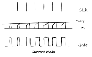
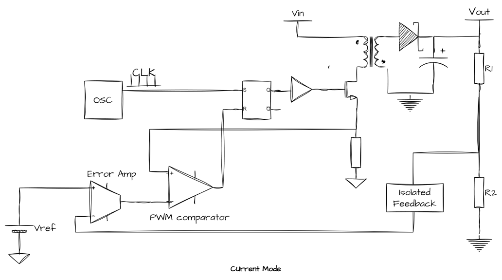
It's essential to note that both voltage mode and current mode are types of voltage regulators. The difference lies in how they use the error signal to adjust the pulse width, affecting how long the switch is ON.
My initial idea was to use a Hall-Effect-Based Linear Current Sensor IC to measure the current flowing through the load but the results at the moment are not satisfactory so I have relegated the tests of the regulation of the converter to a next blog.
Choosing the victim. Creatively torturing an SMPS transformer.
The first thing I had to do before starting the experiments on flyback converters was to choose a victim for them. My house does not meet the safety conditions to work with high power and to understand how flyback converters work you don't have to risk your life. My intention was to be able to start by carrying out small experiments with DC/DC converters using batteries as power sources.
Of the set of transformers in the kit, there is only one expressly designed to work as a DC to DC converter within fairly safe thresholds, the BA60951CS, but I wanted to save that transformer for the final project.
So I decided to choose another transformer that would allow me to use it creatively for the sole reason of better understanding how flyback converters work.
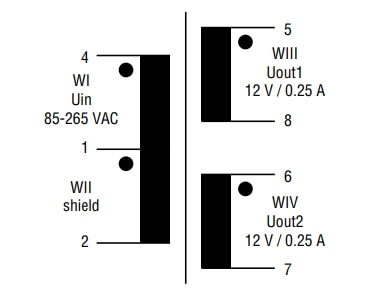
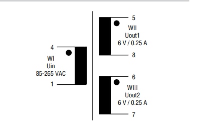
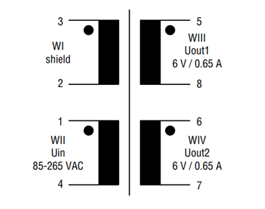
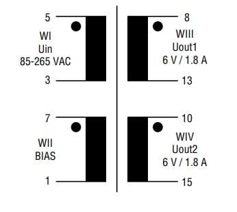
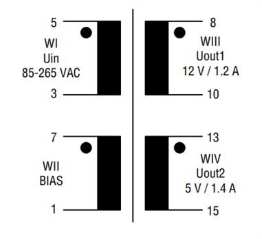
I relied on the following table to understand the different configurations of the windings of the different transformers and their transformation ratios.
|
|
|
 |
|
BA60951CS – Flyback Transformer wiring ratios: 1.27:0.77:1 |
063929 SMPS Transformer, Flyback wiring ratios: 18.6 : 1 : 1 |
063932 SMPS Transformer, Flyback wiring ratios: 10.6 : 6 : 1 : 1 |
|
|
|
|
|
093830 SMPS Transformer, Flyback wiring ratios: 4 : 18.5 : 1 : 1 |
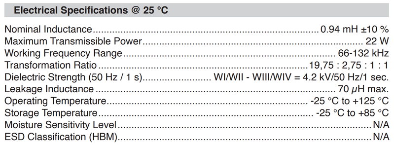
094931 SMPS Transformer, Flyback wiring ratios: 19.75 : 2.75 : 1 : 1 |
094932 SMPS Transformer, Flyback wiring ratios: 7.9 : 1 : 1 : 0.6 |
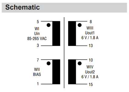
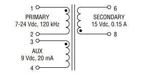
Some of these flyback transformers consist of an auxiliary winding which provides a low-voltage reference for control circuits as the 094931 SMPS Flyback Transformer.
Finally I selected the 094931 SMPS Flyback Transformer with the idea of using the BIAS winding as the primary, leave the actual primary unused and unconnected and the secondary windings, which have the same number of turns, to be able to use them individually, in series or in parallel. That gave me a lot of versatility to try different transformation ratios.
This decision has a serious problem and that is that the transformation ratio between the winding that I intended to use as primary and the real primary is 19.75: 2.75 in such a way that if I fed BIAS with 9 V it would have approximately 65 V in case of short circuit of the primary. Taking that into account and taking the necessary precautions so that this does not happen, I began the experiments with that transformer.
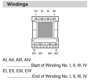
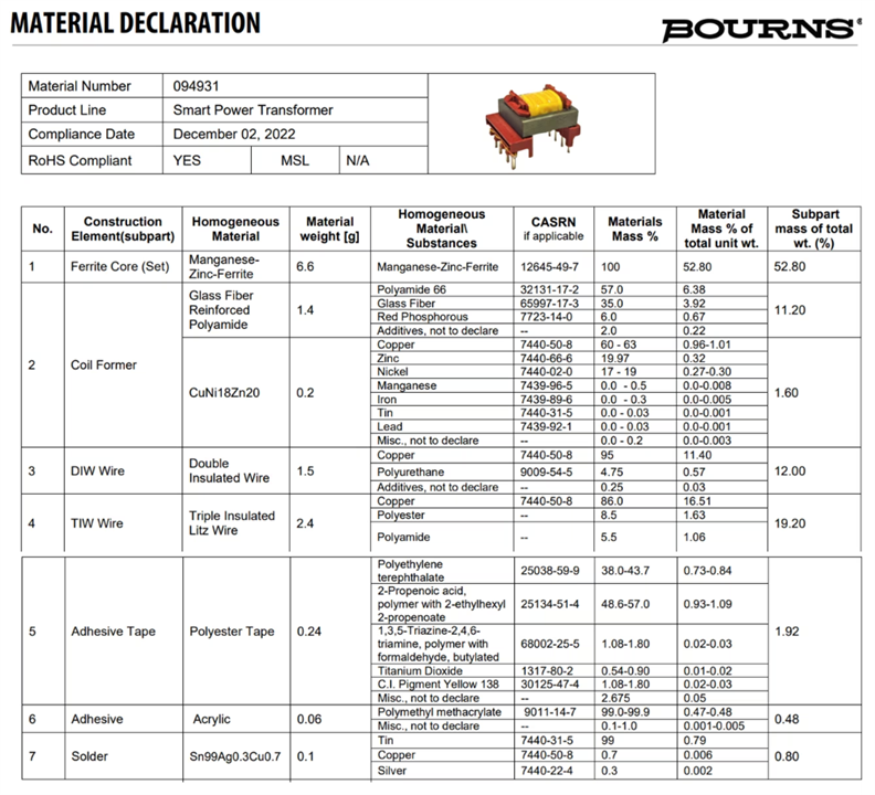
If you are curious about the materials used in the construction of this transformer, you can take a look at the Material Safety Data Sheet. An MSDS describes the properties and potential hazards of the material, how to use it safely, and what to do in an emergency.
https://www.bourns.com/docs/product-mds/094931_mds.pdf?sfvrsn=fd5158f6_5
Experiment 1: Working as a linear power transformer
Once I selected the transformer to be martyred, the first thing I worry about is learning to identify the different windings of the transformer. I didn't want to have surprises and find voltages higher than expected. So the first thing I tried is to work with the transformer as a linear power transformer with two of the windings chosen for the rest of the experiments. The BIAS winding and one of the two secondaries.
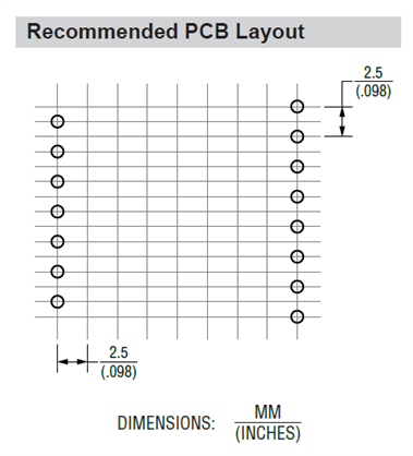
First problem: The pin spacing of this transformer is not suitable for working on a breadboard, I understand that for safety reasons. To be able to work with a breadboard environment, I used two breadboards, one without one of the power strips. In such a way that the inputs and outputs of the primary windings of the transformer rest on a breadboard different from the breadboard where the inputs and outputs of the secondary windings rest.
There is a good separation between both breadboards.
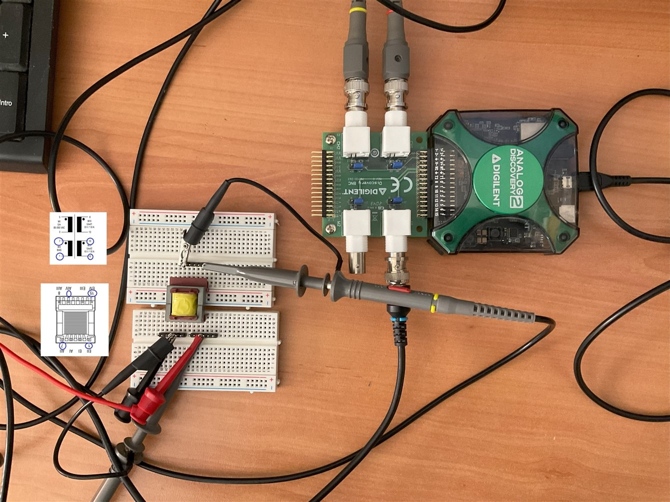
For this first experiment I used the wave generator and the oscilloscopes of the Digilent Analog Discovery 2, always with small signals and low currents.
Response to sinusoidal wave:
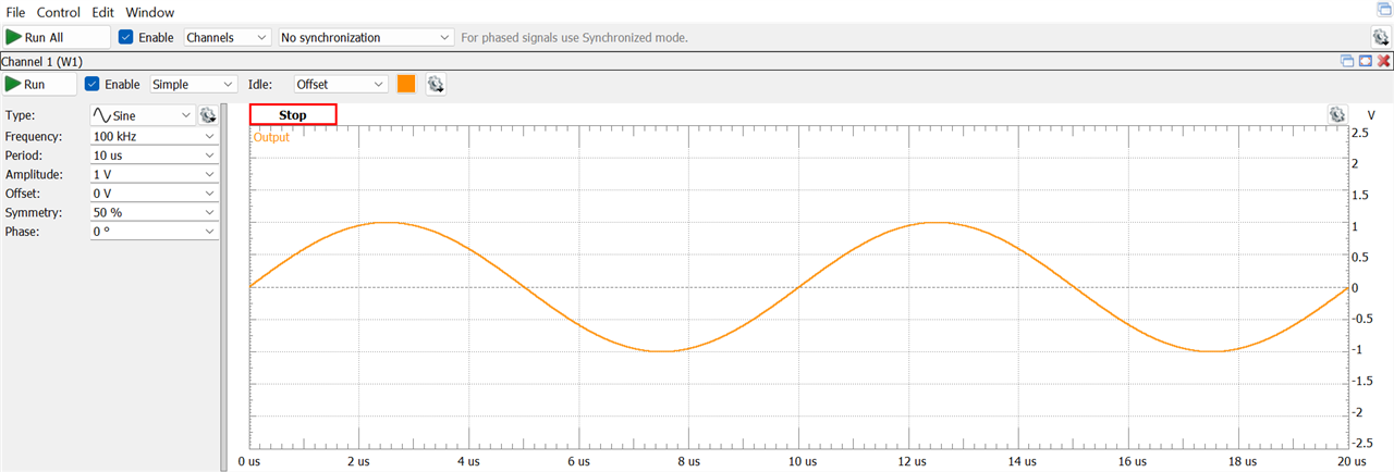
Using the wave generator I applied a 100 kHz 1V signal to the BIAS winding
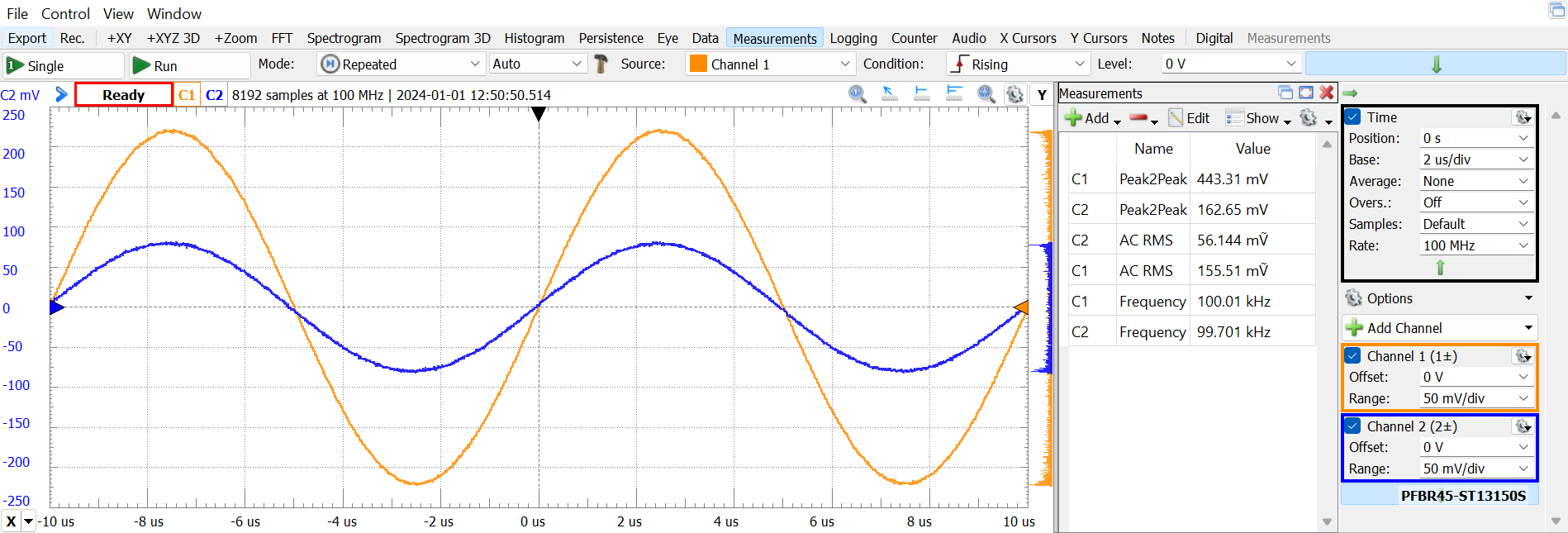
We can try to calculate the turns ratio between the two windings using the Peak2Peak measurements
443.31 / 162.65 = 2.72 That's very close to the 2.75 indicated on the data sheet.
In the graph we can also see that the chosen polarities of the two windings are in phase and coincide with the references chosen with the two probes of the two-channel oscilloscope.
With this small experiment we have been able to check the turns ratio of the two windings, identify our primary and secondary for the rest of the experiments and the polarities of both windings.
Experiment 2: Pulse response
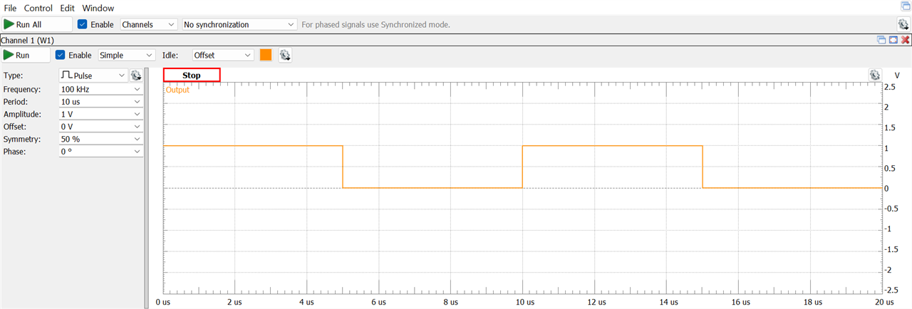
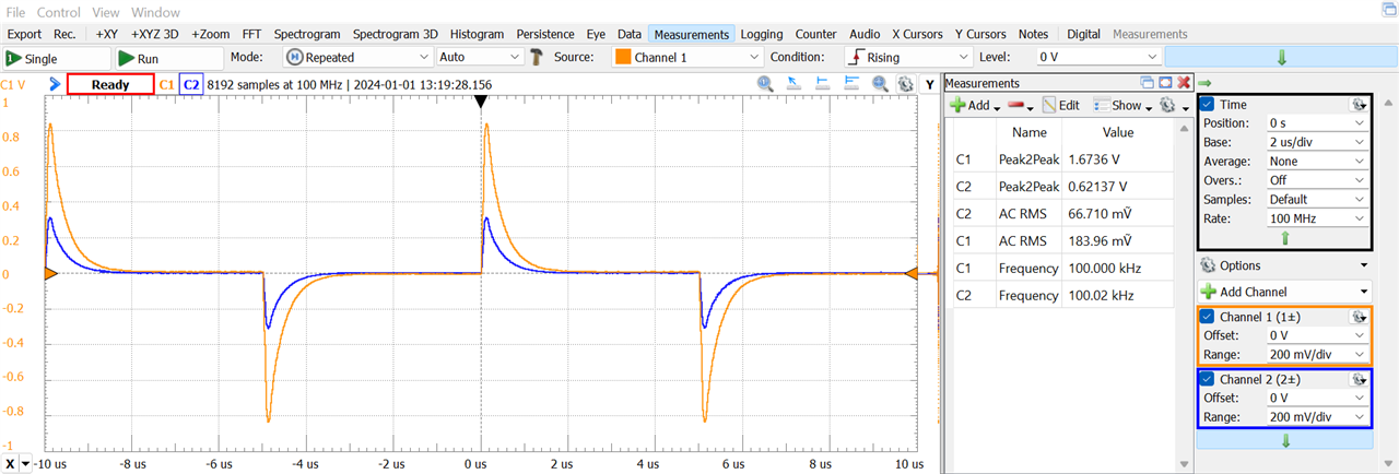
After verifying that it was working with the chosen windings and well identifying the polarities of the two windings, I proceeded to treat the response of the transformer to different pulses of different widths at the frequency of 100 kHz.
Pulse response. 100 kHz PWM signal 50% duty cycle.
Experiment 3: Pulse response, secondary rectifier diode and capacitor
For this experiment I connected a 1N5819 Schotty fast switching diode to the secondary of the transformer and a 470 uF electrolytic capacitor.
We are getting closer to the typical configuration of a flyback DC/DC converter.
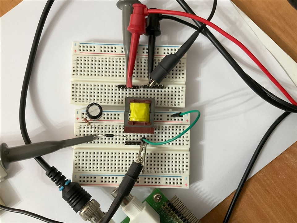
The load is a 2K2 resistor. For these experiments I had to increase the amplitude of the pulses so that the diode could switch to conduction in the off phases of the switch.
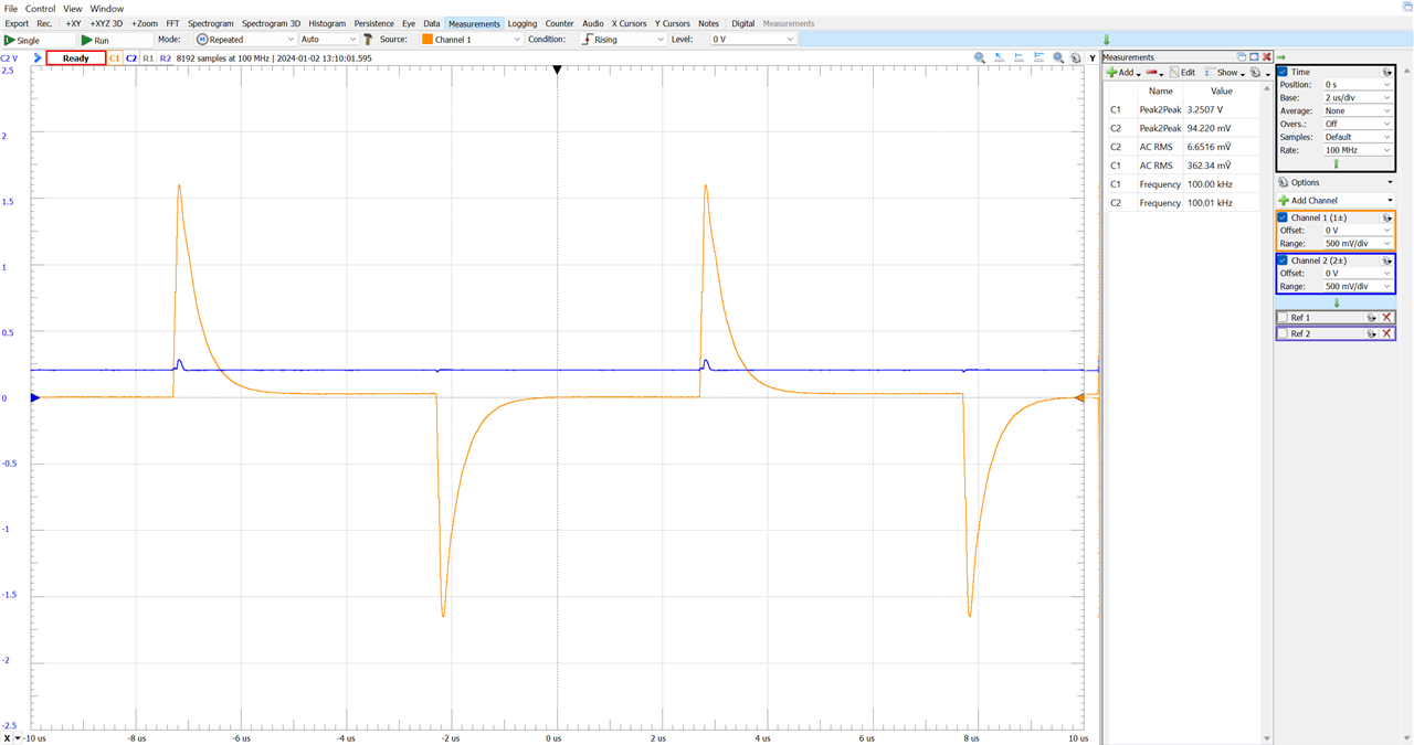
I tried different pulses of different widths at a frequency of 100 kHz.
We already have a DC output at the output of this simple converter.
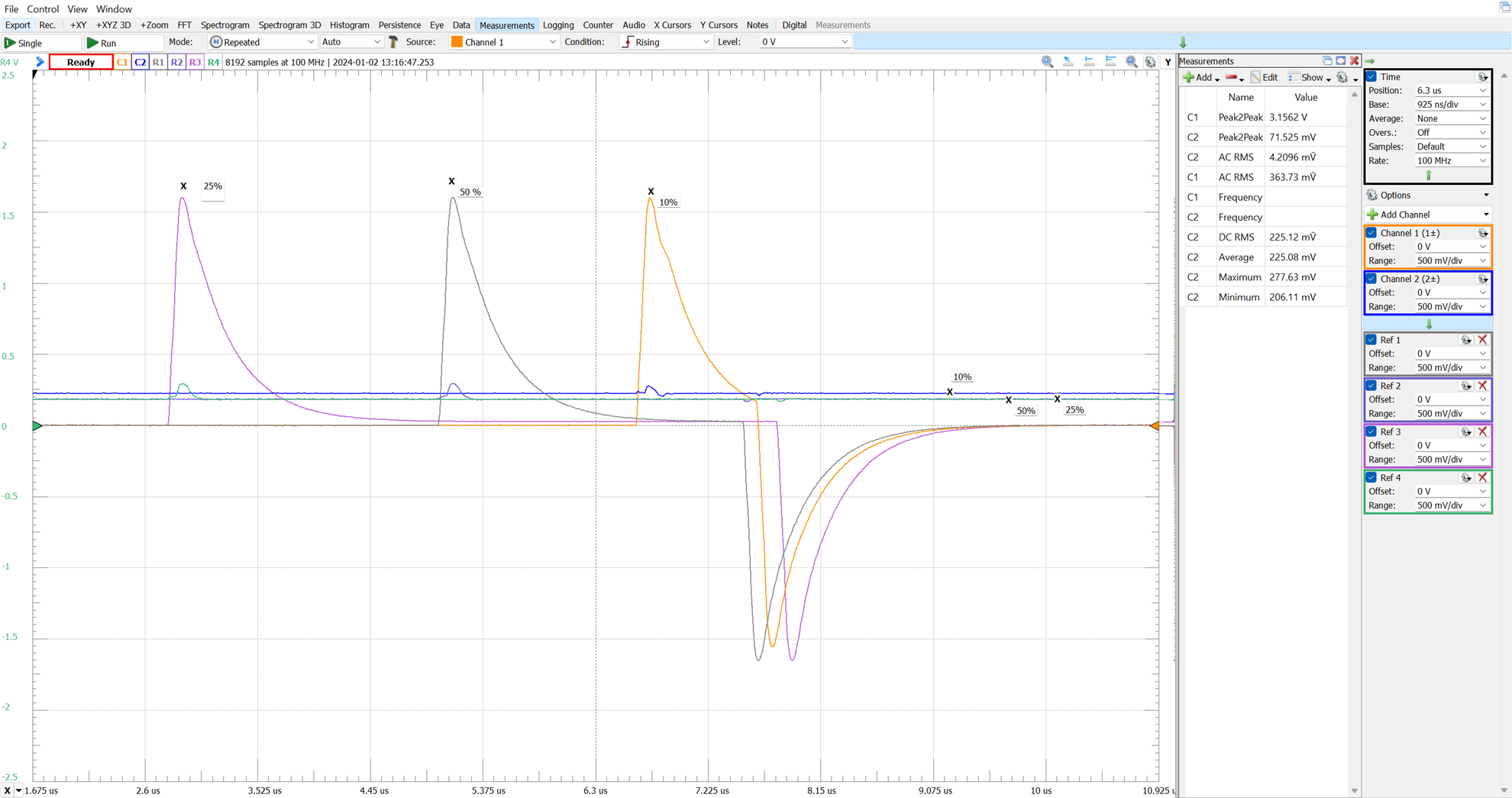
In the video you can see the response while changing the pulse width, with a limit of 50% duty cycle.
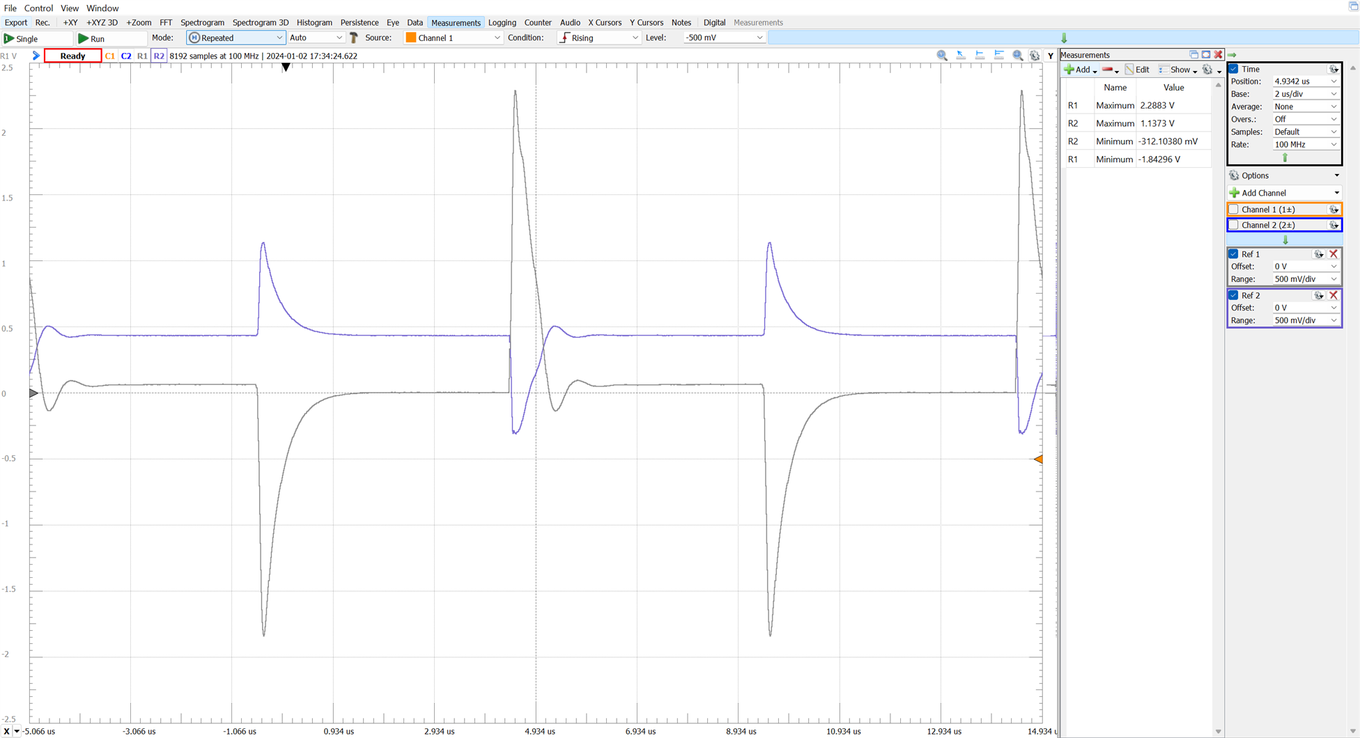
Voltage across diode.
Experiment 4: Generating a 100 kHz PWM signal with a microcontroller.
To control the converter I was not going to use a commercial controller IC since for the final project I want to control the converter from a microcontroller. I have several development boards with different microcontrollers but I decided to use an Arduino UBO R4 WIFI that Arduino sent me to test.
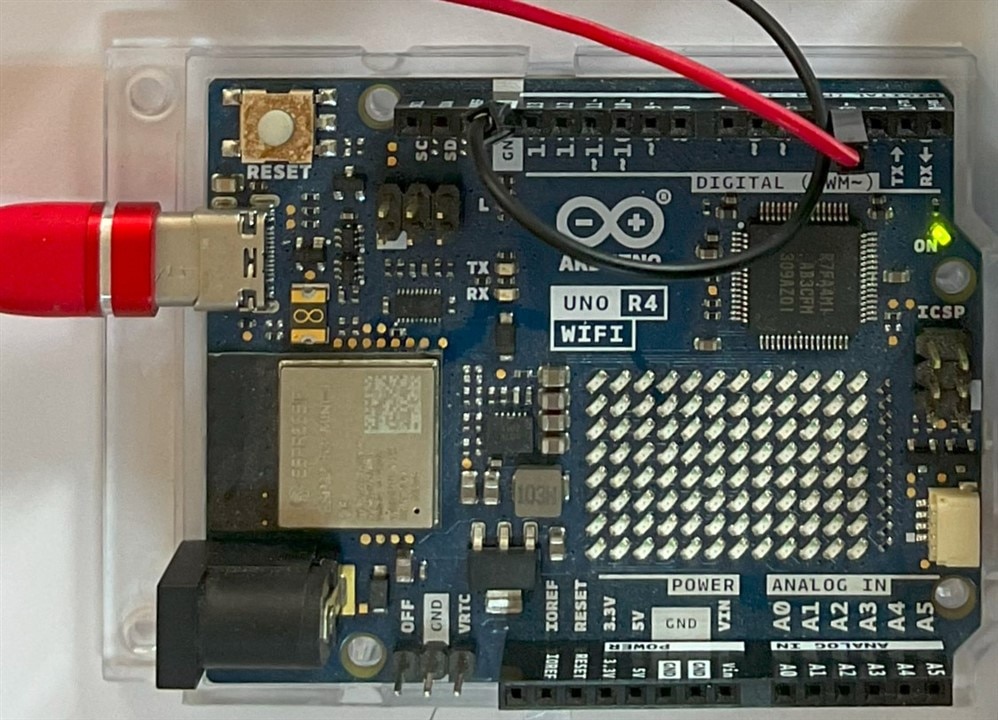
Arduino R4 WIFI
Generating a 100 kHz signal with the Arduino R4 is straightforward. You just have to include the "pwm.h" header and instantiate a PwmOut object on the port on which you want the PWM signal to be generated, D3 for our experiment. To indicate the frequency we call the begin function giving the signal period, 10 us in our case for a frequency of 100,000 Hz,
100 kHz = 10 µs(p)
Sketch for generating PWM signal with the Arduino R4 WIFI
#include "pwm.h"

PwmOut pwm(D3);

void setup() {
  //period 10us = 100 000hz; pulse 0 us = 0%
  pwm.begin(10, 0.0);
}

void loop() {
  float percentage = 0;
  for (int i = 0; i < 7000; i++) {
    percentage += .01;
    pwm.pulse_perc(percentage);
    delay(1);
  }
  for (int i = 7000; i > 0; i--) {
    percentage -= .01;
    pwm.pulse_perc(percentage);
    delay(1);
  }
}
The following video shows the output of the arduino when the previous code is run that varies the width of the PWM signal sequentially.
Experiment 5: Using an optocoupler to drive the MOSFET switch from the microcontroller
I wanted to do tests with a MOSFET, I didn't have any MOSFET on hand that works as a switch with the logic levels of the Arduino so I thought it was a good idea to try building a MOSFET control circuit that will isolate the MOSFET from the driver circuit using an optocoupler. The PC817 optocoupler is an optocoupler that is present in many power supplies that I have disassembled so I thought it would be a good candidate.
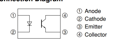
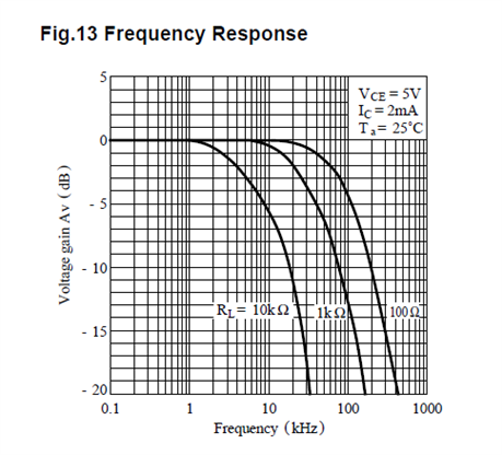

After reviewing the data sheet I saw that it was not a good option for 100 kHz and above frequencies, but it was all for science and learning something, I gave it a try.
I used a (5 V - 1.2 V) / 20 mA = 180 Ohm resistor for limiting the diode current
6 kHz VCE 9V R= 1 kOhm on the left image and 100 kHz on the right image
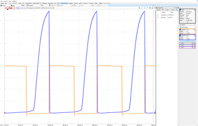
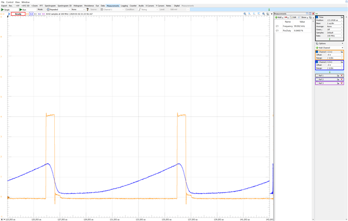
This was definitely not the way to go.
Experiment 6: Using BJT transistors to drive the MOSFET from the microcontroller
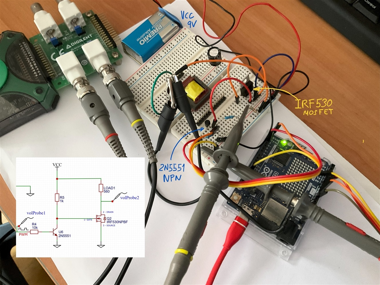
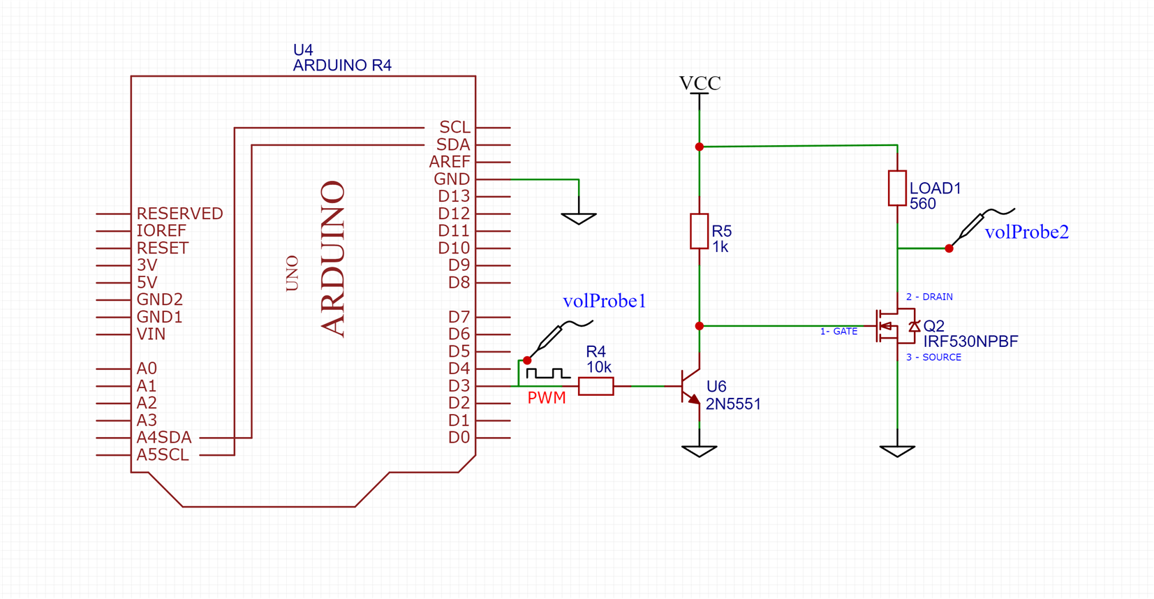
Once the optocoupler option was discarded, I thought about making a driver circuit with a gate isolation transformer, using a Bourns pulse transformer. I left this exercise for a later blog. The next option was to build a driver circuit with two NPN BJT transistor-based inverters. I used two NPN 2N5551 transistors
https://es.farnell.com/on-semiconductor/2n5551/transistor-npn-160v-to-92/dp/9846751
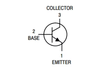
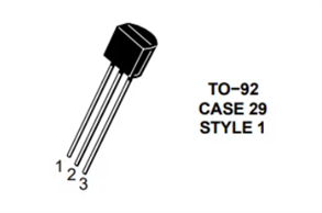
From the experiments in the previous blog we saw that 100 kHz was a suitable frequency to work with the transformer selected for these experiments. At this higher frequency, switching losses become significant, making it crucial to find a MOSFET that balances low gate charges, low on-resistance (RDS(on)), and high efficiency. Gate charge (QG) is a key factor influencing a MOSFET's ability to switch on and off rapidly, vital for hard-switching applications. The MOSFET figure of merit (FOM) is often expressed as RDS(ON) * QG, where lower values indicate better performance.
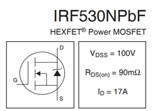
Of the MOSFETs I had on hand, the one that seemed best for these experiments was the IRF530NPbF HEXFET Power MOSFET. It is a TO-220 package MOSFET, for these frequencies a quad-flat no lead (QFN) package would have been better, but my intention for this blog was to work with breadboards although that they are also not recommended for high frequencies.
IRF530NPbF: RDS(on) = 90mΩ, Qg Total Gate Charge 37 nC
This is the circuit used:
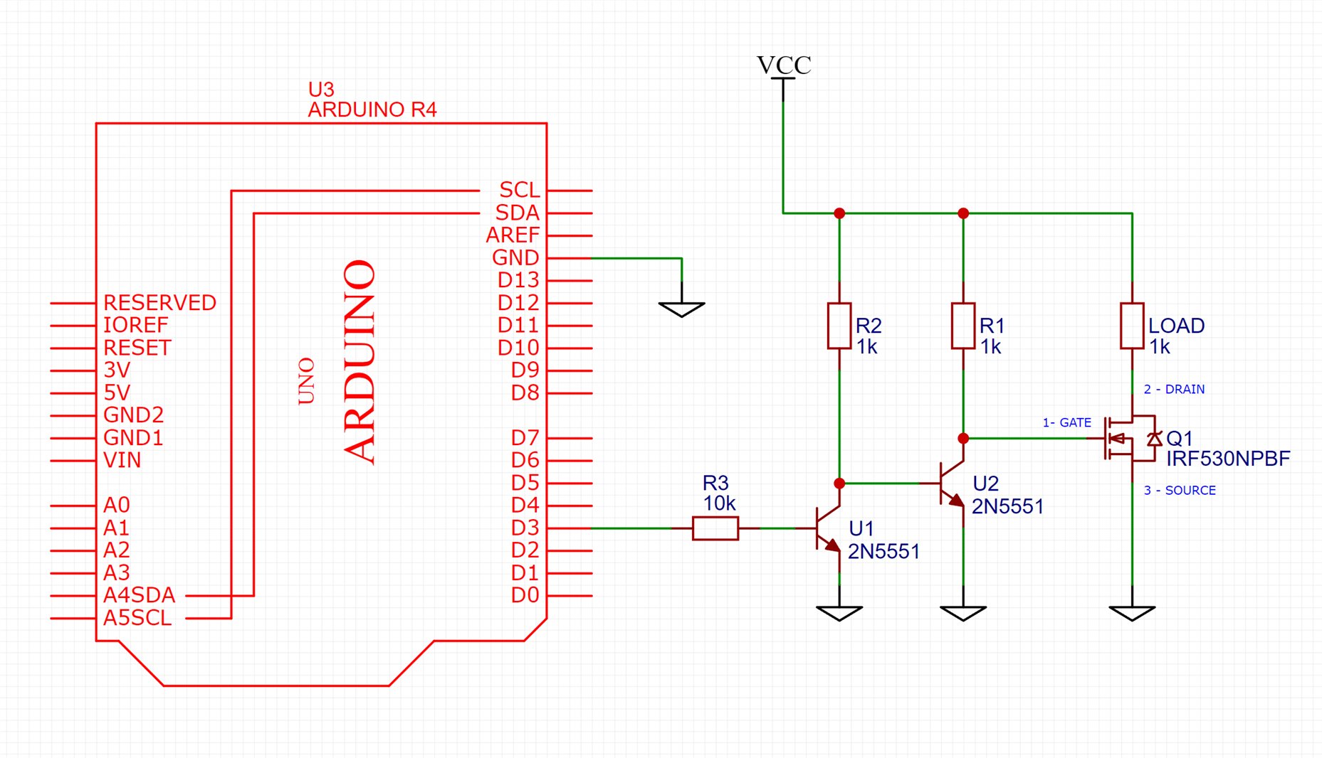
one BJT RBase 10K R Collector 1K, Vcc 9V DC
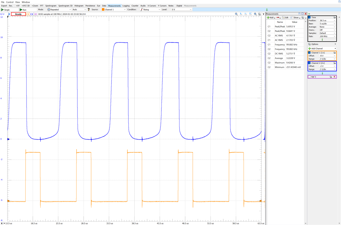
After tweaking pos duty range
#include "pwm.h"

PwmOut pwm(D3);

void setup() {
  pwm.begin(10, 0.0);
  pwm.pulse_perc(50.0);
}

void loop() {

  float percentage = 0;
  for (int i = 0; i < 3600; i++) {
    percentage += .01;
    pwm.pulse_perc(percentage);
    delay(10);
  }
  for (int i = 3600; i > 0; i--) {
    percentage -= .01;
    pwm.pulse_perc(percentage);
    delay(10);
  }
}
Experiment 7: Blindly and Erroneously Optimizing the MOSFET driver.
As a computer programming man, I thought I could save a transistor in the MOSFET driver circuit. If the PWM signal was inverted at the output of the first transistor, I would make the change through software. And so I did it, without thinking about the consequences. I didn't realize that in this way, in the absence of a PWM signal, the MOSFET would be in the ON state and direct current would circulate through the primary of the transformer being able to destroy it.
I carried out several experiments, here are some results and fortunately I did not have the transformer subjected to direct current and high currents and nothing broke. But, please, don't do that.
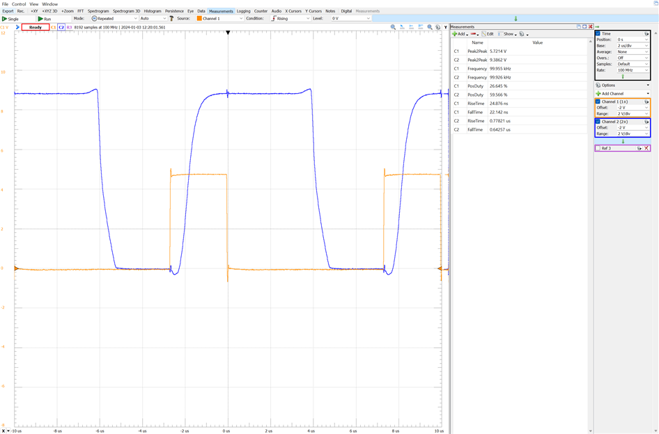
I started by checking this circuit, that gave me false confidence.
Vds and PWM Signal at 100 kHz
It seemed to work fine.

Experiment 8: 1st Don't Try This. Flyback converter without primary snubber.
Excited by the previous results, I decided to optimize ahead of time without taking into account that I could destroy the transformer due to carelessness or an unexpected software error.
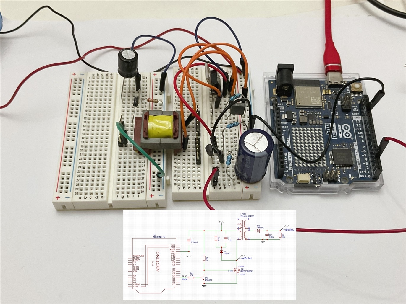
First I carried out tests without the snubber RCD network, I wanted to see those voltage peaks that I had read so much about, I was not worried about losing this MOSFET since I have several more and science was the most important thing at that time. Fortunately nothing broke.
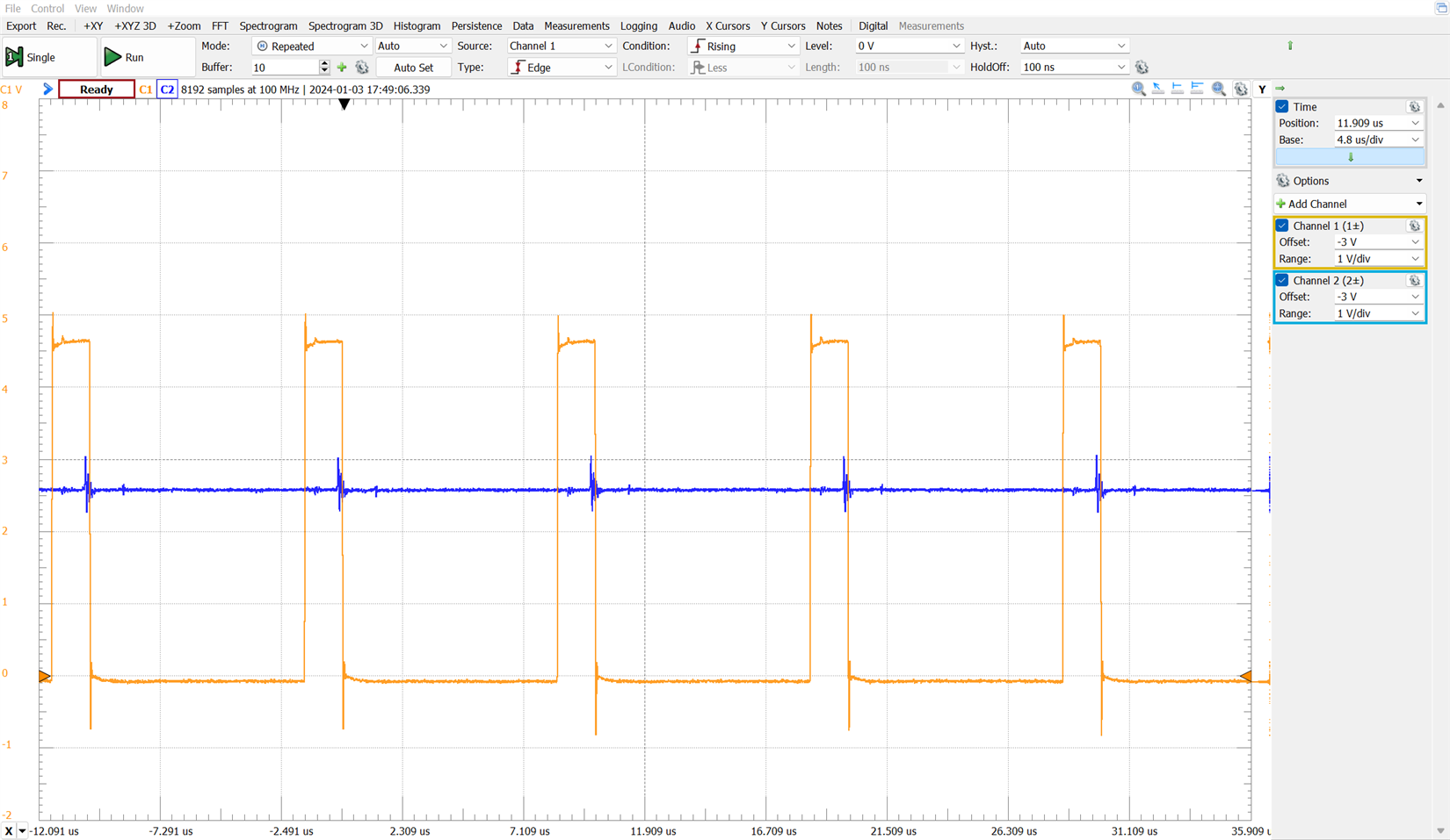
Everything seemed to be going correctly. In the image the PWM signal of the Arduino and the output of our unregulated source outputing 2.6 VDC
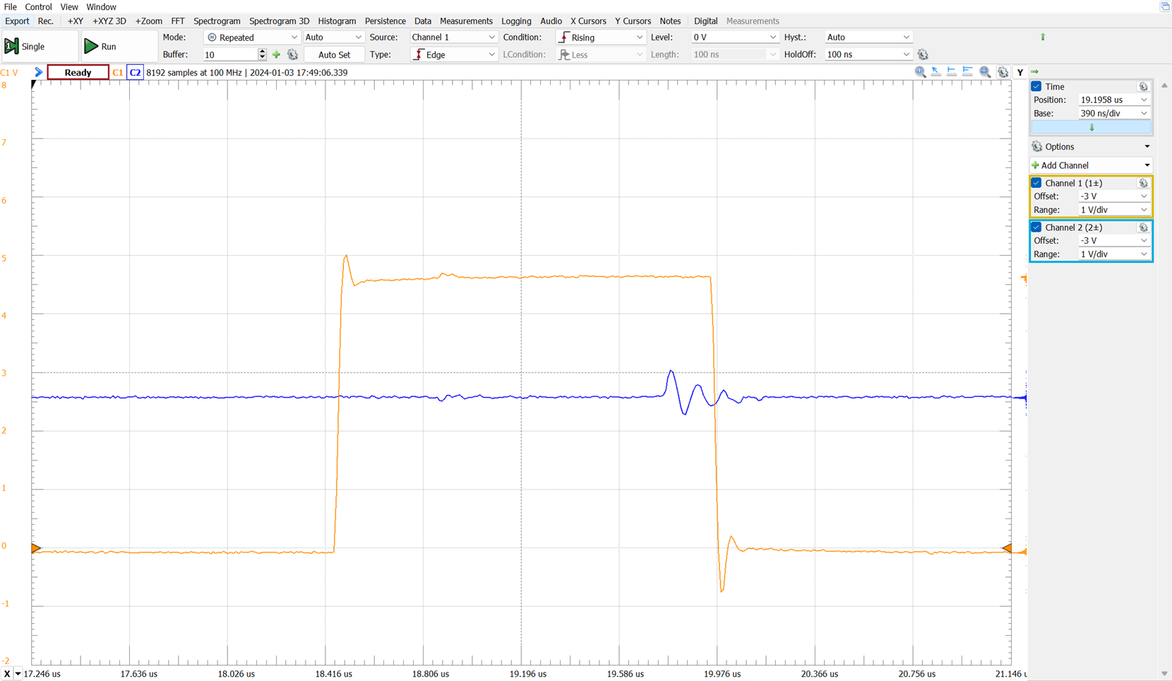
By zooming in on both signals we can see a small resonance in the output signal.
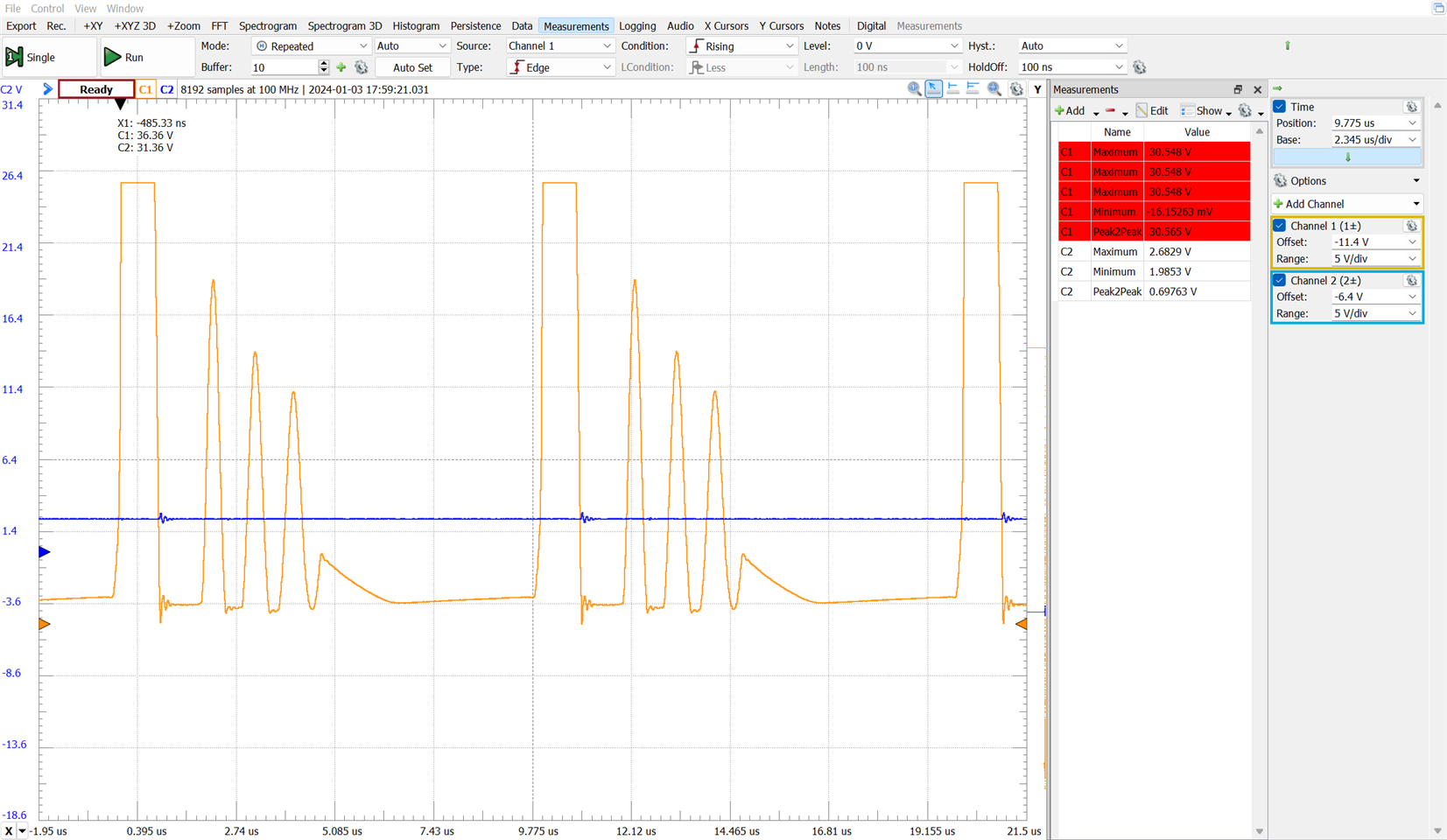
But when I went to analyze the voltage on the MOSFET Drain terminal I got a little scared. There was no attenuation on the probe and there were 30 volt spikes. Everything in red, bad symptom.
Vds over the range limits for x1
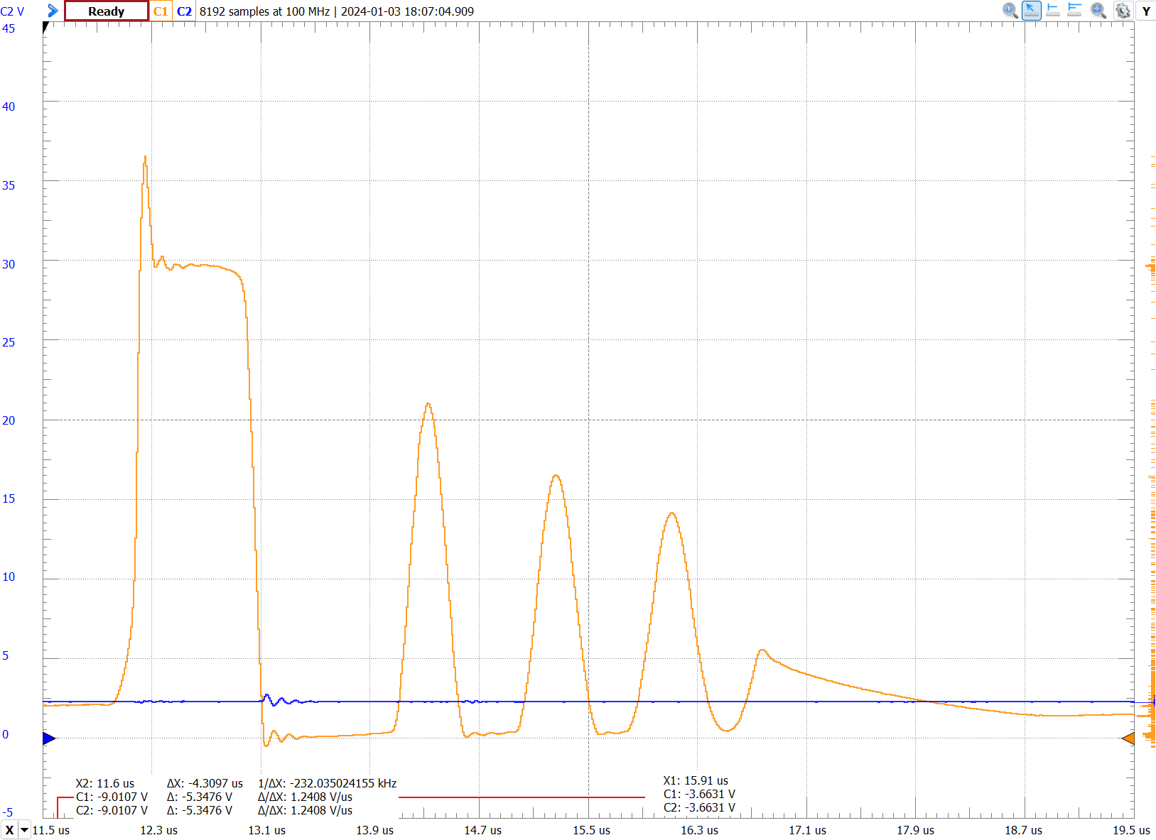
By attenuating the signal with the probe in position x10 I was able to observe the reasons for the snubber network in the primary.
x10 Attenuation. VDrain
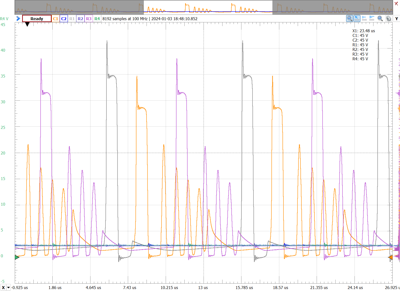
At different duty cycles it went even worse: 5% 15% 20% PWM Duty cycle. 45 VDC
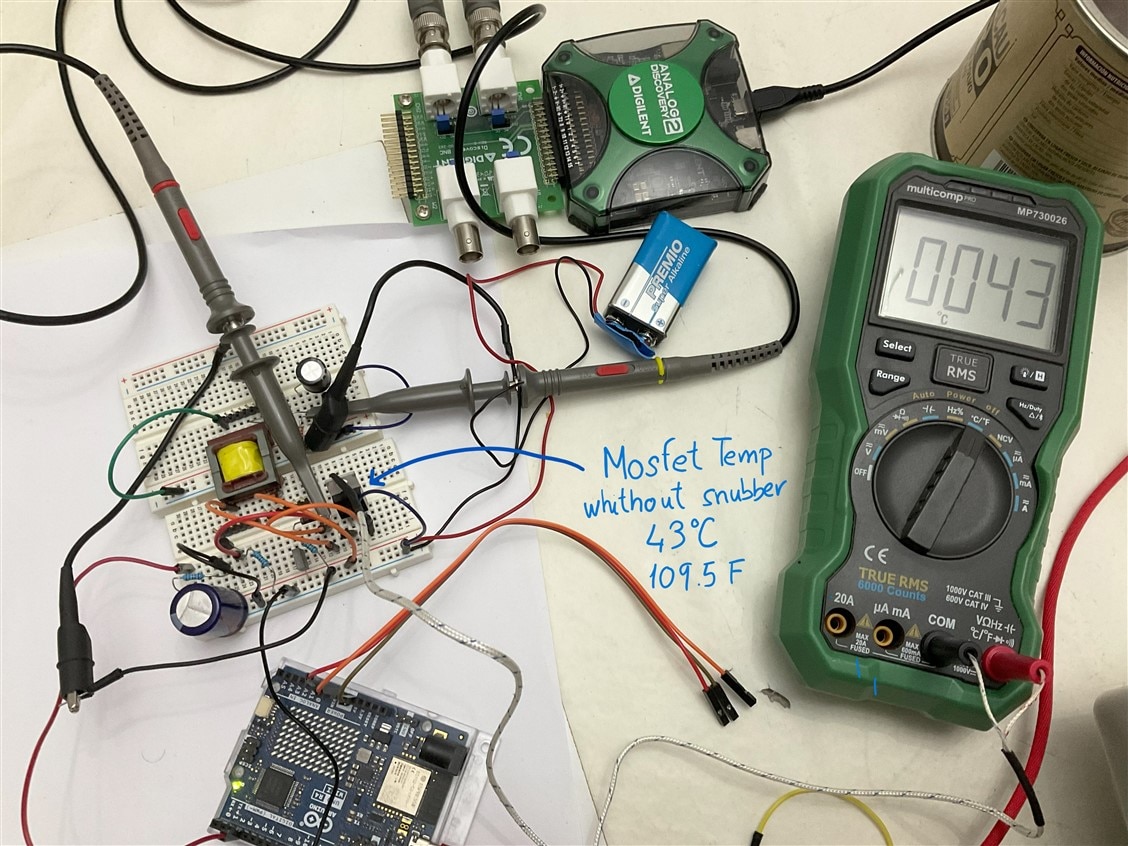
The MOSFET started to heat up. 43 °C The temperature in the room was 6 °C with the windows open.
Experiment 9: 2nd Don't Try This. Flyback converter with primary snubber.
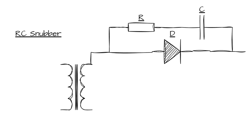
Ideally, when the MOSFET turns OFF in the flyback converter, all the current from the primary side should smoothly transfer to the secondary side, and everything would be fine. But, in the real world as we have seen in the previous experiments there's a hitch. The incomplete connection between the primary and secondary sides creates what it is called "leakage inductance." This leads to a bit of an issue: a positive voltage spike at the switch, even though the secondary side is under control. Not ideal. To fix this, we can use something called a snubber network. This could be a simple RC (resistor-capacitor) combination across the winding, or, for a more effective solution, a "DRC" network involving a diode in series with a parallel RC. This helps to keep things smooth and prevent unwanted voltage spikes.
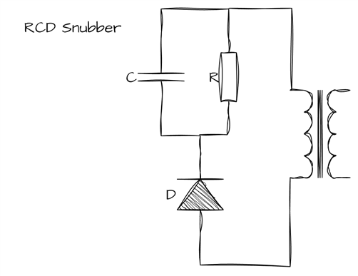
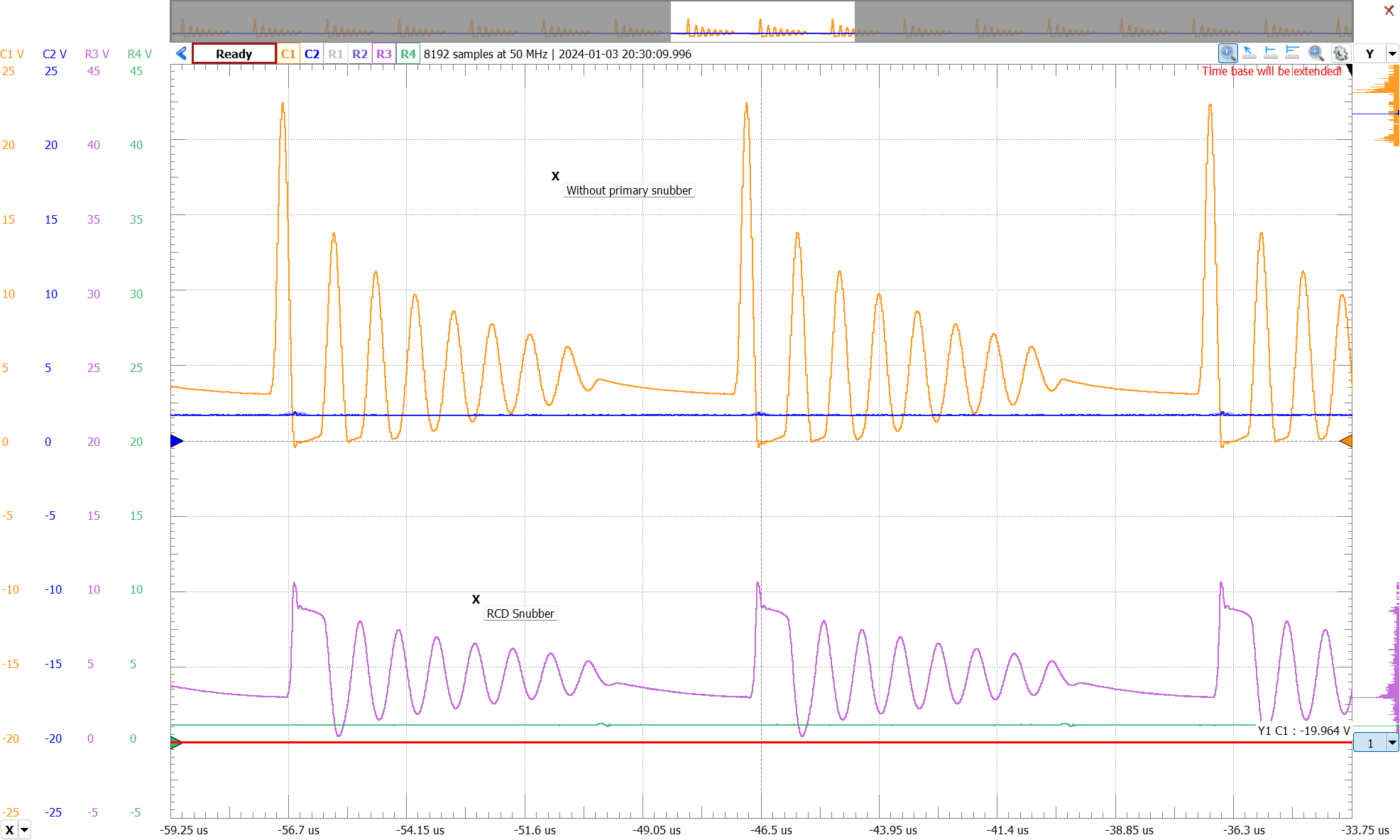
I did tests both with a snubber circuit in the primary and without it to check the voltage spikes and their mitigation by the snubber network.
RC Snubber for the secondary diode
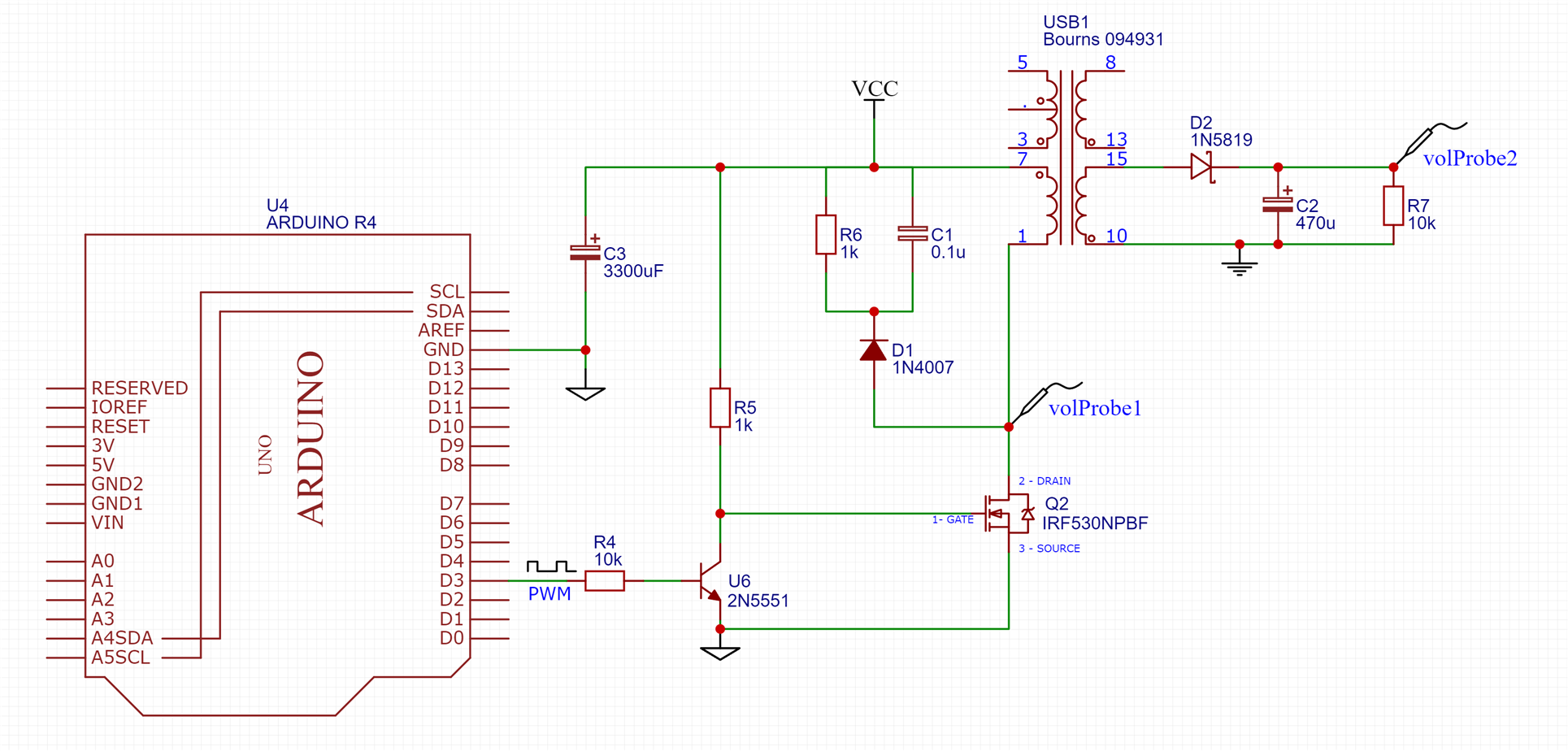
This is the circuit I used to check the effects of the primary snubber network. Again the warning that this circuit could damage the primary of the transformer by having the MOSFET on when the PWM signal is not present.
The snubber network consists of a fast rectifier diode and a parallel RC circuit in series with the diode.
The snubber circuit really worked.
This is the voltage on the mosfet drain over time for various duty cycles of the pwm signal.
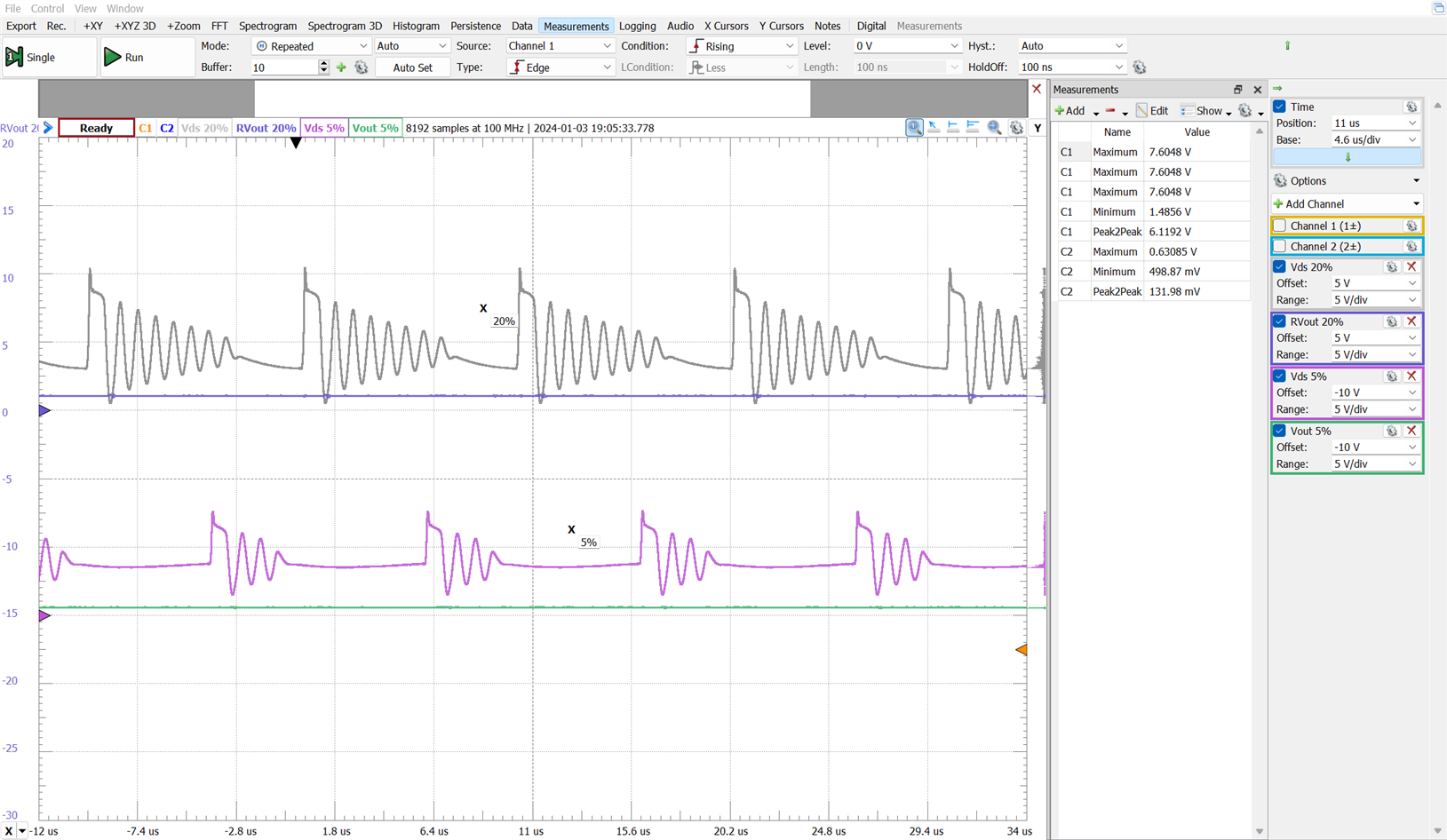
The temperature in the MOSFET dropped to 22 degrees with the room at 16 C.
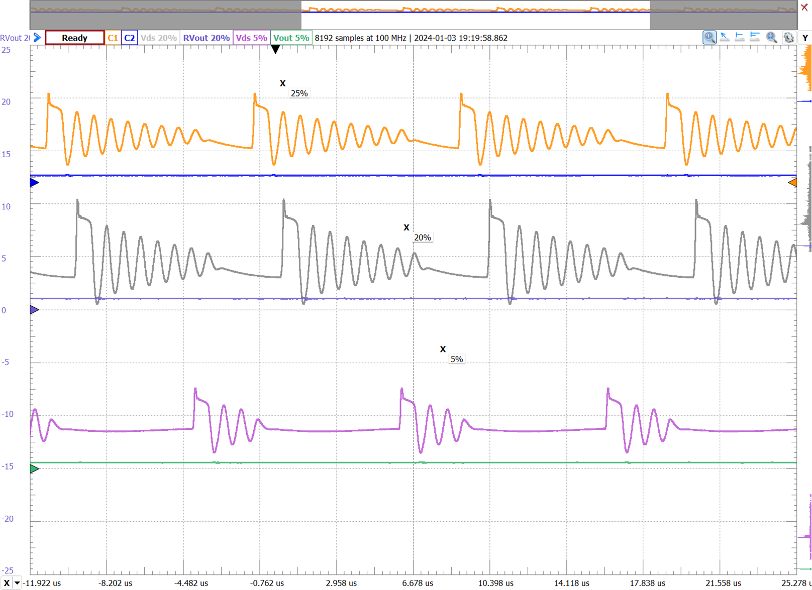
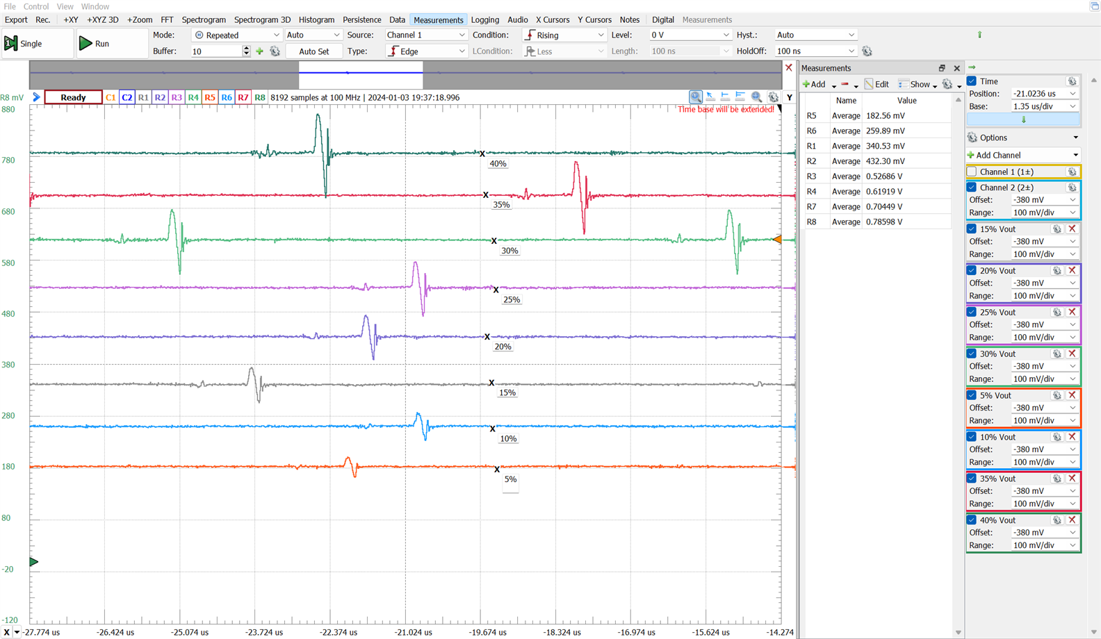
Vout for different duty cycles
Comparing Vds with the primary RCD snubber and without it. The snubber circuit is doing its job. I have to learn how to improve these results in a more scientific way and not in a totally experimental way.
Experiment 9: Gluing it all together my first unregulated DC/DC flyback converter.
Finally, to finish, I present the latest design of our experimental unregulated DC/DC flyback converter and the latest tests carried out with it.
As shown in the first image of this blog, here is the final circuit with which I concluded my first experiments with the DC/DC Flyback Converters.
The components used in snubber network circuits require a complex study that exceeds the motivation of this blog. I have had fun making many combinations of different component values but right now I do not have the necessary knowledge to be able to give a complete explanation of them. the results. There are too many parasitic factors, parasitic inductances and capacitances caused by the type of breadboard construction to be able to draw conclusions about the results.
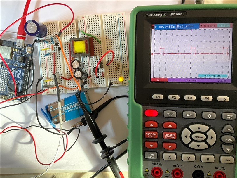
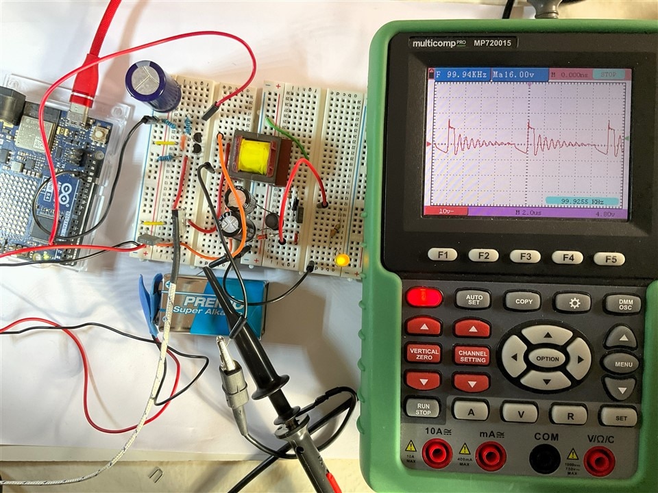
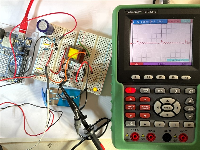
Output Signal: I think there is a little oscillation due to some resonance caused by parasitic inductance and capacitance. I need to study more about this.
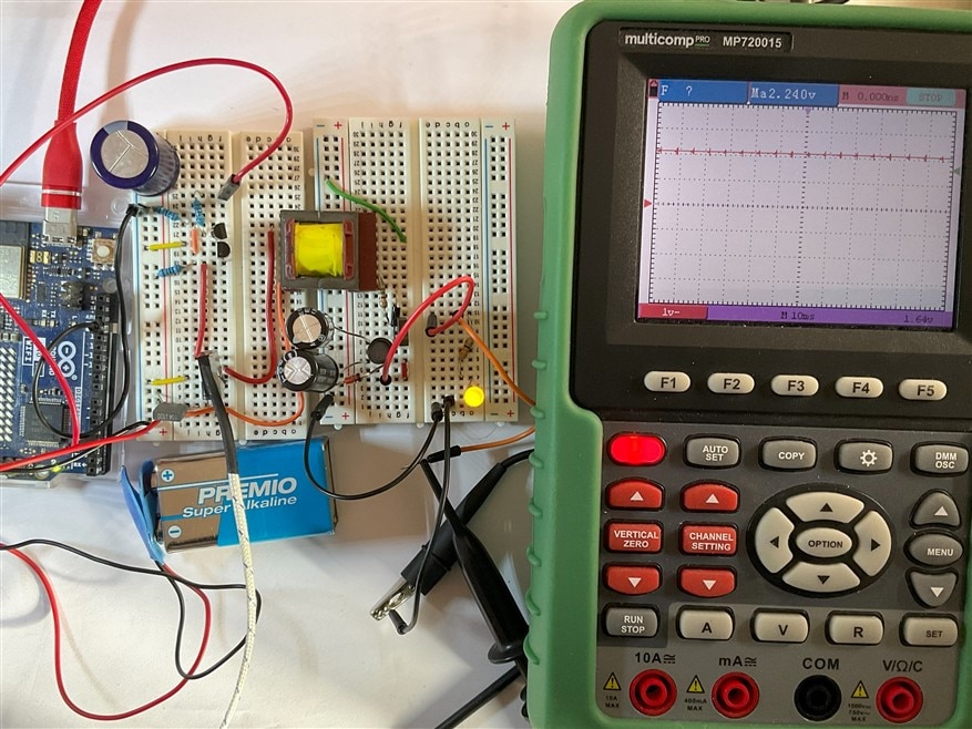
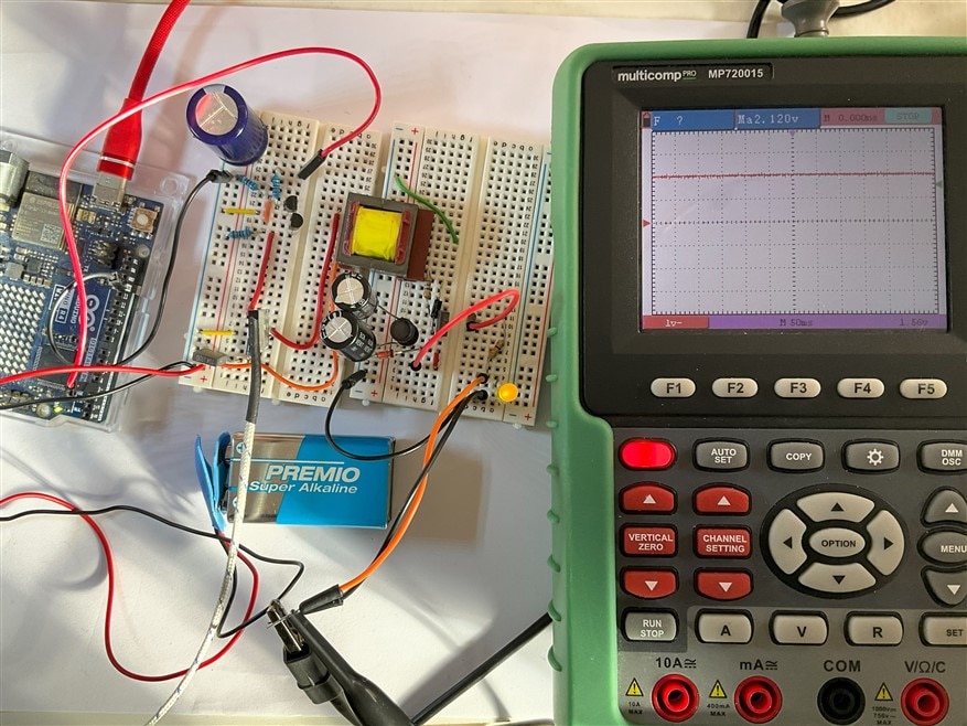
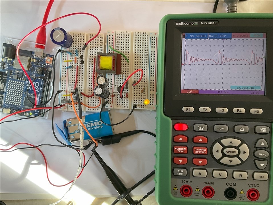
MOSFET Drain Voltage Signal. Max 22.40V. The good influence of the RCD snubber network is noticeable.
Arduino PWM Output for 100 kHz
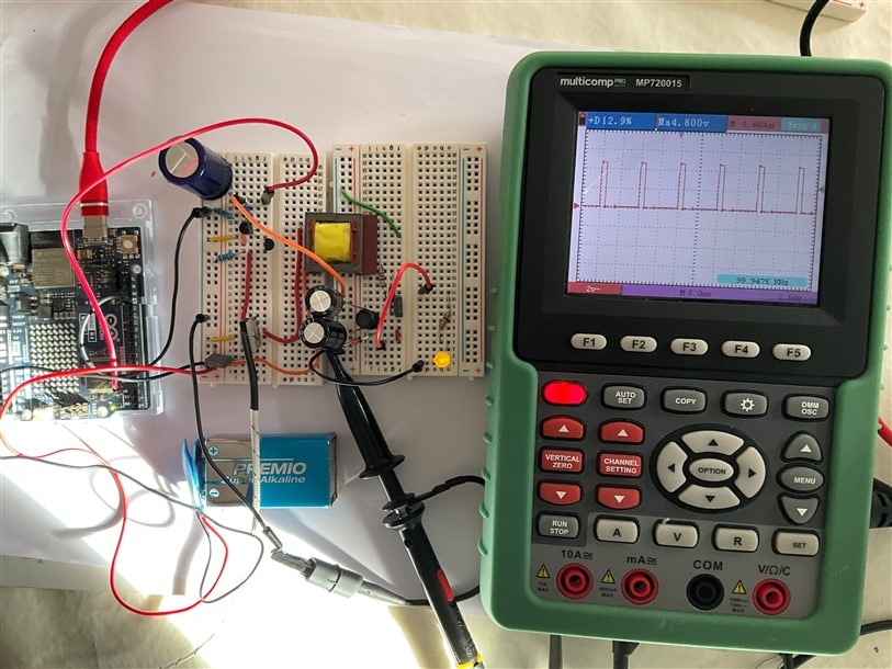
Voltage across secondary Schottky diode
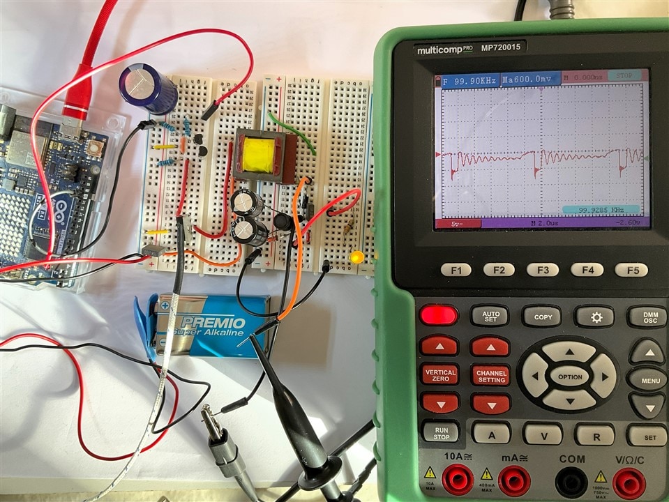
Voltage across Transformer Primary. The good influence of the RCD snubber network is noticeable. And voltage across Transformer Secondary
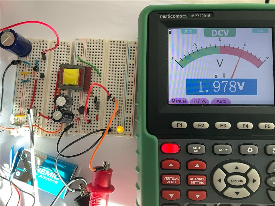
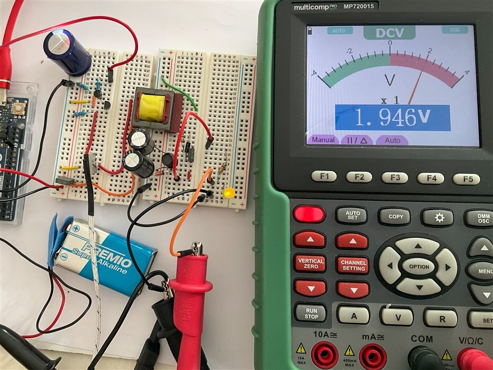
Voltage supported by the diode: 1.946 V
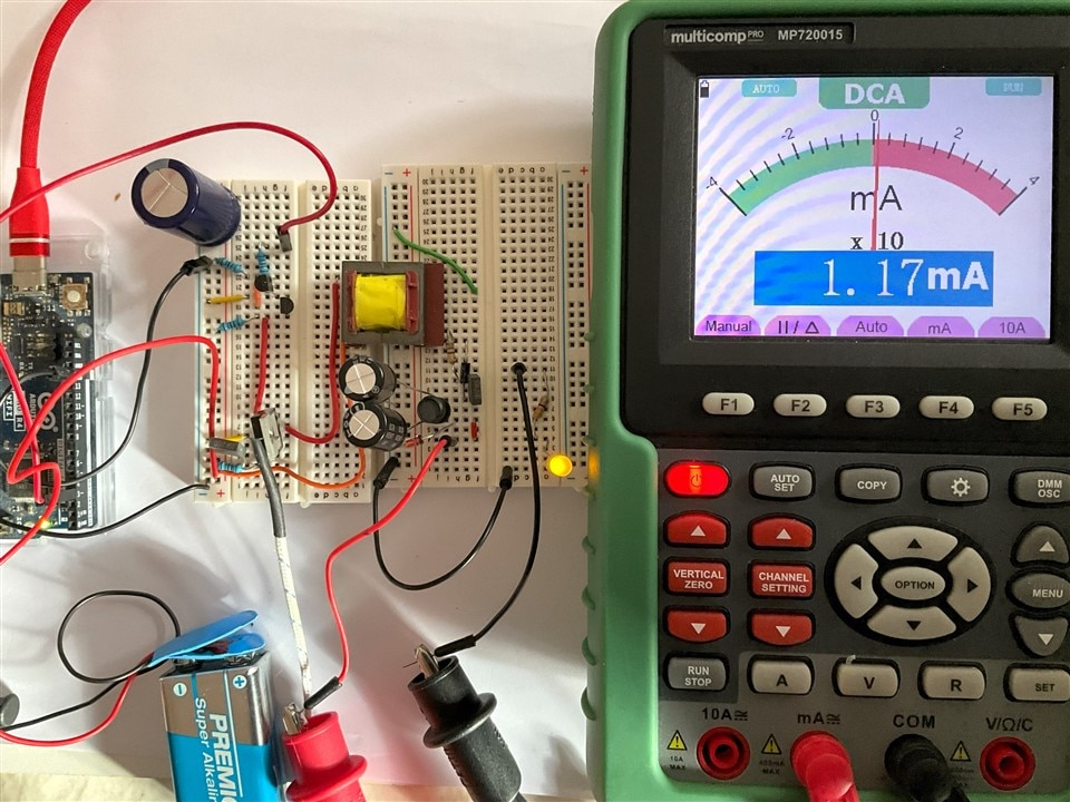
Input Current: Current measured at the positive connector of the 9V battery, 36.42 mA
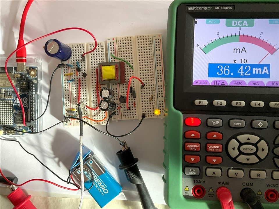
Load current: A small 38 Ohm resistor is limiting the current through the diode.
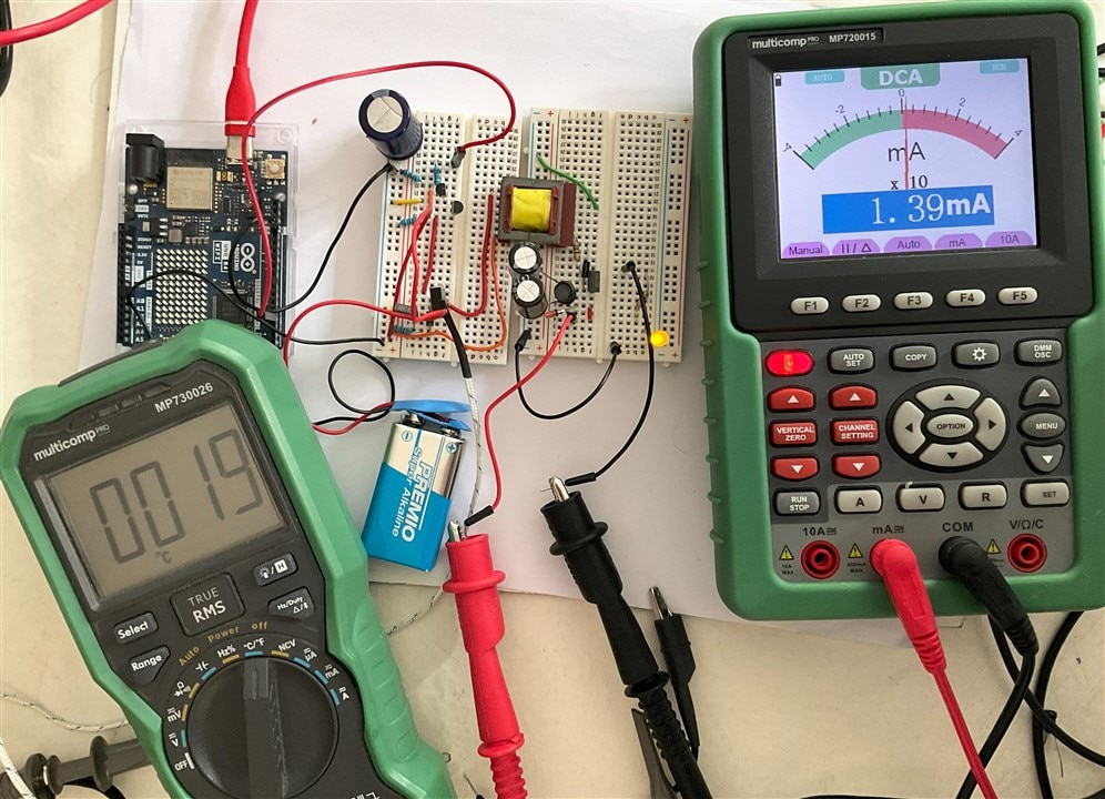
The temperature of the MOSFET is 19 C, the same ambient temperature, very far from the 43 C that was reached without the snubber network of the transformer primary.
Summary and conclusions
We have experimentally built an unregulated flyback DC/DC converter making creative use of a transformer not designed to work in this way.
During the experiments I made some mistakes that, although they did not damage the components, could have done so.
These experiments give me more confidence when attacking the final light box project.
Magic Lightbox Blog Series
- Blog 1 - Magic Lightbox: Smart LED Dimmer Flyback Driver Project Introduction.
- Blog 2 - Magic Lightbox: Understanding Flyback Transformers. How to characterize them.
- Blog 3 - Magic Lightbox: Understanding Flyback Converters.
- Blog 4 - Magic Light Box: DC/DC Flyback Converter Testbench and LED Dimmer Driver
- Blog 5 - Magic Light Box: Building The Prototype
- Final - Magic Lightbox: Project Summary


Top Comments
-

scottiebabe
-
Cancel
-
Vote Up
0
Vote Down
-
-
Sign in to reply
-
More
-
Cancel
-

javagoza
in reply to scottiebabe
-
Cancel
-
Vote Up
0
Vote Down
-
-
Sign in to reply
-
More
-
Cancel
Comment-

javagoza
in reply to scottiebabe
-
Cancel
-
Vote Up
0
Vote Down
-
-
Sign in to reply
-
More
-
Cancel
Children