


Table of Contents
- Learning and growing from mistakes.
- Designing power converters like a pro
- Improving the MOSFET driver
- Struggling with the Calculations. Feel Free to Skip This!
- Applying theoretical calculations and making things worse and then better...
- Testing the new driver. Still on a breadboard.
- Developing a soft-start control algorithm for the driver
- Applying the Soft-start to the MOSFET
- Choosing a new transformer more in line with the requirements
- Learning more about the BA60951CS transformer. Identifying terminals.
- Creating an Arduino shield for our DC/DC converter to drive a LED array
- Hard reset and soft start tests
- Observing oscillations without snubbers and voltage clamps.
- Output Voltage
- Frequency analysis of ringing during switching.
- Output signal without snubber circuits.
- Regulation Feedback
- The need for snubber circuits and voltage clamps
- Summary: "I see the light"
- Magic Lightbox Blog Series
Learning and growing from mistakes.
In the preceding blog, I detailed the construction of a switched DC/DC converter implemented on a breadboard. For that converter, I employed a flyback transformer, the Bourns 094931 SMPS Flyback Transformer, in conditions for which it had not originally been designed. During the design, although the results were initially satisfactory, I made several beginner's mistakes. They did not affect the achievement of results and nothing was damaged, but there were bad practices and many things that could be improved.
In this blog, I describe how I've applied the lessons learned for the MOSFET driver, selected a more suitable transformer for the task, a dimmable LED array controller, and incorporated all of this into a more stable design—a shield board for Arduino with soldered components, reducing the paths between the driver and MOSFET.
The previous design provided valuable insights into the operation of DC/DC flyback converters. Although using a breadboard for construction wasn't the most ideal for a detailed observation of results, it offered the advantage of swift experimentation and adjustment of component values. This approach allowed for the observation of behavior without the necessity of engaging in complex theoretical calculations.
That converter lacked of a feedback loop for automatic regulation, and control was executed through an Arduino program that adjusted the duty cycle of the PWM signal controlling the MOSFET, instead of utilizing a purpose-designed IC. In the present design, feedback of the primary current is obtained through a current probe that reads through the digital analog converter of the Arduino R4.
Designing power converters like a pro
I received a lot of advice and also used online tools to learn how professionals in this field operate. Of course, it has been a great source of inspiration.
Engineers appreciate calculators and automating repetitive and tedious tasks. Presently, control chip manufacturers for converters and power supplies offer design tools for various types of converters tailored to their control ICs. In the video, you can see how, in just a few steps, we can "design" a regulated power supply for powering LEDs using the Power Integrations online design tool: https://www.power.com/
Another interesting tool is the FLYBUCK-FLYBACK-DESIGN-CALC Calculation tool | TI.com that helps to select the right isolated DC-DC topology based on the specifications. Depending on the topology chosen, the calculator also recommends the right IC for the design.
Improving the MOSFET driver
In the previous design, the driver for the IRF530 MOSFET was one of the components that performed less effectively. It fulfilled its function, but as warned, the MOSFET was experiencing some stress, requiring improvement in the working conditions of this semiconductor.
Several community members, including scottiebabe , jc2048 , and shabaz, provided guidance on potential enhancements. I modified the driver topology to employ two complementary transistors in a totem-pole configuration.
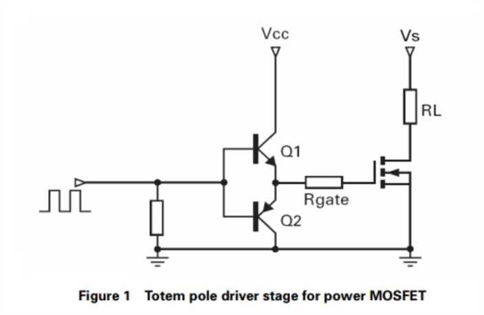
source: DN80 - Bipolar transistors for MOSFET gate driving applications (diodes.com)
Struggling with the Calculations. Feel Free to Skip This!
I struggled with some formulas that stated, that average Gate current during the switching event can be calculated as
IG = Q/t, where:
- IG is the average gate current
- Q is the total gate charge (QGS + QGD)
- t is the switching transient time (ton or toff)
In my case for a switching transient time of 200 ns I needed IG = 25E-9 / 2E-7 = 0.125 A
This is cause the charge necessary to fully enhance a power MOSFET derives from its Gate-Source and Gate-Drain capacitances and is delivered via an external resistor. The Gate voltage follows a characteristic RC time constant which (within EMI constraints) has to be short enough to traverse the linear region without incurring excessive switching losses in the power MOSFET.
Continuing with the calculations to figure out how to adjust the driver with the Arduino output, I arrived at a formula for calculating the power dissipated by the two transistors in the totem-pole setup. It's amusing because in the previous blog, I mentioned that I wasn't going to do calculations and that we would rely on intuition.
The power MOSFET is required to switch at a frequency of 100 kHz and driven to 8VGS the power dissipation in each driver transistor can be calculated, worst case (assuming Rg = 0), as approximately:
Q = 25 nC @ 10 V
PD(npn) = ((VCC- VG/2) • Q • f) + (VBE • IB • t • f) = ((12 - 4) * 25E-9 * 1E5) + (0.8 * 0.8E-3 * 2E-7 * 1E5) = 0.02W
PD(pnp) = ((VG/2) • Q • f) + (VBE • IB • t • f) = ((4 * 25E-9 *1E5) + (0.8 * 0.8E-3 * 2E-7 * 1E5) = 0.01W
where:
- PD is the power dissipation
- VCC is the driver stage supply voltage (assumed in this case to be 12V)
- IG is the average gate current
- t is the switching transient time (ton or toff)
- f is the switching frequency
- VBE(on) is the forward base-emitter voltage
- IB is the transistor base current (Ic/hFE)
Then I arrived at another formula for choosing the value of a bypass capacitance for the totem-pole driver. I did my homework here as well, but I didn't manage to improve the results.
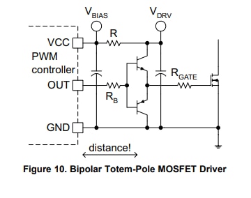 source 3.2 Bipolar Totem-Pole Driver: Fundamentals of MOSFET and IGBT Gate Driver Circuits
Cdrv = (Iqhi * Dmax / fdrv + Qg) / Vripple
where:
- Iqhi is the quiescent current of the driver when its input is driven high
- Dmax is the maximum duty cycle of the driver while the input can stay high
- fdrv is the operating frequency of the driver
- Qg is the total gate charge based on the amplitude of the gate drive and drain-to source off state voltages.
- Vripple
Cdrv = (0.125 * .50 / 100000 + 25E-9) / .1 = 6.5 uF
Applying theoretical calculations and making things worse and then better...
I conducted various tests, implementing the improvements they suggested, but the situation improved marginally or even worsened.
After some uncertainty, I decided to replace the NPN 2N5551 and its complementary PNP 2N5401 transistors with a pair designed for lower currents: the NPN 2N3904 and the PNP 2N3906. Additionally, I introduced a preceding inverting stage to ensure that the Arduino R4 could operate in a safe zone below 8 mA. The GPIOs on the R7FA4M1AB3CFM#AA0 microcontroller can handle currents of up to 8 mA safely.
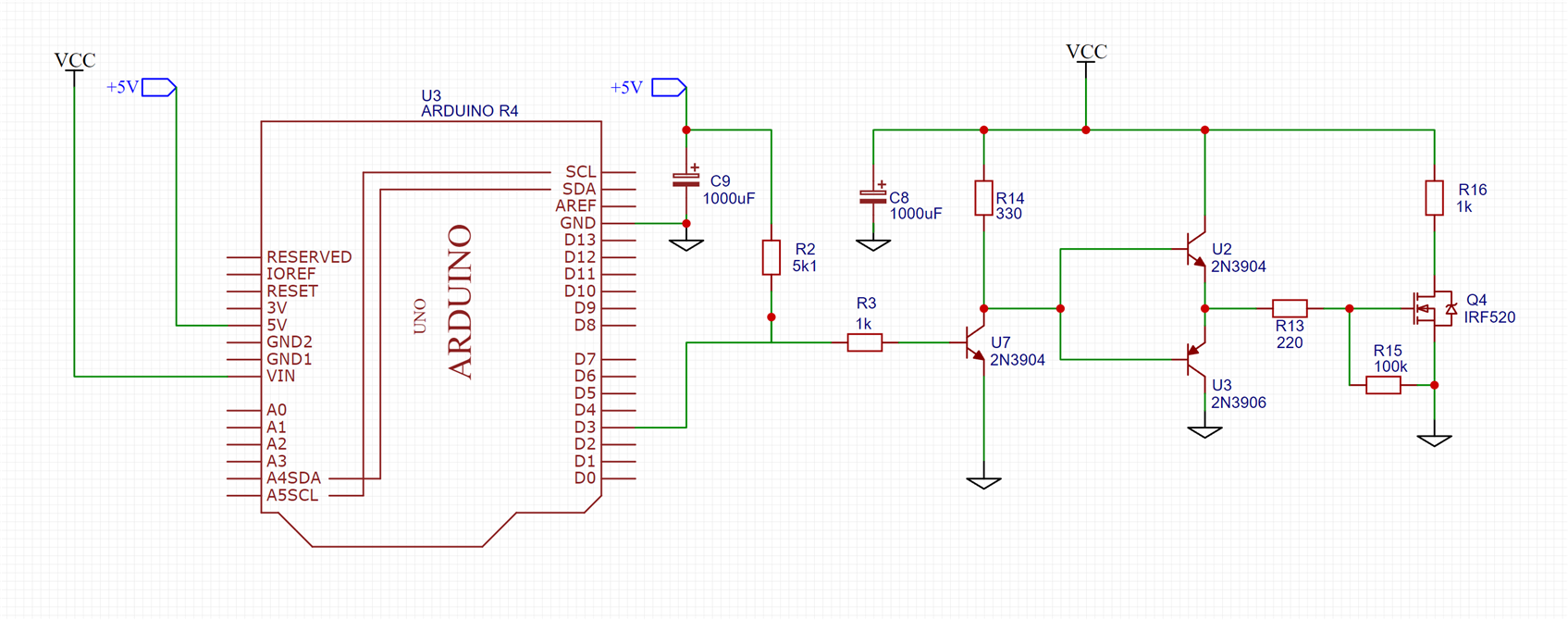
Things improved significantly, but the IRF530 MOSFET still struggled to switch at low duty cycles. I replaced the IRF530 MOSFET with an IRF520 MOSFET, and voila, everything started working better. Several changes to resistor values using the scientific method of trial and error led me to a solution that I found more satisfactory.

Below, you can see three tables that I used for the comparison of the semiconductors I was going to replace:
Comparing the NPN3904 with the NPN5551
| Transistor Type | NPN3904 | NPN5551 |
| Current - Collector (Ic) (Max) | 200 mA | 600 mA |
| Voltage - Collector Emitter Breakdown (Max) | 40 V | 160 V |
| Vce Saturation (Max) @ Ib, Ic | 300mV @ 5mA, 50mA | 200mV @ 5mA, 50mA |
| Current - Collector Cutoff (Max) | - | 50nA (ICBO) |
| DC Current Gain (hFE) (Min) @ Ic, Vce | 100 @ 10mA, 1V | 80 @ 10mA, 5V |
| Power - Max | 625 mW | 625 mW |
| Frequency - Transition | 300MHz | 100MHz |
Comparing the PNP3904 with the PNP5551
| Transistor Type | PNP3906 | PNP5401 |
| Current - Collector (Ic) (Max) | 200 mA | 600 mA |
| Voltage - Collector Emitter Breakdown (Max) | 40 V | 150 V |
| Vce Saturation (Max) @ Ib, Ic | 400mV @ 5mA, 50mA | 500mV @ 5mA, 50mA |
| Current - Collector Cutoff (Max) | - | - |
| DC Current Gain (hFE) (Min) @ Ic, Vce | 100 @ 10mA, 1V | 60 @ 10mA, 5V |
| Power - Max | 625 mW | 625 mW |
| Frequency - Transition | 250MHz | 400MHz |
Change the MOSFET IRF520 by the MOSFET IRF530
| FET Type | N-Channel IRF520 | N-Channel IRF530 |
| Technology | MOSFET (Metal Oxide) | MOSFET (Metal Oxide) |
| Drain to Source Voltage (Vdss) | 100 V | 100 V |
| Current - Continuous Drain (Id) @ 25°C | 9.7A (Tc) | 14A (Tc) |
| Drive Voltage (Max Rds On, Min Rds On) | 10V | 10V |
| Rds On (Max) @ Id, Vgs | 200mOhm @ 5.7A, 10V | 160mOhm @ 8.4A, 10V |
| Vgs(th) (Max) @ Id | 4V @ 250µA | 4V @ 250µA |
| Gate Charge (Qg) (Max) @ Vgs | 25 nC @ 10 V | 26 nC @ 10 V |
| Vgs (Max) | ±20V | ±20V |
| Input Capacitance (Ciss) (Max) @ Vds | 330 pF @ 25 V | 670 pF @ 25 V |
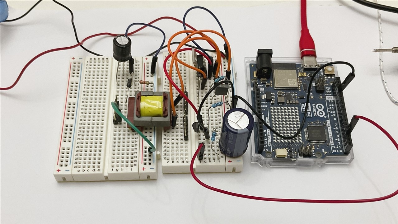
Testing the new driver. Still on a breadboard.
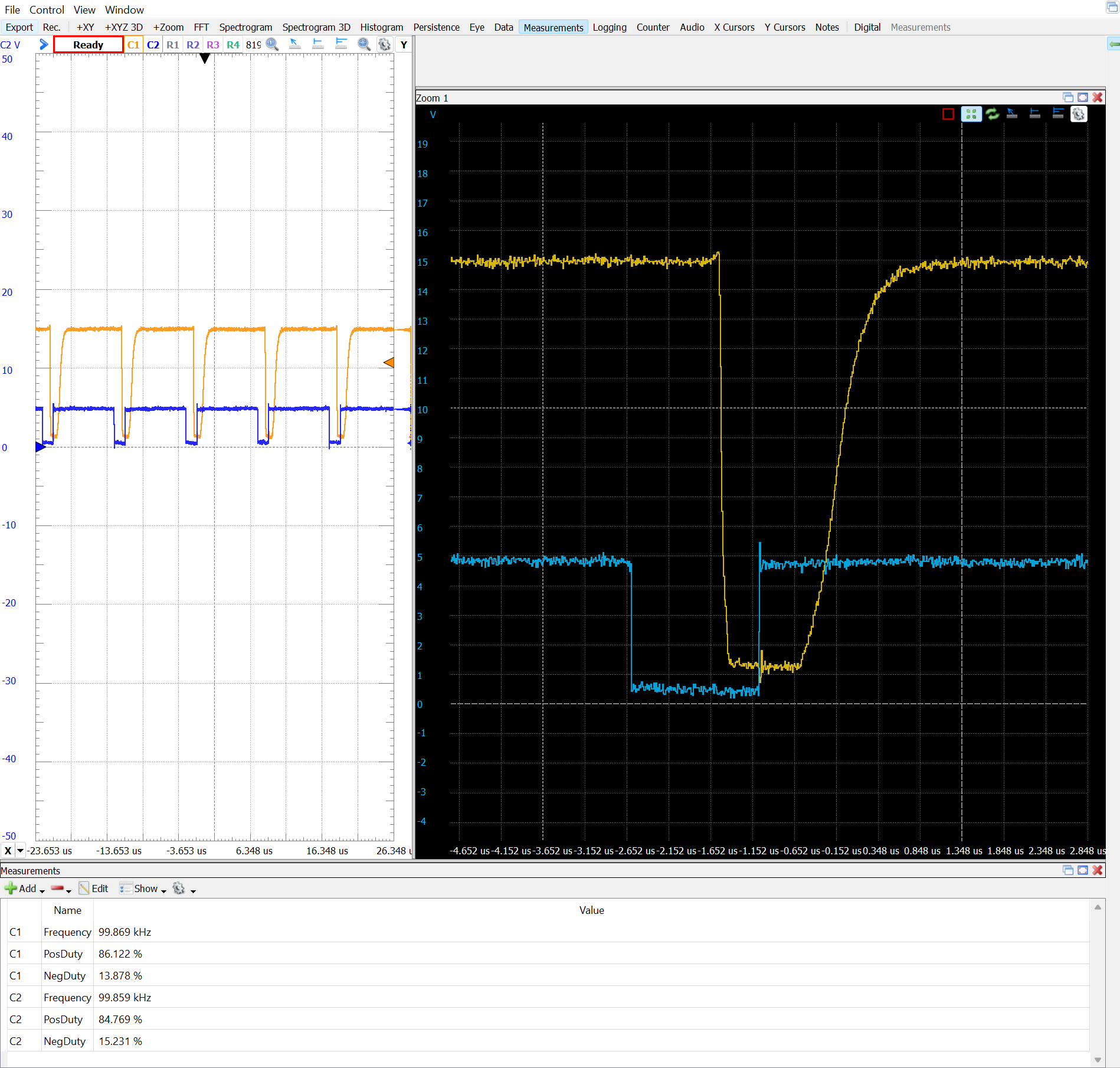
The following images are from my Analog Discovery 2. I'm comparing the PWM signal from the digital output port of the Arduino with the voltage at the drain of the MOSFET. The Arduino's output signal, 15% Duty cycle, is inverted by software so that, after passing through the inverting stage of the first NPN transistor, it returns to the direct orientation.
When the MOSFET is conducting, the voltage at the drain drops to ground.
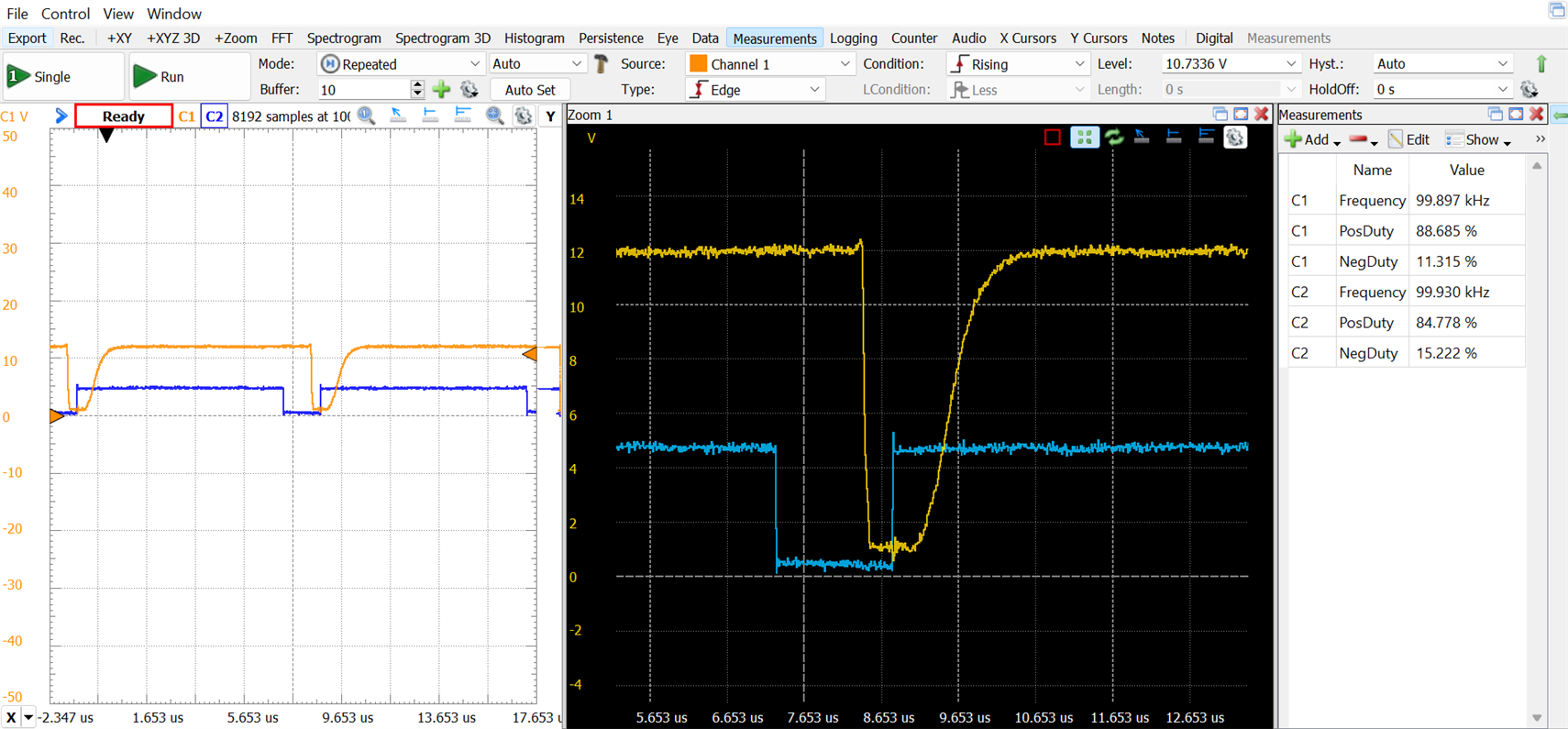
Several more periods:
Developing a soft-start control algorithm for the driver
During startup, the MOSFET undergoes significant stress. To preempt potential issues, I not only adjusted the software driver to invert the signal but also implemented an algorithm known as soft start. This algorithm slowly adjusts the duty cycle of the PWM signal from zero to the target value, mitigating stress on the MOSFET and preventing potential problems.
Here is the code for an Arduino R4.
#include "pwm.h"
#include "math.h"

// PWM PERIOD FOR A 100 kHz frequency, 10 us
#define PWM_PERIOD_USEC 10
// Arduino output port for the PWM signal
#define PWM_SIGNAL_PIN D3
#define PWM_SOFTSTART_TARGET_DUTY_PCTE 15.0
#define PWM_TIME_BETWEEN_TRANSITIONS_MS 10

PwmOut pwm(PWM_SIGNAL_PIN);

/**
* PRE: Given the Duty cycle in percentage 0.0 to 100.0
* for the inverted pwm signal High off, Low on.
* POS: Sets the pwm duty cycle for the inverted
* pwm signal. High off, Low on.
*/
bool invertedPwmPerc(float invert_duty_cycle_pcte) {
  if (invert_duty_cycle_pcte > 100.0) {
    invert_duty_cycle_pcte = 100.0;
  }
  if (invert_duty_cycle_pcte < 0.0) {
    invert_duty_cycle_pcte = 0.0;
  }
  return pwm.pulse_perc(100.0 - invert_duty_cycle_pcte);
}

/**
* PRE: Given the initial duty cycle in percentage 0.0 to 100.0,
* the target duty cycle in percentage 0.0 to 100.0 for the PWM signal
* and the dalay between steps
* POS: Performs a soft transition between the two duty cycles
*/
bool pwmSoftTransition(float initial_duty_cycle, float target_duty_cycle, float time_steps_ms) {
  float pcte_increments;

  if (target_duty_cycle > initial_duty_cycle) {
    pcte_increments = .1;
  } else {
    pcte_increments = -.1;
  }

  int steps_delay = (int)(abs(target_duty_cycle- initial_duty_cycle) / .1);

  float percentage = initial_duty_cycle;
  for (int i = 0; i < steps_delay; ++i) {
    percentage += pcte_increments;
    bool success = invertedPwmPerc(percentage);
    if (!success) {
      return false;
    }
    delay(time_steps_ms);
  }
  return true;

}

/**
* PRE: Given the target duty cycle in percentage 0.0 to 100.0 for the PWM signal
* and the delay between steps in ms
* POST: Performs a soft start till reaching the target duty cycle
*/
bool pwmSoftStart(float target_duty_cycle, float time_steps_ms) {
    return pwmSoftTransition(0.0, target_duty_cycle, time_steps_ms);
}

void setup() {

  pwm.begin(PWM_PERIOD_USEC, 0.0);
  pwmSoftStart(PWM_SOFTSTART_TARGET_DUTY_PCTE, PWM_TIME_BETWEEN_TRANSITIONS_MS);
}


void loop() {

}
And in the next video, you can observe the output at the output D3 port of the Arduino R4.
Applying the Soft-start to the MOSFET
Applying the softstart to the MOSFET
Choosing a new transformer more in line with the requirements
In the previous scenario, I creatively repurposed a flyback transformer designed for mains voltage, experimenting with winding ratios and using various windings individually or in series to achieve lower voltages. In this new exercise, I will opt for the most appropriate transformer available in the kit, the BA60951CS XFMR.Buy Now
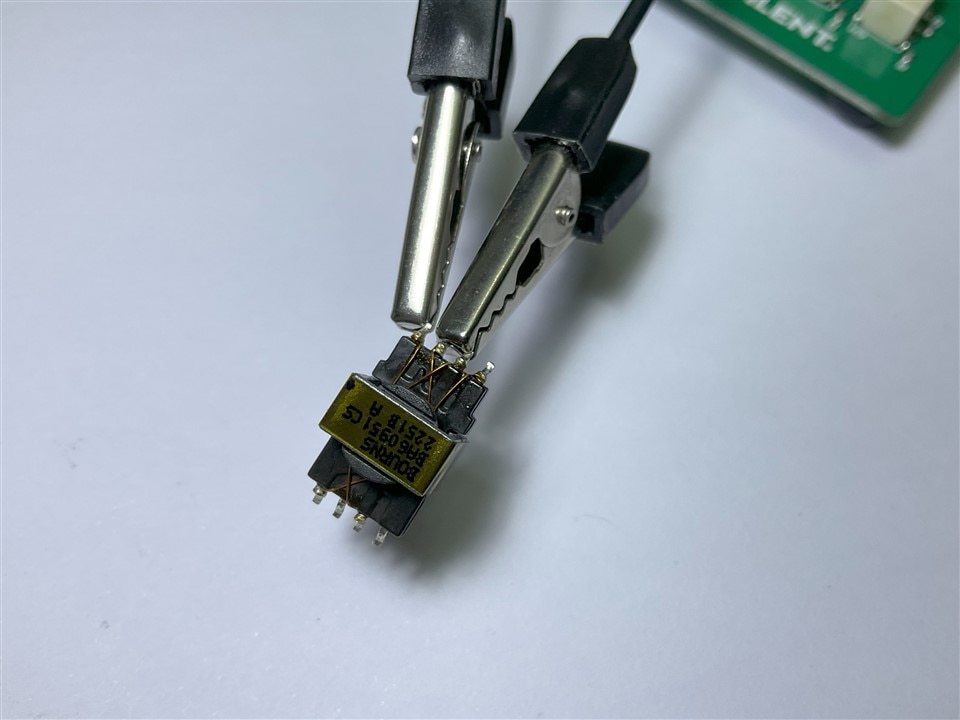
Bourns BA60951CS 2.25W Flyback Transformers are automotive-grade, AEC-Q200-compliant flyback transformers in a low-profile SMT package (2.9mm x 2.4mm x 1.1mm). The BA60951CS is designed for a 250kHz switching frequency and provides 2.25W output power. This transformer can be used with many flyback controller ICs and can be customized for other output voltages and applications.
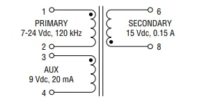
Primary Input Voltage ..................... 7-24 V
Auxiliary Voltage .................... 9 V, 20 mA
Secondary Voltage ............ 15 V, 150 mA
Primary Rated Current.....................1.4 A
Frequency...................................120 kHz
Hi-Pot Prim/Sec ..............2500 Vac / 60 s
It has an auxiliary winding which provides a low-voltage reference for control circuits. The winding may introduce noise caused by common mode current and affect the secondary circuit. A great way to mitigate the issue is to place a small capacitor between the ground of the auxiliary winding and the ground of the load on the secondary winding. I haven't used this auxiliary winding for the current exercise.
Learning more about the BA60951CS transformer. Identifying terminals.
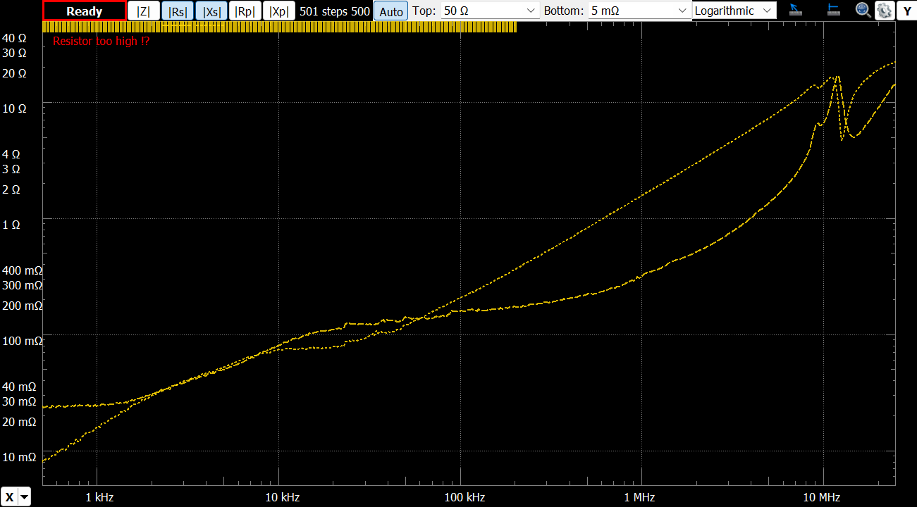
The BA60951CS is a familiar component that I previously explored in the second blog, Examining BA60951CS – Flyback Transformer . At that time, I didn't fully grasp the significance of measuring the leakage inductances of this transformer. Let's quickly revisit them; later, these measurements will aid us in theoretical calculations to determine the values of components required for snubber network circuits and voltage clamps.
Leakage inductance Primary (AUX winding), secondary shorted
Warning: the transformer is not designed to operate this way, this is a learning exercise. The analog discovery 2 has a bandwidth of 20 MHz, results above 10 MHz are meaningless.
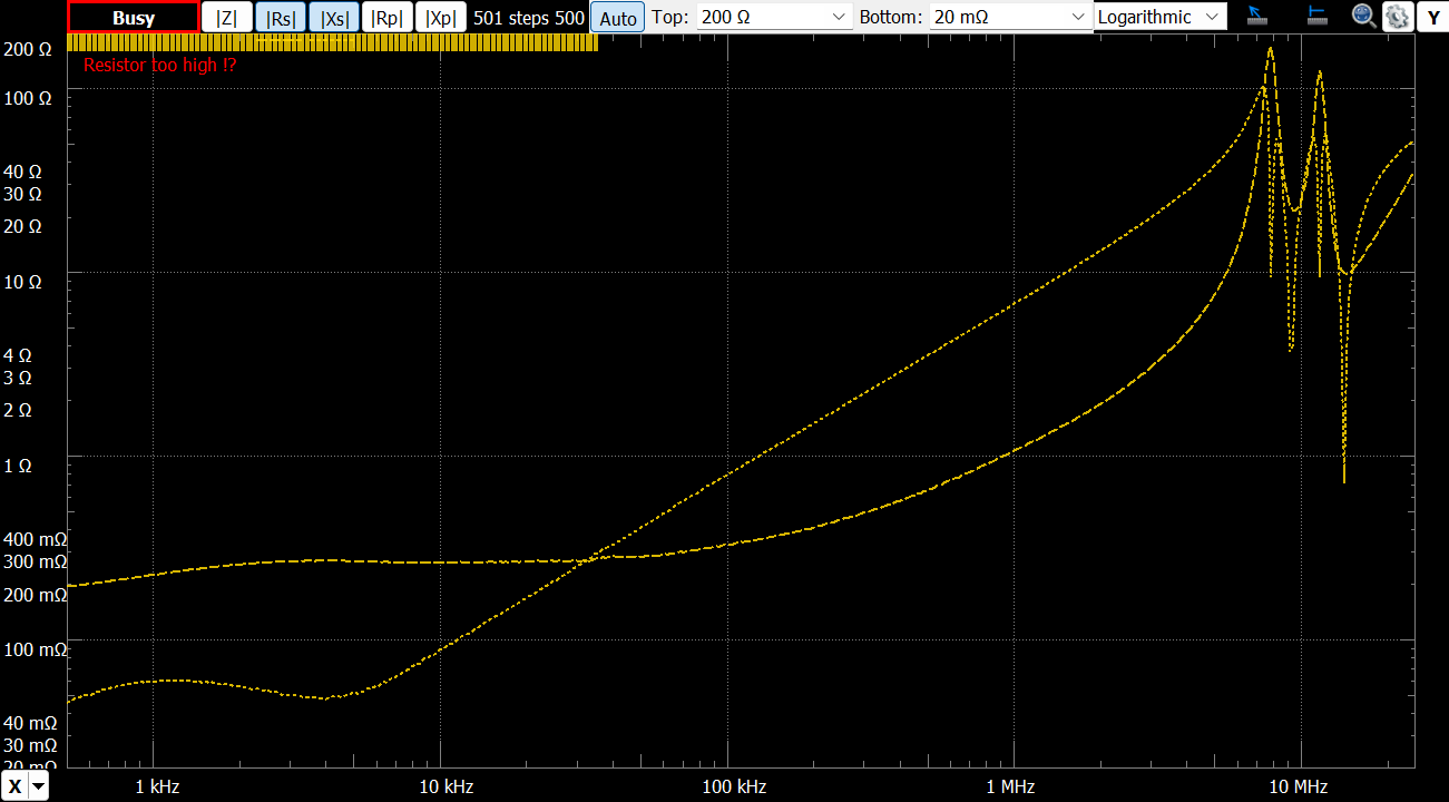
When the MOSFET switches to off there is some high frequency ringing.
For better resolution open-zoom this one
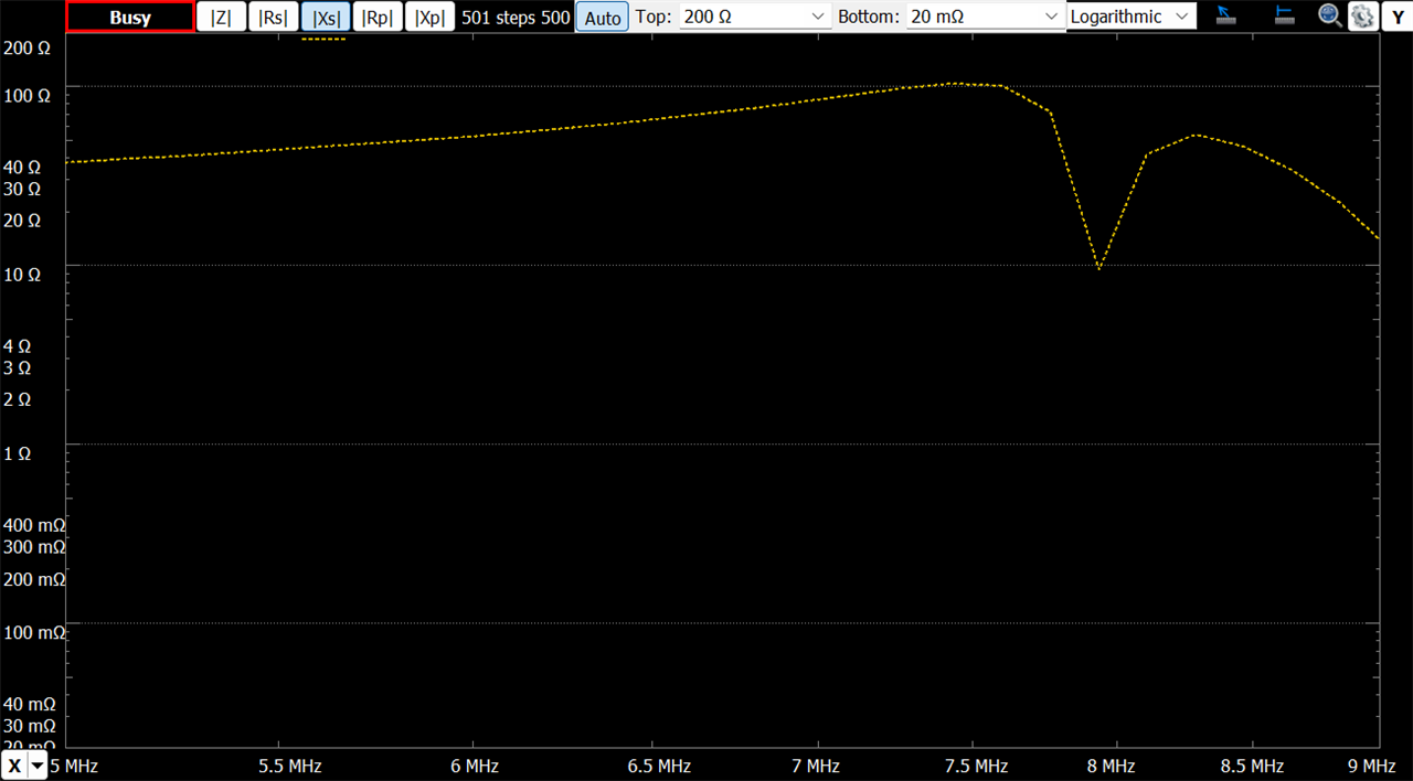
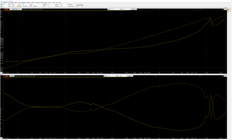
Leakage inductance Secondary, primary (AUX winding) shorted
Warning: the transformer is not designed to operate this way, this is a learning exercise. The Analog Discovery 2 has a max sample rate of 100MS/s (millions of samples per second) we get a maximum of 10MHz sample frequency at 10,000 samples. Results above 10 MHz are meaningless.
For better resolution open-zoom this one
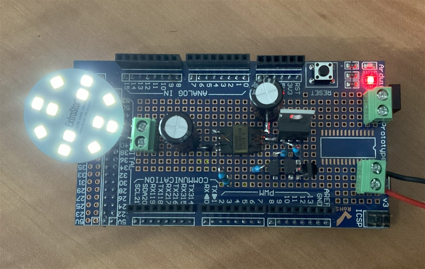
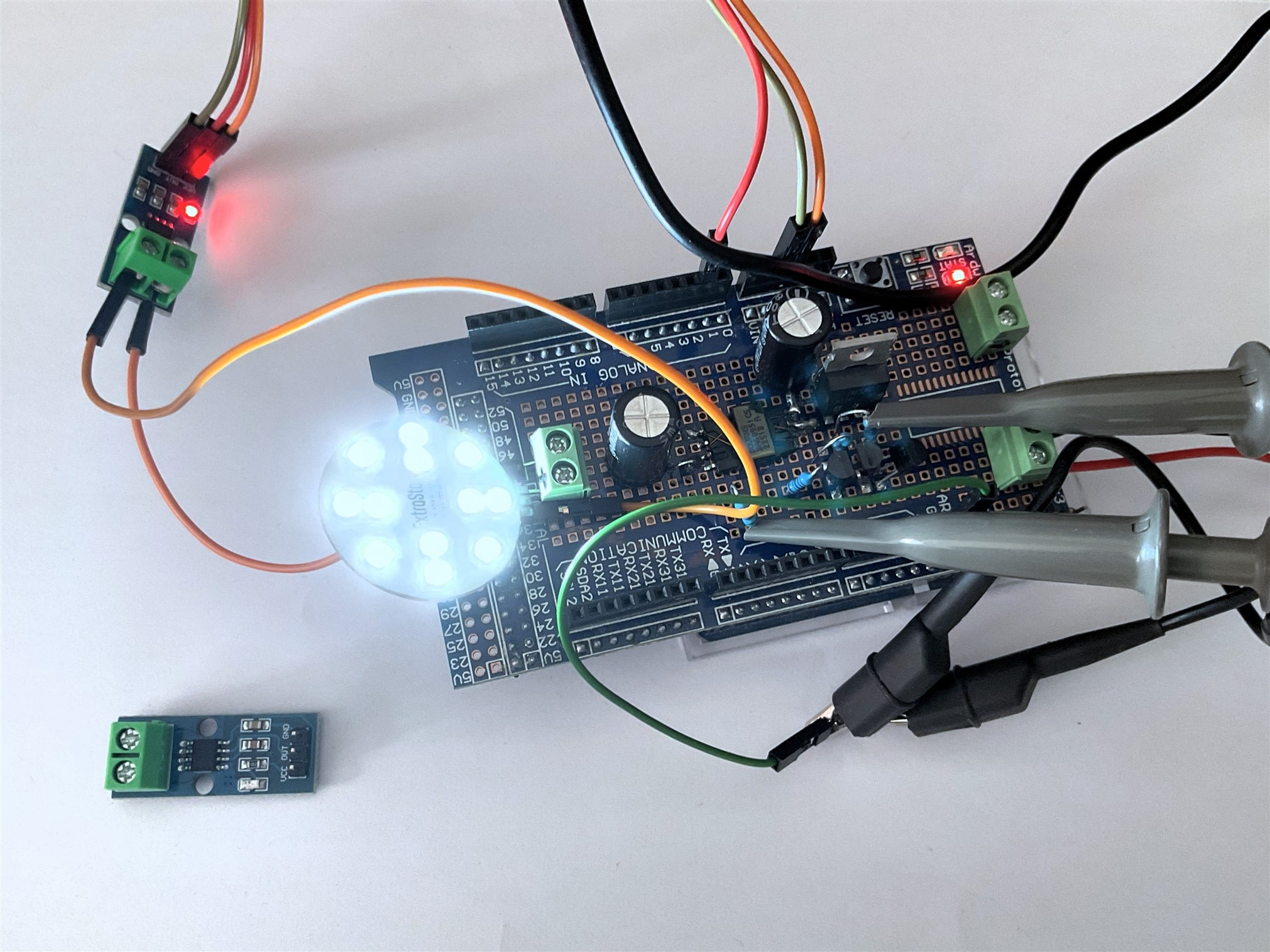
Creating an Arduino shield for our DC/DC converter to drive a LED array
After all the new choices and testing on the protoboard, I proceeded to solder everything onto an Arduino shield board. At this point, I haven't added snubber or voltage clamp circuits to observe the oscillations during MOSFET turn-offs once again.

Hard reset and soft start tests
Pleasantly surprised that everything worked on the first attempt. Below, I present some of the results obtained with the newly constructed Arduino shield board.
In the next video, the system performs two soft starts after an Arduino reset. Two hard resets. Power comes from a 72-8690A TENMA DC Power Supply. It is powering both the Arduino and the converter that acts as the driver for the LED lamp.
Observing oscillations without snubbers and voltage clamps.
Working with soldered components is more enjoyable, and the results are much more promising.
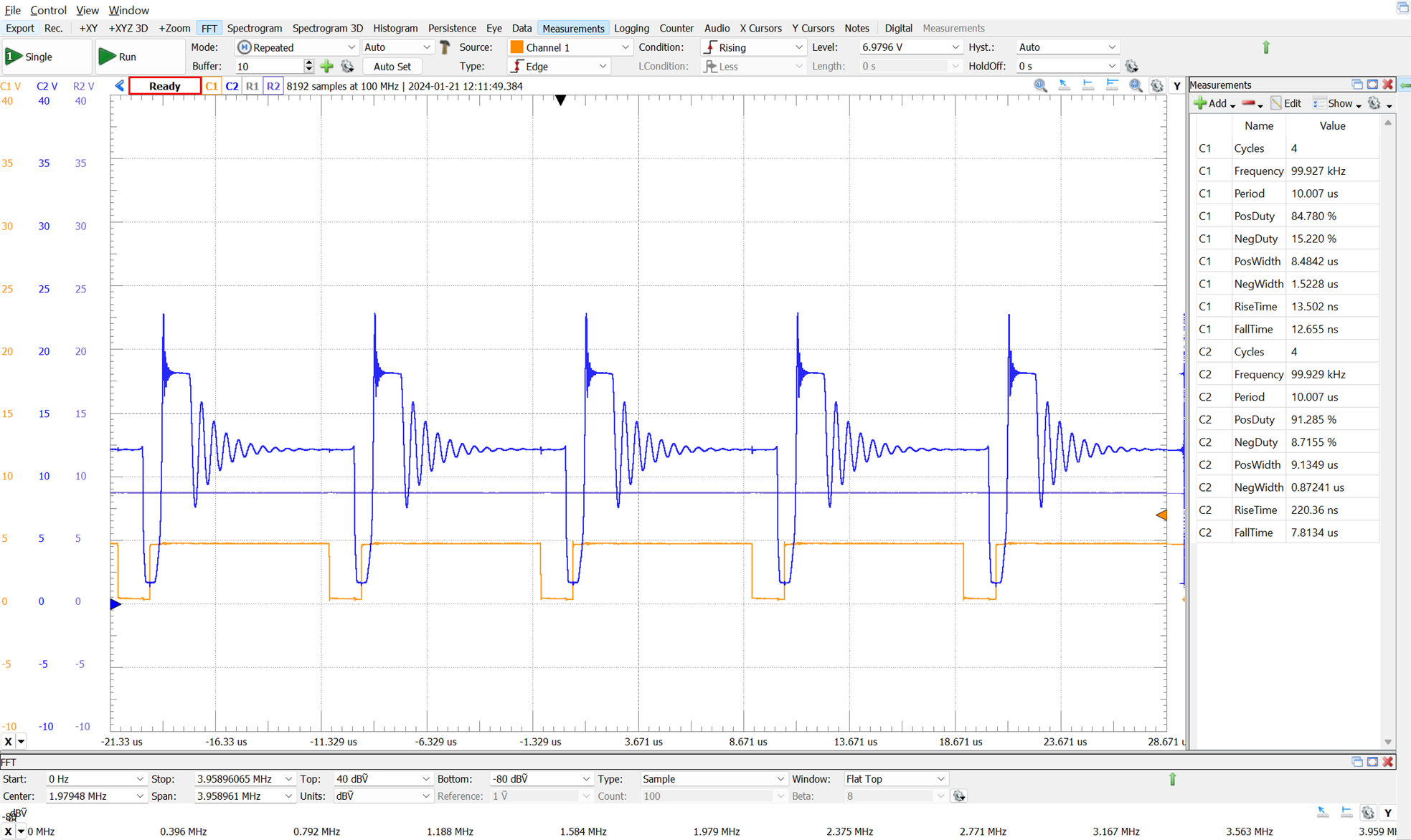
The following image shows the drain-to-source voltage on the MOSFET (Channel C1) against the voltage applied to the MOSFET gate (Channel C2)
V Drain-Source VCC 12V Duty Cycle 15%
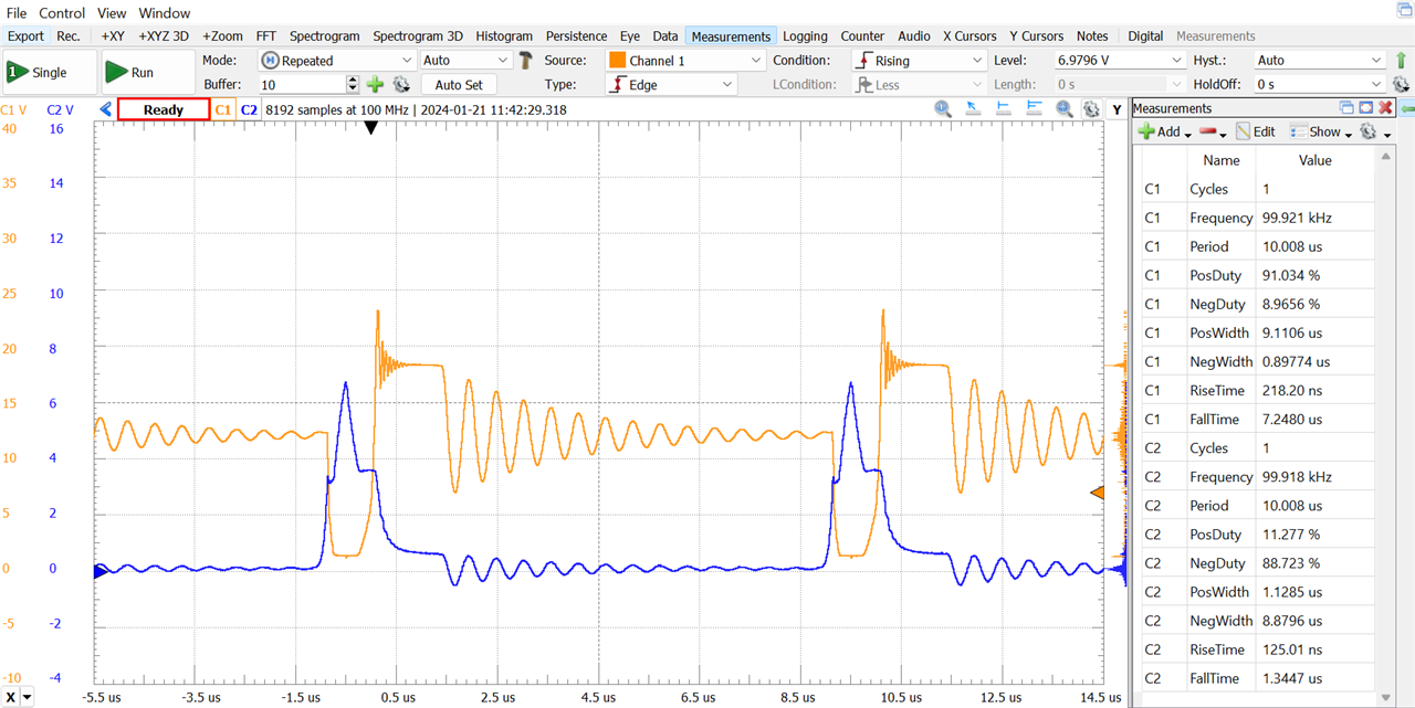
When the switch goes into cutoff, the magnetic field induces a voltage in the secondary, turning the primary winding into a generator. Voltage reverses on both sides, primary and secondary, initiating current flow in the secondary.
The leakage coil is charged and will charge the parasitic capacitor of the switch. The capacitor then releases energy, recharging the "leakage inductor" in the opposite direction until the capacitor is discharged. This process repeats until the oscillations disappear. Similar behavior occurs in the diode during cutoff, causing another oscillation in diode switching.
Same experiment with a 9 V DC input voltage and the same duty cycle. These conditions are similar to those in the previous blog.
V Drain-Source VCC 9V Duty Cycle 15%
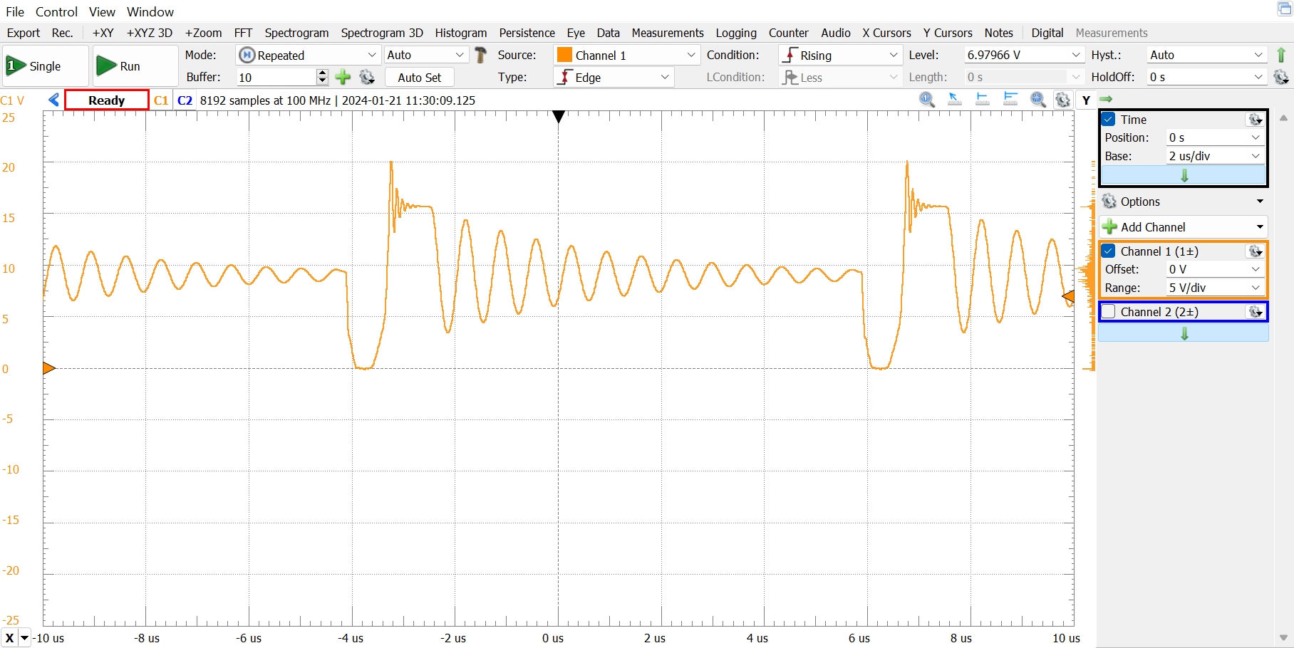
To understand the behavior, we need to take into account the parasitic components.
source: Design Guidelines for RCD Snubber of Flyback Converters
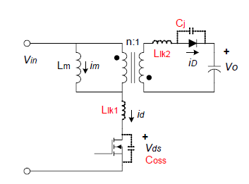
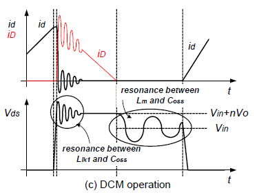
When the MOSFET turns off, a high-voltage spike occurs on the drain pin because of a resonance between the leakage inductor (Llk) of the main transformer and the output capacitor (COSS) of the MOSFET. When the main switch turns on, the energy is stored in the transformer as a flux form and is transferred to output during the main switch off-time.
The converter is operating in discontinuous mode (DCM), the secondary current runs dry before the end of one switching period.
There is a resonance between Lm and the output capacitor COSS of the MOSFET. When the MOSFET turns off, the primary current (id) charges COSS of the MOSFET in a short time.
When the voltage across COSS (Vds) exceeds the input voltage plus reflected output voltage (Vin+nVo), the secondary diode turns on, so that the voltage across the magnetizing inductor (Lm) is clamped to nVo. There is, therefore, a resonance between Llk1 and COSS with high-frequency and high-voltage
surge.
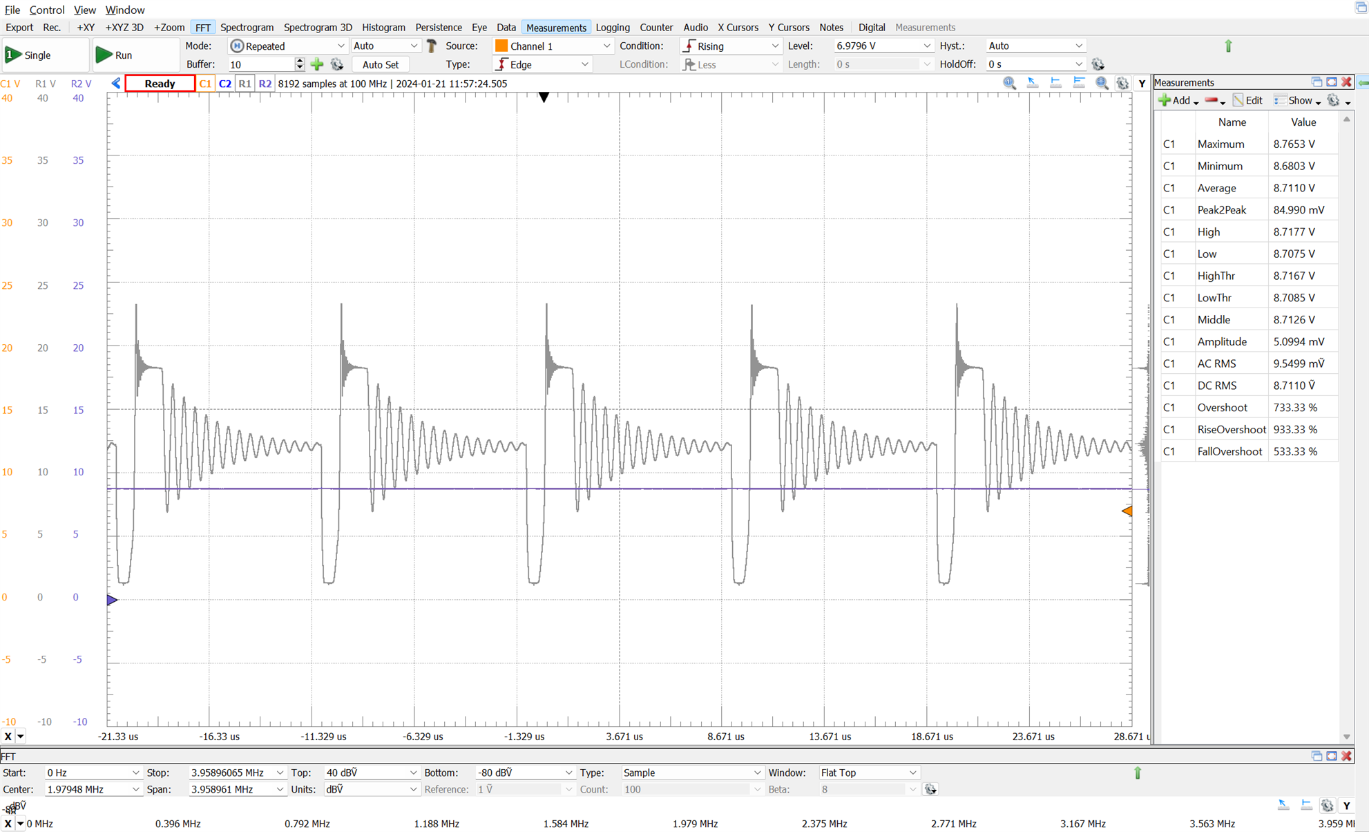
Output Voltage
The image below illustrates the drain voltage, the Arduino's PWM signal, and the relatively straight line represents the converter's output voltage. This is a significant improvement compared to the previous blog, where there was more noticeable ripple in the output.
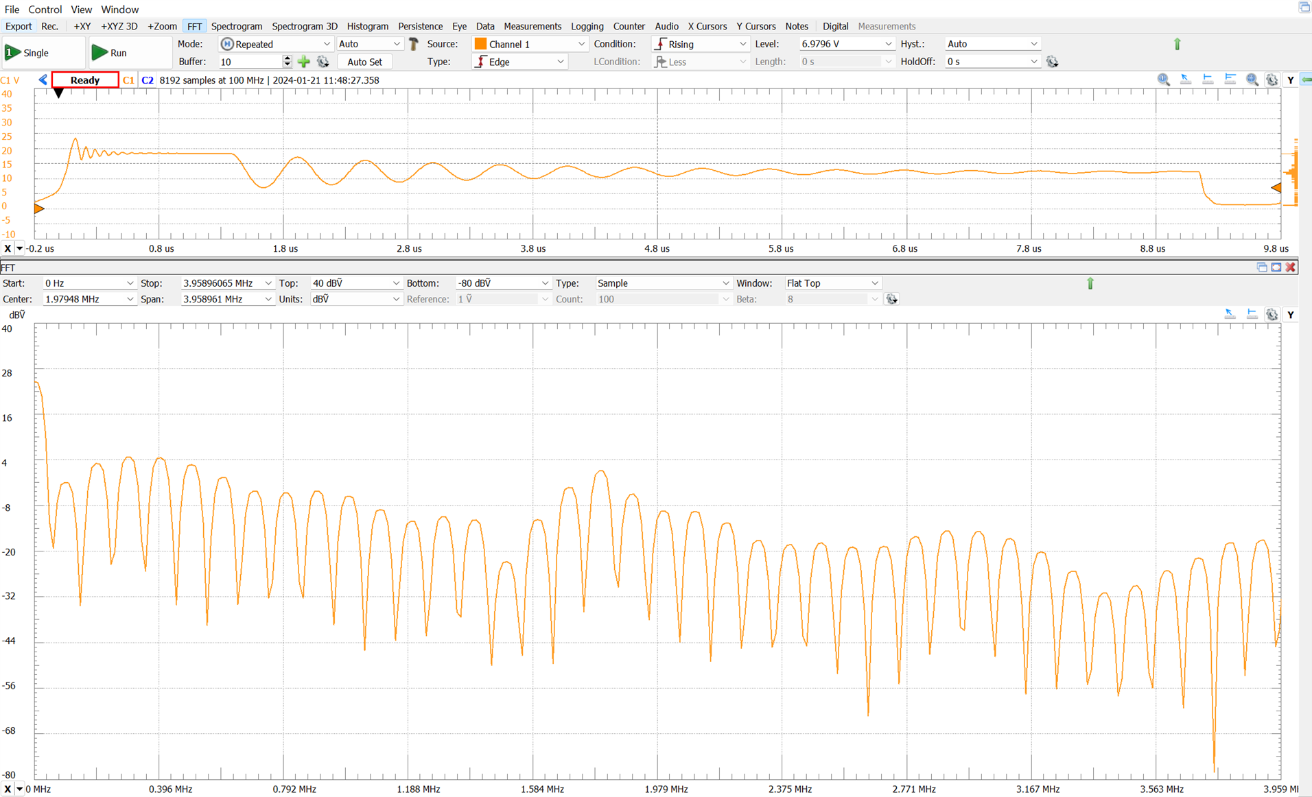
Frequency analysis of ringing during switching.
V Drain-Source VCC 12V Duty Cycle 15% FFT
We can observe peaks at certain frequencies caused by various oscillations.
Output signal without snubber circuits.
V Drain-Source VCC 12V Duty Cycle 15% FFT
Vout 8.71 VCC
A 200-lumen/148 mA LED lamp, is connected as the load.
Regulation Feedback
Until now I have worked on a converter without any regulation. There are several methods to carry out the regulation as explained in the previous blog, see:Regulation in flyback converters section.
In this exercise I have attempted to take a different approach to that regulation. The regulation is carried out from an Arduino microcontroller by software and the feedback loop is carried out by taking measurements using a current probe that uses a hall effect sensor with little effect on the circuit.
The Arduino Uno R4 boards are based on the Renesas RA4M1 ARM Cortex M4 CPU, with 256 KB flash memory, 32 KB RAM, and a 48 MHz clock. They have an Analog-to-Digital Converter (ADC) that transforms an analog signal to a digital one supporting up to 14-bit resolutions.
To update the resolution, you only need to use the analogReadResolution() command. To use it, simply include it in your setup(), and use analogRead() to retrieve a value from an analog pin.
void setup(){
  analogReadResolution(14); //change to 14-bit resolution
}

void loop(){
  int reading = analogRead(A3); // returns a value between 0-16383
}
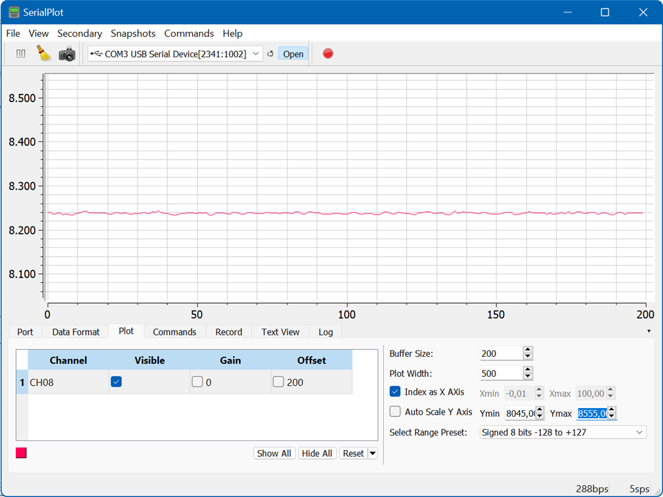
The current sensor on the output.is an ACS172 module (ACS712: Hall-Effect-Based Linear Current Sensor IC ) , a fully Integrated, Hall effect-based linear current sensor.
Arduino code for the next tests on the current sensor readings:
#include "pwm.h"
#include "math.h"

// PWM PERIOD FOR A 100 kHz frequency, 10 us
#define PWM_PERIOD_USEC 10
// Arduino output port for the PWM signal
#define PWM_SIGNAL_PIN D3
#define PWM_SOFTSTART_TARGET_DUTY_PCTE 15.0
#define PWM_TIME_BETWEEN_TRANSITIONS_MS 10

const int analogInPin = A1;  // Analog input pin that the current sensor is attached to
float sensorValue = 0.0;  // value read from the pot


PwmOut pwm(PWM_SIGNAL_PIN);

/**
* PRE: Given the Duty cycle in percentage 0.0 to 100.0
* for the inverted pwm signal High off, Low on.
* POS: Sets the pwm duty cycle for the inverted
* pwm signal. High off, Low on.
*/
bool invertedPwmPerc(float invert_duty_cycle_pcte) {
  if (invert_duty_cycle_pcte > 100.0) {
    invert_duty_cycle_pcte = 100.0;
  }
  if (invert_duty_cycle_pcte < 0.0) {
    invert_duty_cycle_pcte = 0.0;
  }
  return pwm.pulse_perc(100.0 - invert_duty_cycle_pcte);
}

/**
* PRE: Given the initial duty cycle in percentage 0.0 to 100.0,
* the target duty cycle in percentage 0.0 to 100.0 for the PWM signal
* and the dalay between steps
* POS: Performs a soft transition between the two duty cycles
*/
bool pwmSoftTransition(float initial_duty_cycle, float target_duty_cycle, float time_steps_ms) {
  float pcte_increments;

  if (target_duty_cycle > initial_duty_cycle) {
    pcte_increments = .1;
  } else {
    pcte_increments = -.1;
  }

  int steps_delay = (int)(abs(target_duty_cycle- initial_duty_cycle) / .1);

  float percentage = initial_duty_cycle;
  for (int i = 0; i < steps_delay; ++i) {
    percentage += pcte_increments;
    bool success = invertedPwmPerc(percentage);
    if (!success) {
      return false;
    }
    delay(time_steps_ms);
  }
  return true;

}

/**
* PRE: Given the target duty cycle in percentage 0.0 to 100.0 for the PWM signal
* and the delay between steps in ms
* POST: Performs a soft start till reaching the target duty cycle
*/
bool pwmSoftStart(float target_duty_cycle, float time_steps_ms) {
    return pwmSoftTransition(0.0, target_duty_cycle, time_steps_ms);
}

void setup() {
    // initialize serial communications at 9600 bps:
  Serial.begin(9600);
  analogReadResolution(14); //change to 14-bit resolution

  pwm.begin(PWM_PERIOD_USEC, 0.0);
  pwmSoftStart(PWM_SOFTSTART_TARGET_DUTY_PCTE, PWM_TIME_BETWEEN_TRANSITIONS_MS);
}


void loop() {
    // read the analog in value:
  float sensorValueOld = sensorValue;
  sensorValue = 0.0;
  for (int i = 0; i < 100; i++) {
     sensorValue += analogRead(analogInPin);
    // wait 2 milliseconds before the next loop for the analog-to-digital
    // converter to settle after the last reading:
     delay(2);
  }
  sensorValue =  (sensorValue / 100.0 + sensorValueOld) / 2.0;
  Serial.println(sensorValue);


}
This is the captured data after applying a low pass-filter. Values ranging from 0 to 16384 with 8192 corresponding to 0A
The need for snubber circuits and voltage clamps
In the previous blog, Flyback converter with primary snubber, we saw the beneficial effects of using a snubber circuit and a voltage clamp to reduce oscillations. Given the results obtained in this blog without protections, let's delve into the topic again.
Semiconductors have strict limits on maximum voltage, current, and power values. Exceeding these limits could lead to device destruction. Components like snubbers or voltage clamps, are crucial in many power circuits.
Their role is to reduce stress on semiconductor devices during switching, addressing issues like overvoltage and high power losses, ensuring safe operation. Snubber circuits absorb energy from the circuit's capacitance and inductance during switching, controlling voltage and/or current in the semiconductor switch. This enhances semiconductor reliability by minimizing degradation from increased power dissipation and internal temperature.
For instance, if the internal temperature of a MOSFET doubles, the conduction resistance between drain and source may increase by 50%, leading to increased conduction losses and semiconductor deterioration.
During the transition from conduction to cutoff, oscillations occur due to parasitic capacitances of semiconductors, including the drain-source capacitance and the diode anode to cathode capacitance.
When using a pulse transformer, there are leaking inductances in both the primary and secondary windings. The transformer, typically with a ferrite core, stores energy as an electromagnetic field. Some of the magnetic flux disperses into the air, creating a dispersion flux. This is considered a loss and can be represented as a series-connected coil with the primary winding. The secondary winding experiences a similar phenomenon.
How do these oscillations, potentially reaching hundreds of volts, occur despite working with low voltage values? When the MOSFET is conducting, a positive voltage is applied to the gate. The parasitic capacitance is nearly discharged because the potential difference between drain and source is small. During this period, energy is stored in the primary winding and the core. Leakage inductance is also charging, representing unused energy stored in the core.
When the switch goes into cutoff, the magnetic field induces a voltage in the secondary, turning the primary winding into a generator. Voltage reverses on both sides, primary and secondary, initiating current flow in the secondary. The leakage coil is charged and will charge the parasitic capacitor of the switch. The capacitor then releases energy, recharging the "leakage inductor" in the opposite direction until the capacitor is discharged. This process repeats until the oscillations disappear. Similar behavior occurs in the diode during cutoff, causing another oscillation in diode switching.
Summary: "I see the light"
Working with components soldered to a printed circuit board dramatically reduces parasitic components and the results are easier to interpret.
I am very happy with the results and, yes, I see the light
I have applied the lessons learned from past experiments and there is less time left to complete the control of the Magic Lightbox.
Magic Lightbox Blog Series
- Blog 1 - Magic Lightbox: Smart LED Dimmer Flyback Driver Project Introduction.
- Blog 2 - Magic Lightbox: Understanding Flyback Transformers. How to characterize them.
- Blog 3 - Magic Lightbox: Understanding Flyback Converters.
- Blog 4 - Magic Light Box: DC/DC Flyback Converter Testbench and LED Dimmer Driver
- Blog 5 - Magic Light Box: Building The Prototype
- Final - Magic Lightbox: Project Summary
-

shabaz
-
Cancel
-
Vote Up
0
Vote Down
-
-
Sign in to reply
-
More
-
Cancel
-

javagoza
in reply to shabaz
-
Cancel
-
Vote Up
0
Vote Down
-
-
Sign in to reply
-
More
-
Cancel
Comment-

javagoza
in reply to shabaz
-
Cancel
-
Vote Up
0
Vote Down
-
-
Sign in to reply
-
More
-
Cancel
Children