


1. Minized Synth I Introduction
|
|
In a music studio, a newbie synth designer is given a complex sound synthesizer and told to bring out the sound of a 'Grand Piano' using subtractive synthesis. After some tweaking, all that's left is a basic sine wave. The senior sound engineer asks, "Is it done?" The newbie grins and says, "Don't worry, if the 'Grand Piano' is in there, I'll bring it out with subtractive synthesis!" Image generated with comicsmaker.ai |

The joke is my adaptation of a joke in Spanish in which a cabinetmaker's apprentice is commissioned to try to extract a "San José" from a piece of wood and when he barely has a splinter left he exclaims that if the "San José" is inside from the billet of wood it will come out at any moment. Subtractive synthesis is about, sculpting a sound starting from a sound full of harmonics through filtering and envelopes.
One of the primary forms of synthesis is subtractive synthesis. This technique involves removing undesirable frequencies to create the desired sound. It operates under the assumption that a basic oscillator can produce waveforms with varying frequency spectrums that mimic the sound of an acoustic instrument. The signal then passes through a filter that compensates for the frequency-dependent losses and resonances in the body of the instrument. The amplifier section of the synthesizer shapes the filtered (or unfiltered) signal over time.

MiniZed Synth I
As part of my "Path to Programmable III Program" final project, I selected DSP from the Core Technology Path. My project involved creating a digital version of a classic analog synthesizer from the 1960s, which utilized the AVNET MiniZed development board. This board is powered by an AMD Zynq 7Z007S single-core development board, which contains an "All Programmable System-On-Chip" (APSoC) that integrates most computer components into one chip. Additionally, it includes FPGA technology that can be utilized.
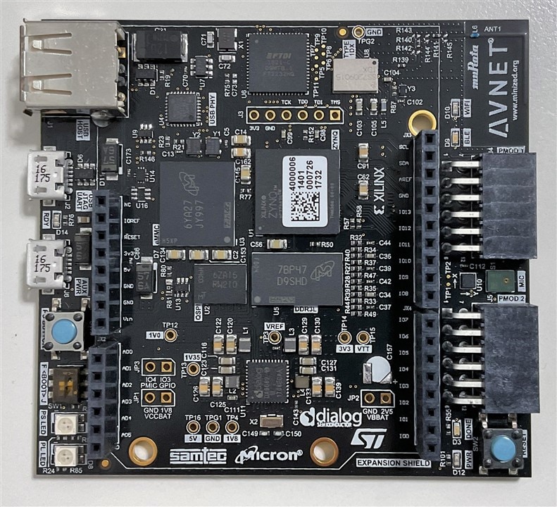
AVNET MiniZed Development Board. The AMD Zynq 7Z007S (Formerly Xilinx Zynq) chip is in the center with the sticker on it.
During the project, several extension boards to the MiniZed board have been designed and built:
- A sound editing panel with 17 analog potentiometers,
- a board with an external analog multiplexer from 2 to 16 channels,
- an extension board with user buttons and indicator LEDs.
- a low-pass filter board for digital-to-analog conversion with an analog audio amplifier
- and a MIDI interface board, this last is designed but not yet built pending receipt of PCBs.
The majority of the work on this project was accomplished using SystemVerilog, a language for describing and verifying hardware used in the creation, design, simulation, testing, and implementation of electronic systems. The MiniZed development board features an AMD Zynq chip, which includes both a microcontroller and a network of Field Programmable Gate Arrays (FPGAs). These FPGAs are semiconductor devices made up of configurable logic blocks (CLBs) that are connected through programmable interconnects. As a result, FPGAs can be reprogrammed after manufacturing to meet specific application or functionality needs. AMD provides a development tool called VIVADO ML that allows the hardware description language to be translated into an interconnect configuration file for the FPGA fabric.
Throughout the past five blog posts, I have been documenting the necessary research and learning required for the successful completion of this project. The blogs covered various aspects such as hardware and software development flow, interfaces and ports of the AVNET Minized development board, and the development of IP blocks in Zynq's FPGA fabric programmable logic for the Vivado development tool. These IP blocks are like Lego pieces that allow bundling and reuse, and there was also a focus on the use of digital filters and hardware-accelerated conversion between Pulse Coded Modulation and Pulse Density Modulation formats. One of the blogs was dedicated to designing an external multiplexer for the Zynq XADC Analog Digital Converter, which is now also a part of the Minized Synth I. At the end of this blog post, you can find references to all the previous posts.
2. Index
Table of Contents
- 1. Minized Synth I Introduction
- 2. Index
- 3. Minized Synth I: Overview and Features
- 4. High-Level Design
- 5. Hardware Accelerated Synth Module IP
- 5.1. Custom Synth Module AXI4 Lite Peripheral IP
- 5.2. What's under the hood of the Synth module?
- 5.3. Oscillators
- 5.4. Sine Wave Generator
- 5.5. Noise Generator Module
- 5.6. Square Wave Generator
- 5.7. Triangle Wave Generator
- 5.8. Saw-Tooth Wave Generator Module
- 5.9. Attack-Decay-Sustain-Release (ADSR) Envelope Modulation
- 5.10. One-bit delta-sigma DAC
- 5.11. Mixer Module
- 5.12. Filter Module
- 5.13. Amplifier Module
- 5.14 Low Frequency Oscillator. Pitch Frequency Modulation
- 6. Minized Microphone Input PDM to PCM via Decimation
- 7. Indicator LEDs and Control Switches Auxiliary Expansion Board
- 8. Low Pass Filter and Sound Amplifier Expansion Boards
- 9. Multiplexer Expansion Board
- 10. ARM 9 Bare Metal Software App. MIDI Control
- 11. Creating the prototype
- 12. Code Repository and References
- 13. Conclusion and next steps
- 14. Path to Programmable III Training Blog Series
3. Minized Synth I: Overview and Features
The MiniZed Synth I is a Monophonic Digital Synthesizer. It features 2 digitally controlled oscillators, a pseudo-random noise generator, a microphone input, a low pass filter, 2 envelope generators, a mixer, and a modulation circuit. The MiniZed Synth has a classic one-knob-per-function design.
Although this first version is monophonic, thanks to the versatility of FPGAs the design can become polyphonic with very little effort by replicating the monophonic module of the synthesizer and creating a dispatcher that assigns the different voices and a new voice mixer module.
FRONT PANEL

MiniZed Synth I Front Panel. It has seventeen analog knobs, four-mode selection pushbuttons, and five-mode or action indicator LEDs.
OSCILLATORS
Two Digital Controlled Oscillators with selectable Sawtooth and Square waveshapes.
NOISE GENERATOR
Shapeable Pseudo Random Noise Generator.
MIC Input
The signal picked up by the MiniZed's microphone can be used as an alternate sound source.
MIX
Mixer for adjusting signal levels independently.
FILTER
12 dB/Octave Digital Low Pass Filter with Adjustable Resonance.
ENVELOPES
Two Attack-Decay-Sustain-Release (ADSR) envelope generators for modulating the filter and amplifier.
The Envelope Decay and Release segments are controlled by the DECAY knob, while the Release segments are enabled or disabled via the RELEASE switch
MOD
MIDI-syncable Low Frequency Oscillator (LFO) with Rate and individual control for the oscillators LFO amount and the filter LFO amount.
AUDIO OUT
1/8" Headphone Output
MIDI
DIN MIDI and USB UART/MIDI bridge
3.1. Signal Flow
The below diagram shows how the MiniZed Synth generates sound. It shows the flow of Audio, Digital Control, and Modulation signals in the MiniZed Synth. Heavy lines indicate 16-bit Pulse Code Modulation (PCM) audio signals flowing from left to right. Lighter lines indicate Digital Control Signals which flow from the bottom. Dotted lines indicate Modulation routings. Spaced-dotted lines indicate 1-bit Pulse Density Modulation (PDM) digital signals

MiniZed Synth Signal Flow Diagram. The diagram shows the different signals used by the synthesizer: control lines, PCM and PDM digital audio signal lines, the modulation routing of the signals, and the final analog sound signal.
The MiniZed Synth's source signals are created by two direct digital frequency synthesis oscillators and a digital Pseudo-Random Noise Generator which are mixed with the MiniZed built-in microphone 1-bit Pulse Density Modulation (PDM) signal previously converted to 16-bit Pulse Coded Modulation (PCM) via decimation.
The Mixer Output is routed to the Filter, where the tone is sculpted according to the Filter parameters and the Filter Attack-Decay-Sustain-Release (ADSR) Envelope.
The signal is then passed to the amplifier stage, where the Volume ADSR envelope shapes it. The Attack-Decay-Sustain-Release (ADSR) envelope modulation scheme is based on the observation that when a real instrument generates a note, the volume of the musical note changes over time. It rises rapidly from zero and then steadily decays.
Finally, the PCM signal is routed to the 1-bit Delta Sigma Digital to Analog Converter and routed to an RC Low Pass Filter. The final level is set by the Analog Volume Control Knob.
Each time the MiniZed Synth receives a MIDI "Note On" command, it produces a Pitch control signal and Gate signal in response. The Pitch control signal sets the Pitch of the Oscillators, while the Gate signal triggers the Filter and Volume ADSR envelopes.
3.2. Basic Operation
The MiniZed Synth I responds to MIDI messages. In addition, Minized Synth has an LED MIDI indicator that indicates MIDI activity on either the DIN MIDI or the USB / UART connector. Additional parameters can be accessed via MIDI control.
3.3. The components
Oscillators
The Oscillators together with the Pseudo-Random Noise Generator are the main source of the MiniZed Synth. They use Direct digital synthesis (DDS) a method employed for creating arbitrary waveforms from a single, fixed-frequency reference that can be tuned and amplified into sound that we can hear. The Mnized Synth can produce a total musical range of 8 octaves.
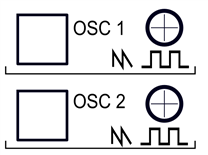
The OSCILLATOR 1 serves as a master Oscillator to which OSCILLATOR 2 is tuned. Two independent switches select the waveform for each Oscillator (Sawtooth or Square). The MiniZed is not limited to these two waveforms but it can also be programmed to generate sinusoidal, triangle, and PWM square waves.
Panel controls for the Oscillators
OSCILLATOR 1 Switch (CC# 70):
Selects a Sawtooth (LED OFF) or Square wave (LED ON) for OSC 1.
OSCILLATOR 2 Switch (CC# 71):
Selects a Sawtooth (LED OFF) or Square wave (LED ON) for OSC 2.
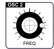
VCO 2 FREQ (CC# 17):
Sets the frequency offset of OSC 2 from OSC 1.
The offset range is +/-1 octave.
Center position tunes OSC 2 in unison with OSC 1.
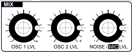
Mixer (Source Levels)
![]()
Each Oscillator (OSC1 & OSC2) has a dedicated level knob that allows you to control the relative strength of each oscillator from 0 to 100%. Another knob allows you to control the relative strength of the other two sound sources, the pseudo-random noise generator, and the MiniZed's internal microphone. A switch selects the third sound source (Mic or Noise). The signal begins to clip the filter at about 2 o’clock creating more aggressive sounds.
Panel Controls for the Mixer
OSC1 LVL (CC# 15):
Sets the level of OSC 1.
OSC 2 LVL (CC# 16):
Sets the level of OSC 2.
NOISE / MIC LVL (CC# 17 / CC# 18)
Sets the level of NOISE or MIC.
Filter
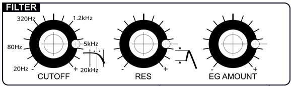
The FILTER is a 12dB/Octave Low Pass Filter design with resonance. It has controls for CUTOFF frequency which determines the range of frequencies the filter will affect, as well as RESONANCE, which determines how much emphasis is applied to the harmonics near the Cutoff frequency.

Frequency response of a Low Pass Filter with Resonance
The FILTER provides either fixed or dynamic timbre modifications. Dynamic changes are provided by the Filter Envelope Generator (EG) and a Low Frequency Oscillator (LFO).
Panel Controls for the Filter
CUTOFF (CC# 19):
Adjusts the CUTOFF frequency of the Low Pass Filter from 20 Hz to 20 KHz. As the knob is rotated clockwise, the cutoff frequency is increased, allowing more harmonics to pass through the filter, resulting in a brighter sound. Conversely, as the knob is rotated counterclockwise, the sounds get darker.
RESONANCE (RES) (CC# 21):
Sets the amount of signal sent from the FILTER output to be fed back into its input. This creates a peak in the frequency that can be increased to self-oscillation.
EG AMOUNT (CC# 22):
Determines how much the Filter Envelope Generator (EG) adds to or subtracts from the Filter Cutoff control setting.
When the EG AMOUNT knob is set to positive (+), turn the FILTER CUTOFF knob left to hear the effect.
When the EG AMOUNT knob is set to negative (-), turn the FILTER CUTOFF knob right to hear the effect.
Envelopes
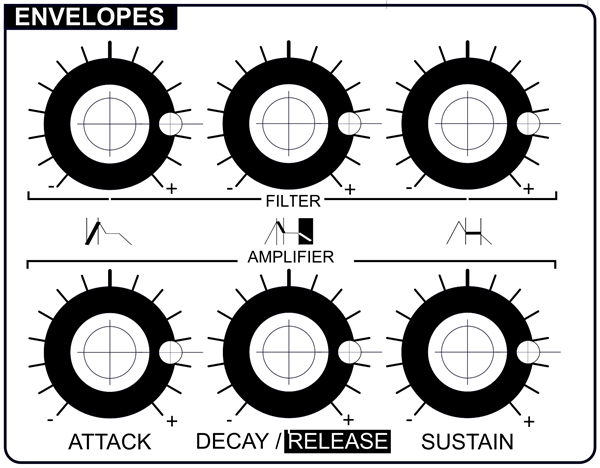

ENVELOPE GENERATORS (EGs) add motion to a sound after a note is played. The MiniZed Synth has two separate Envelope Generators that affect the brightness and loudness of
the MiniZed Synth's sound by modulating the Filter Cutoff and Volume.
The EGs are started by a Gate or MIDI Note message. Once started, their shape in time is set by the ATTACK, DECAY/RELEASE, and SUSTAIN controls, as well as the Release switch and length of the Note played.
Panel Controls for the Envelopes
FILTER ATTACK (CC# 23):
Sets the time it takes for the Attack portion of the Filter EG to rise from zero to maximum. The Attack time ranges from 1 msec to 30 seconds.
FILTER DECAY/RELEASE (CC# 24):
Sets the time for the Decay and Release portion of the Filter EG. When a note is held, and the Attack time end is reached, the Decay portion of the EG starts. During the Decay portion, the EG moves to the Sustain level. When a note is released, the EG moves back to zero at the rate set by this control. This time ranges from 1 msec to 30 seconds. The Release segment of the
The envelope is determined by the state of the RELEASE switch (ON/OFF).
FILTER SUSTAIN (CC# 25):
Sets the Filter EG level after the Decay and before the Release portion. A note must be held longer than both the Attack and Decay time to reach the Sustain level. The level is adjustable from 0 to 100%.
AMPLIFIER ATTACK (CC# 28):
Sets the time it takes for the Attack portion of the Amplifier EG to rise from zero to maximum. The Attack time ranges from 1 msec to 30 seconds.
AMPLIFIER DECAY/RELEASE (CC# 29):
Sets the time for the Decay and Release portion of the Amplifier EG.
When a note is held, and the Attack time end is reached, the Decay portion of the EG starts. During the decay portion, the EG moves to the Sustain level.
When a note is released, the EG moves back to zero at the rate set by this control. The time ranges from 1 msec to 30 seconds.
The Release segment of the Envelope is determined by the state of the RELEASE switch (ON/OFF).
AMPLIFIER SUSTAIN (CC# 30):
Sets the Amplifier EG level after the Decay and before the Release portion. A note must be held longer than both the Attack and Decay time to reach the Sustain level. The level is adjustable from 0 to 100%.
RELEASE
The RELEASE switch enables or disables the Release segment of both Envelope Generators.
When enabled, the Envelope Release time is the same as the Envelope Decay time, and the DECAY control adjusts the time for both segments.
When disabled, the Release segment does not occur and the Envelope stops abruptly in response to a “Note Off” message (or when the Gate goes to zero).
Modulation (MOD)
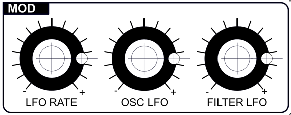
The MiniZed Synth's MODULATION section provides an LFO with adjustable RATE and AMOUNT controls for the oscillators and the Filter. The Low-Frequency Oscillator (LFO) is a signal used to move the pitch of Oscillators and the Filter Cutoff up and down automatically. An LFO can be used to simulate vibrato, create wobbling filter sweeps, or make interesting synthesizer sounds.
Panel Controls for the Modulation
LFO RATE (CC# 3):
Sets the frequency of LFO Modulation. The range is from 0.1Hz to 100Hz.
OSC LFO AMOUNT (CC# 13):
Sets the maximum amount the LFO moves the OSCILLATORS pitch up and down, up to +/- 1 octave. Modulation affects both Oscillators.
If using a MIDI controller, the Mod Wheel (CC# 1) is used to fade the LFO Pitch Modulation in and out.
FILTER LFO AMOUNT (CC# 12):
Sets the maximum amount the LFO moves the Filter Cutoff up and down, up to +/- 5 octaves. Amounts above 20KHz or below 20 Hz are clipped.
If using a MIDI controller, the Mod Wheel (CC# 1) is used to fade the LFO Filter Modulation in and out.
Amplifier Volume
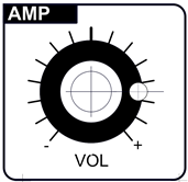
The MiniZed Synth features a monophonic Audio Output that is adjusted by the VOLUME control.
This is an external analog control to the MiniZed development board, intended to control an amplified output.
Panel Controls for the Amplifier Volume
VOLUME:
Adjusts the output of an amplified analog output.
Rotating the control fully clockwise produces the maximum output.
Rotating the control fully counterclockwise silences the MiniZed Synth.
4. High-Level Design

High-level MiniZed Synth Block Diagram. Heavy Blocks are custom blocks
The core of the synthesizer is the AVNET MiniZed development board. The kernel is divided into two main parts. A software program that runs on the Processing System (PS) part, based on the ARM 9 microcontroller, and a design built on top of the FPGA fabric.
The software program is in charge of configuring the oscillators, responding to user inputs from the front panel, and processing the MIDI orders, it interfaces between the MIDI controller devices and the synthesizer module created in the FPGA fabric as an accelerated hardware module.
To expand the user interface there are three new modules external to the MiniZed development board: an additional board with a 16:2 analog multiplexer that allows reading 16 analog potentiometers, a sound editing panel with 16 user-controlled analog potentiometers control, and an expansion board with 4 push buttons and 5 indicator LEDs.
Finally, there is another expansion board that allows the connection of standard MIDI controllers via a 5-pin DIN connector and another one with a Low Pass Filter plus amplifier to convert the Pulse Density Modulated (PDM ) signal generated by a 1-bit Delta Sigma Digital filter module into an analog signal. and amplify the signal sent to the speaker.
Communication with MIDI controllers can be done either through the DIN connector or a USB UART bridge taking advantage of the MiniZed's mini USB connector.
5. Hardware Accelerated Synth Module IP
The Synth Module IP is controlled from a bare metal application written in C that runs on Zynq's ARM 9 Microcontroller Processing System.
The system uses an AXI4 Lite Bus to communicate from the bare metal C app, without the support of a known operating system as FreeRTOS or Linux, to the Synth Module.
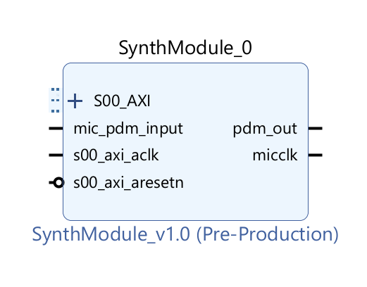
5.1. Custom Synth Module AXI4 Lite Peripheral IP
The Synth Module is packaged as a Vivado IP Block and is fully configured from the bare metal software application using AXI Lite 4 bus protocol.
It has one input for the 1-bit PDM built-in microphone and two outputs. One output with the 2.4 MHz generated microphone clock and the other is 1 bit PDM output sound signal.
If the reader is interested in the complete creation of an AXI4 Lite peripheral, I made a complete tutorial, see Arty S7 50 ArtyBot Custom AXI4 Lite IP Peripheral for Sensing Motor Rotational Speed
The Synth Module is coded in SystemVerilog:
`timescale 1ns / 1ps


module synth_module #(PHASE_ACC_WIDTH = 30)(
    input logic clk,
    input logic reset,
    // oscillator 1 configuration
    input logic [PHASE_ACC_WIDTH-1:0] osc1_fccw, // Pitch, oscillator 1 frequency carrier ctrl word
    input logic [PHASE_ACC_WIDTH-1:0] osc1_focw, // Detune, oscillator 1 frequency offset ctrl word
    input logic [PHASE_ACC_WIDTH-1:0] osc1_pho, // Phase shift, oscillator 1 phase offset ctrl word
    input logic [2:0] osc1_wt, // oscillator 1 wave type
    input logic [15:0] mix_lvl_osc1, // oscillator 1 volume level

    // oscillator 2 configuration
    input logic [PHASE_ACC_WIDTH-1:0] osc2_fccw, // Pitch, oscillator 1 frequency carrier ctrl word
    input logic [PHASE_ACC_WIDTH-1:0] osc2_focw, // Detune, oscillator 1 frequency offset ctrl word
    input logic [PHASE_ACC_WIDTH-1:0] osc2_pho, // Phase shift, oscillator 1 phase offset ctrl word
    input logic [2:0] osc2_wt, // oscillator 2 wave type
    input logic [15:0] mix_lvl_osc2, // oscillator 2 volume level

    // oscillator 3 / noise oscillator configuration
    input logic [PHASE_ACC_WIDTH-1:0] osc3_fccw, // Pitch, oscillator 1 frequency carrier ctrl word
    input logic [PHASE_ACC_WIDTH-1:0] osc3_focw, // Detune, oscillator 1 frequency offset ctrl word
    input logic [PHASE_ACC_WIDTH-1:0] osc3_pho, // Phase shift, oscillator 1 phase offset ctrl word
    input logic [2:0] osc3_wt, // oscillator 3 wave type
    input logic [15:0] mix_lvl_osc3, // oscillator 3 volume level

    // LFO oscillator configuration
    input logic [PHASE_ACC_WIDTH-1:0] lfoo_fccw, // LFO oscillator frequency carrier ctrl word
    input logic [PHASE_ACC_WIDTH-1:0] lfoo_focw, // LFO oscillator frequency offset ctrl word
    input logic [PHASE_ACC_WIDTH-1:0] lfoo_pho, // LFO oscillator phase offset ctrl word
    input logic [2:0] lfoo_wt, // LFO oscillator wave type
    input logic [15:0] lfoo_lvl, // Sets the maximum amount the LFO moves the VCOs pitch up and down, up to +/- 1 octave.

    // LFO filter configuration
    input logic [PHASE_ACC_WIDTH-1:0] lfof_fccw, // LFO filter frequency carrier ctrl word
    input logic [PHASE_ACC_WIDTH-1:0] lfof_focw, // LFO filter frequency offset ctrl word
    input logic [PHASE_ACC_WIDTH-1:0] lfof_pho, // LFO filter phase offset ctrl word
    input logic [2:0] lfof_wt, // LFO filter wave type
    input logic [15:0] lfof_lvl, // Sets the maximum amount the LFO moves the Filter Cutoff up and down, up to +/- 5 octaves.

    // Amplifier ADSR configuration
    input logic adsra_start, // generate a pulse to start the envelope generation
    input logic [31:0] adsra_a, // precalculated (Amax - 0)/(t_attack - t_sys) steps for the attack segment
    input logic [31:0] adsra_d,  // precalculated (A_max-A_sus) / (t_sustain / t_sys) steps for the decay segment
    input logic [31:0] adsra_sl, // amplitude for the sustain segment
    input logic [31:0] adsra_r,  // precalculated (A_sus - 0)/(t_release - t_sys) steps fot the release segment
    input logic [31:0] adsra_st, // tsustain / t_sys steps for the sustain

    // Filter ADSR configuration
    input logic adsrf_start, // generate a pulse to start the envelope generation
    input logic [31:0] adsrf_a, // precalculated (Amax - 0)/(t_attack - t_sys) steps for the attack segment
    input logic [31:0] adsrf_d,  // precalculated (A_max-A_sus) / (t_sustain / t_sys) steps for the decay segment
    input logic [31:0] adsrf_sl, // amplitude for the sustain segment
    input logic [31:0] adsrf_r,  // precalculated (A_sus - 0)/(t_release - t_sys) steps fot the release segment
    input logic [31:0] adsrf_st, // tsustain / t_sys steps for the sustain

    // Filter configuration
    input logic [31:0] fcut, // filter cutoff frequency
    input logic [31:0] fres, // filter resonance level
    input logic [31:0] feg, // filter envelope generator amount


    // PDM Microphone
    input logic mic_pdm_input, // Input external P1-bit DM MiniZed Signal AUDIO_DAT
    input logic [15:0] mix_lvl_mic, // oscillator 3 volume level

    output logic pdm_out, // 1-bit PDM sound output
    output logic mic_clk,  // generated microphone clock signal route to Minized external AUDIO_CLK

    output logic adsra_idle,
    output logic [15:0] adsra_amp


    );

    // signal declarations
    localparam BIAS = 2 ** (15); // {1'b1, (W-2){1'b0}};


    // constants for envelopes
    localparam MAX = 32'h8000_0000; // MAX volume
    localparam BYPASS = 32'hffff_ffff; // Bypass envelope
    localparam ZERO = 32'h0000_0000; // mute

    // constants for oscillators
    localparam SINE =     3'b000;
    localparam SQUARE =   3'b001;
    localparam SAW =      3'b010;
    localparam TRIANGLE = 3'b011;
    localparam NOISE =    3'b100;

    // lfo oscillator outputs
    logic [15:0] lfoo_output; // LFO oscillator output
    logic lfoo_pulse_out; //  LFO Oscillator pulse output

//    // lfo filter outputs
    logic [15:0] lfof_output; // lfo filter output
    logic lfof_pulse_out; //  Oscillator 1 pulse output


    // Oscillator 1 outputs
    logic [15:0] osc1_pcm_out; // Oscillator 1 PCM output
    logic osc1_pulse_out; //  Oscillator 1 pulse output

//    // Oscillator 2 outputs
    logic [15:0] osc2_pcm_out; // Oscillator 2 PCM output
    logic osc2_pulse_out; //  Oscillator 2 pulse output

//    // Noise / Oscillator 3 outputs
    logic [15:0] osc3_pcm_out; // Oscillator 3 PCM output
    logic osc3_pulse_out; //  Oscillator 3 pulse output

    // Microphone Outputs
    logic [15:0] mic_pcm_out; // Microphone PCM output
    logic mic_data_valid; //  Microphone PDM to PCM conversion data valid

    // Mixer outputs
    logic [15:0] mix_pcm_out; // Mixer PCM output

    // amplifier ADSR amplitude output
     logic [15:0] adsra_amp;
     logic [15:0] adsra_rt_amp;
     logic [15:0] adsra_selected;

     // filter ADSR amplitude output
     logic [15:0] adsrf_amp;
     logic [15:0] adsrf_rt_amp;
     logic [15:0] adsrf_selected;

    // Amplifier outputs
    logic [15:0] amp_pcm_out;

//    filter outputs
    logic [15:0] filter_pcm_out;


    logic [PHASE_ACC_WIDTH-1:0] lfoo_extended;
    logic [PHASE_ACC_WIDTH-1:0] lfof_extended;

    logic adsrf_idle;
    logic adsrf_rt_idle;
    logic adsrf_nrt_idle;

    logic adsra_rt_idle;
    logic adsra_nrt_idle;


//    // Keep The range is from 0.01Hz to 100Hz
//    // instantiate lfo oscillator
    ddfs #(.PHASE_ACC_WIDTH(PHASE_ACC_WIDTH)) lfoo(.clk(clk),
        .reset(reset),
        .freq_carrier_ctrl_word(lfoo_fccw),
        .freq_offset_ctrl_word(lfoo_focw),
        .phase_offset(lfoo_pho),
        .envelope(lfoo_lvl), // Amplitude modulation: envelope, digitized value of A(t) in Q2.14 format
        .pcm_out(lfoo_output),
        .pulse_out(lfoo_pulse_out),
        .wave_type( lfoo_wt)
        );

    // extend sign to 30 bits
    assign lfoo_extended = {{ 14{lfoo_output[15]}},lfoo_output};

    // extend sign to 30 bits
    assign lfof_extended = {{ 14{lfof_output[15]}},lfof_output};


//    // Keep The range is from up to +/- 5 octaves. Amounts above 20KHz or below 20 Hz are clipped
//    // instantiate lfo filter
    ddfs #(.PHASE_ACC_WIDTH(PHASE_ACC_WIDTH)) lfof(.clk(clk),
        .reset(reset),
        .freq_carrier_ctrl_word(lfof_fccw),
        .freq_offset_ctrl_word(lfof_focw),
        .phase_offset(lfof_pho),
        .envelope(lfof_lvl), // Amplitude modulation: envelope, digitized value of A(t) in Q2.14 format
        .pcm_out(lfof_output),
        .pulse_out(lfof_pulse_out),
        .wave_type( lfof_wt)
        );

    // instantiate oscillator 1 osc_1
    ddfs #(.PHASE_ACC_WIDTH(PHASE_ACC_WIDTH)) osc1(.clk(clk),
        .reset(reset),
        .freq_carrier_ctrl_word(osc1_fccw),// 4.724 .freq_carrier_ctrl_word(osc1_fccw),
        .freq_offset_ctrl_word(lfoo_extended),  // .freq_offset_ctrl_word(lfoo_output), // LFO moves the VCOs pitch up and down, up to +/- 1 octave
        .phase_offset(osc1_pho), // .phase_offset(osc1_pho),
        .envelope(16'h4000), // Amplitude modulation: envelope, digitized value of A(t) in Q2.14 format
        .pcm_out(osc1_pcm_out),
        .pulse_out(osc1_pulse_out),
        .wave_type(osc1_wt)//.wave_type( 3'b001)
        );

//   // instantiate oscillator 2 osc_2
    ddfs #(.PHASE_ACC_WIDTH(PHASE_ACC_WIDTH)) osc2(.clk(clk),
        .reset(reset),
        .freq_carrier_ctrl_word(osc2_fccw),
        .freq_offset_ctrl_word(lfoo_extended), // LFO moves the VCOs pitch up and down, up to +/- 1 octave
        .phase_offset(osc2_pho),
        .envelope(16'h4000), // Amplitude modulation: envelope, digitized value of A(t) in Q2.14 format
        .pcm_out(osc2_pcm_out),
        .pulse_out(osc2_pulse_out),
        .wave_type( osc2_wt)
        );

    // instantiate oscillator 3 osc_3 usually noise
    ddfs #(.PHASE_ACC_WIDTH(PHASE_ACC_WIDTH)) osc3(.clk(clk),
        .reset(reset),
        .freq_carrier_ctrl_word(osc3_fccw),
        .freq_offset_ctrl_word(lfoo_extended),
        .phase_offset(osc3_pho),
        .envelope(16'h4000), // Amplitude modulation: envelope, digitized value of A(t) in Q2.14 format
        .pcm_out(osc3_pcm_out),
        .pulse_out(osc3_pulse_out),
        .wave_type( osc3_wt)
        );

    // instantiate PDM to PCM converter for the microphone input
    pdm_microphone microphone(
        .clk(clk),
        .reset(reset),
        .mic_pdm_data(mic_pdm_input),
        .mic_pcm_data(mic_pcm_out),
        .mic_data_valid(mic_data_valid),
        .mic_clk(mic_clk)
    );

    // instantiate mixer
    mixer mix(.clk(clk),
        .reset(reset),
        .input_1(osc1_pcm_out),
        .lvl_1(mix_lvl_osc1),
        .input_2(osc2_pcm_out),
        .lvl_2(mix_lvl_osc2),
        .input_3(osc3_pcm_out),// .input_3(osc3_pcm_out),
        .lvl_3(mix_lvl_osc3),
        .input_4(mic_pcm_out),
        .lvl_4(mix_lvl_mic),
        .pcm_out(mix_pcm_out)
        );

     // if sustain time is  32'hffff_fff select real time mode ADSR
     always_comb begin
       if (adsra_st == 32'hffff_ffff) begin
            adsra_selected = adsra_rt_amp;
            adsrf_selected = adsrf_rt_amp;
       end else begin
            adsra_selected = adsra_amp;
            adsrf_selected = adsrf_amp;
       end
     end

     assign adsra_idle = adsra_nrt_idle & adsra_rt_idle & adsrf_nrt_idle & adsrf_rt_idle;


     // instantiate amplifier ADSR amplitude generator
      adsr adsra(
          .clk(clk),
          .reset(reset),
          .start(adsra_start), // generate a pulse to start the envelope generation
          .attack_step_value(adsra_a), // precalculated (Amax - 0)/(t_attack - t_sys) steps for the attack segment
          .decay_step_value(adsra_d),  // precalculated (A_max-A_sus) / (t_sustain / t_sys) steps for the decay segment
          .sustain_level(adsra_sl), // amplitude for the sustain segment
          .release_step_value(adsra_r),  // precalculated (A_sus - 0)/(t_release - t_sys) steps fot the release segment
          .sustain_time(adsra_st), // tsustain / t_sys steps for the sustain
          .envelope(adsra_amp),
          .adsr_idle(adsra_nrt_idle)
          );

      // instantiate amplifier ADSR real time mode amplitude generator
      adsr_rt adsra_rt(
          .clk(clk),
          .reset(reset),
          .start(adsra_start), // g adsr sustain active when start asserted
          .attack_step_value(adsra_a), // precalculated (Amax - 0)/(t_attack - t_sys) steps for the attack segment
          .decay_step_value(adsra_d),  // precalculated (A_max-A_sus) / (t_sustain / t_sys) steps for the decay segment
          .sustain_level(adsra_sl), // amplitude for the sustain segment
          .release_step_value(adsra_r),  // precalculated (A_sus - 0)/(t_release - t_sys) steps fot the release segment
          .envelope(adsra_rt_amp),
          .adsr_idle(adsra_rt_idle)
          );

//      // instantiate filter ADSR amplitude generator
      adsr adsrf(
          .clk(clk),
          .reset(reset),
          .start(adsrf_start), // generate a pulse to start the envelope generation
          .attack_step_value(adsrf_a), // precalculated (Amax - 0)/(t_attack - t_sys) steps for the attack segment
          .decay_step_value(adsrf_d),  // precalculated (A_max-A_sus) / (t_sustain / t_sys) steps for the decay segment
          .sustain_level(adsrf_sl), // amplitude for the sustain segment
          .release_step_value(adsrf_r),  // precalculated (A_sus - 0)/(t_release - t_sys) steps fot the release segment
          .sustain_time(adsrf_st), // tsustain / t_sys steps for the sustain
          .envelope(adsrf_amp),
          .adsr_idle(adsrf_nrt_idle)
          );

     adsr_rt adsrf_rt(
          .clk(clk),
          .reset(reset),
          .start(adsrf_start), // adsr sustain active when start asserted
          .attack_step_value(adsrf_a), // precalculated (Amax - 0)/(t_attack - t_sys) steps for the attack segment
          .decay_step_value(adsrf_d),  // precalculated (A_max-A_sus) / (t_sustain / t_sys) steps for the decay segment
          .sustain_level(adsrf_sl), // amplitude for the sustain segment
          .release_step_value(adsrf_r),  // precalculated (A_sus - 0)/(t_release - t_sys) steps fot the release segment
          .envelope(adsrf_rt_amp),
          .adsr_idle(adsrf_rt_idle)
          );

      // instantiate Amplifier
      amplifier amp(
          .clk(clk),
          .reset(reset),
          .pcm_input(mix_pcm_out),
          .envelope(adsra_selected),
          .pcm_out(amp_pcm_out));

//      // instantiate filter
      filter filter_unit(
          .clk(clk),
          .reset(reset),
          .fccw(osc1_fccw),
          .pcm_in(amp_pcm_out),
          .cutoff_freq(fcut),
          .resonance_lvl(fres),
          .eg_amount(feg), //EG AMOUNT Determines how much the Filter Envelope Generator (EG) adds to or subtracts from the Filter Cutoff control setting.
          .envelope(adsrf_rt_amp),
          .modulation(lfof_output),
          .pcm_out(filter_pcm_out)
      );

      // instantiate 1 bit delta sigma DAC
      ds_1bit_dac dac(
        .clk(clk),
        .reset(reset),
        .pcm_in(filter_pcm_out),
        .pdm_out(pdm_out)
        );


endmodule
SynthModuleAxi
`timescale 1 ns / 1 ps
module SynthModule_v1_0_S00_AXI #
(
// Users to add parameters here
// User parameters ends
// Do not modify the parameters beyond this line
// Width of S_AXI data bus
parameter integer C_S_AXI_DATA_WIDTH = 32,
// Width of S_AXI address bus
parameter integer C_S_AXI_ADDR_WIDTH = 8
)
(
// Input external P1-bit DM MiniZed Signal AUDIO_DAT
input wire mic_pdm_input,
// 1-bit PDM sound output
output wire pdm_out, // 1-bit PDM sound output
// generated microphone clock signal route to Minized external AUDIO_CLK
output wire micclk,
output wire [31:0] osc1Freq,
// User ports ends
// Do not modify the ports beyond this line
// Global Clock Signal
input wire S_AXI_ACLK,
// Global Reset Signal. This Signal is Active LOW
input wire S_AXI_ARESETN,
// Write address (issued by master, acceped by Slave)
input wire [C_S_AXI_ADDR_WIDTH-1 : 0] S_AXI_AWADDR,
// Write channel Protection type. This signal indicates the
// privilege and security level of the transaction, and whether
// the transaction is a data access or an instruction access.
input wire [2 : 0] S_AXI_AWPROT,
// Write address valid. This signal indicates that the master signaling
// valid write address and control information.
input wire S_AXI_AWVALID,
// Write address ready. This signal indicates that the slave is ready
// to accept an address and associated control signals.
output wire S_AXI_AWREADY,
// Write data (issued by master, acceped by Slave)
input wire [C_S_AXI_DATA_WIDTH-1 : 0] S_AXI_WDATA,
// Write strobes. This signal indicates which byte lanes hold
// valid data. There is one write strobe bit for each eight
// bits of the write data bus.
input wire [(C_S_AXI_DATA_WIDTH/8)-1 : 0] S_AXI_WSTRB,
// Write valid. This signal indicates that valid write
// data and strobes are available.
input wire S_AXI_WVALID,
// Write ready. This signal indicates that the slave
// can accept the write data.
output wire S_AXI_WREADY,
// Write response. This signal indicates the status
// of the write transaction.
output wire [1 : 0] S_AXI_BRESP,
// Write response valid. This signal indicates that the channel
// is signaling a valid write response.
output wire S_AXI_BVALID,
// Response ready. This signal indicates that the master
// can accept a write response.
input wire S_AXI_BREADY,
// Read address (issued by master, acceped by Slave)
input wire [C_S_AXI_ADDR_WIDTH-1 : 0] S_AXI_ARADDR,
// Protection type. This signal indicates the privilege
// and security level of the transaction, and whether the
// transaction is a data access or an instruction access.
input wire [2 : 0] S_AXI_ARPROT,
// Read address valid. This signal indicates that the channel
// is signaling valid read address and control information.
input wire S_AXI_ARVALID,
// Read address ready. This signal indicates that the slave is
// ready to accept an address and associated control signals.
output wire S_AXI_ARREADY,
// Read data (issued by slave)
output wire [C_S_AXI_DATA_WIDTH-1 : 0] S_AXI_RDATA,
// Read response. This signal indicates the status of the
// read transfer.
output wire [1 : 0] S_AXI_RRESP,
// Read valid. This signal indicates that the channel is
// signaling the required read data.
output wire S_AXI_RVALID,
// Read ready. This signal indicates that the master can
// accept the read data and response information.
input wire S_AXI_RREADY
);
// AXI4LITE signals
reg [C_S_AXI_ADDR_WIDTH-1 : 0] axi_awaddr;
reg axi_awready;
reg axi_wready;
reg [1 : 0] axi_bresp;
reg axi_bvalid;
reg [C_S_AXI_ADDR_WIDTH-1 : 0] axi_araddr;
reg axi_arready;
reg [C_S_AXI_DATA_WIDTH-1 : 0] axi_rdata;
reg [1 : 0] axi_rresp;
reg axi_rvalid;
// Example-specific design signals
// local parameter for addressing 32 bit / 64 bit C_S_AXI_DATA_WIDTH
// ADDR_LSB is used for addressing 32/64 bit registers/memories
// ADDR_LSB = 2 for 32 bits (n downto 2)
// ADDR_LSB = 3 for 64 bits (n downto 3)
localparam integer ADDR_LSB = (C_S_AXI_DATA_WIDTH/32) + 1;
localparam integer OPT_MEM_ADDR_BITS = 5;
//----------------------------------------------
//-- Signals for user logic register space example
//------------------------------------------------
//-- Number of Slave Registers 34
reg [C_S_AXI_DATA_WIDTH-1:0] slv_reg0;
reg [C_S_AXI_DATA_WIDTH-1:0] slv_reg1;
reg [C_S_AXI_DATA_WIDTH-1:0] slv_reg2;
reg [C_S_AXI_DATA_WIDTH-1:0] slv_reg3;
reg [C_S_AXI_DATA_WIDTH-1:0] slv_reg4;
reg [C_S_AXI_DATA_WIDTH-1:0] slv_reg5;
reg [C_S_AXI_DATA_WIDTH-1:0] slv_reg6;
reg [C_S_AXI_DATA_WIDTH-1:0] slv_reg7;
reg [C_S_AXI_DATA_WIDTH-1:0] slv_reg8;
reg [C_S_AXI_DATA_WIDTH-1:0] slv_reg9;
reg [C_S_AXI_DATA_WIDTH-1:0] slv_reg10;
reg [C_S_AXI_DATA_WIDTH-1:0] slv_reg11;
reg [C_S_AXI_DATA_WIDTH-1:0] slv_reg12;
reg [C_S_AXI_DATA_WIDTH-1:0] slv_reg13;
reg [C_S_AXI_DATA_WIDTH-1:0] slv_reg14;
reg [C_S_AXI_DATA_WIDTH-1:0] slv_reg15;
reg [C_S_AXI_DATA_WIDTH-1:0] slv_reg16;
reg [C_S_AXI_DATA_WIDTH-1:0] slv_reg17;
reg [C_S_AXI_DATA_WIDTH-1:0] slv_reg18;
reg [C_S_AXI_DATA_WIDTH-1:0] slv_reg19;
reg [C_S_AXI_DATA_WIDTH-1:0] slv_reg20;
reg [C_S_AXI_DATA_WIDTH-1:0] slv_reg21;
reg [C_S_AXI_DATA_WIDTH-1:0] slv_reg22;
reg [C_S_AXI_DATA_WIDTH-1:0] slv_reg23;
reg [C_S_AXI_DATA_WIDTH-1:0] slv_reg24;
reg [C_S_AXI_DATA_WIDTH-1:0] slv_reg25;
reg [C_S_AXI_DATA_WIDTH-1:0] slv_reg26;
reg [C_S_AXI_DATA_WIDTH-1:0] slv_reg27;
reg [C_S_AXI_DATA_WIDTH-1:0] slv_reg28;
reg [C_S_AXI_DATA_WIDTH-1:0] slv_reg29;
reg [C_S_AXI_DATA_WIDTH-1:0] slv_reg30;
reg [C_S_AXI_DATA_WIDTH-1:0] slv_reg31;
reg [C_S_AXI_DATA_WIDTH-1:0] slv_reg32;
wire [C_S_AXI_DATA_WIDTH-1:0] slv_reg33;
wire slv_reg_rden;
wire slv_reg_wren;
reg [C_S_AXI_DATA_WIDTH-1:0] reg_data_out;
integer byte_index;
reg aw_en;
// I/O Connections assignments
assign S_AXI_AWREADY = axi_awready;
assign S_AXI_WREADY = axi_wready;
assign S_AXI_BRESP = axi_bresp;
assign S_AXI_BVALID = axi_bvalid;
assign S_AXI_ARREADY = axi_arready;
assign S_AXI_RDATA = axi_rdata;
assign S_AXI_RRESP = axi_rresp;
assign S_AXI_RVALID = axi_rvalid;
// Implement axi_awready generation
// axi_awready is asserted for one S_AXI_ACLK clock cycle when both
// S_AXI_AWVALID and S_AXI_WVALID are asserted. axi_awready is
// de-asserted when reset is low.
always @( posedge S_AXI_ACLK )
begin
if ( S_AXI_ARESETN == 1'b0 )
begin
axi_awready <= 1'b0;
aw_en <= 1'b1;
end
else
begin
if (~axi_awready && S_AXI_AWVALID && S_AXI_WVALID && aw_en)
begin
// slave is ready to accept write address when
// there is a valid write address and write data
// on the write address and data bus. This design
// expects no outstanding transactions.
axi_awready <= 1'b1;
aw_en <= 1'b0;
end
else if (S_AXI_BREADY && axi_bvalid)
begin
aw_en <= 1'b1;
axi_awready <= 1'b0;
end
else
begin
axi_awready <= 1'b0;
end
end
end
// Implement axi_awaddr latching
// This process is used to latch the address when both
// S_AXI_AWVALID and S_AXI_WVALID are valid.
always @( posedge S_AXI_ACLK )
begin
if ( S_AXI_ARESETN == 1'b0 )
begin
axi_awaddr <= 0;
end
else
begin
if (~axi_awready && S_AXI_AWVALID && S_AXI_WVALID && aw_en)
begin
// Write Address latching
axi_awaddr <= S_AXI_AWADDR;
end
end
end
// Implement axi_wready generation
// axi_wready is asserted for one S_AXI_ACLK clock cycle when both
// S_AXI_AWVALID and S_AXI_WVALID are asserted. axi_wready is
// de-asserted when reset is low.
always @( posedge S_AXI_ACLK )
begin
if ( S_AXI_ARESETN == 1'b0 )
begin
axi_wready <= 1'b0;
end
else
begin
if (~axi_wready && S_AXI_WVALID && S_AXI_AWVALID && aw_en )
begin
// slave is ready to accept write data when
// there is a valid write address and write data
// on the write address and data bus. This design
// expects no outstanding transactions.
axi_wready <= 1'b1;
end
else
begin
axi_wready <= 1'b0;
end
end
end
// Implement memory mapped register select and write logic generation
// The write data is accepted and written to memory mapped registers when
// axi_awready, S_AXI_WVALID, axi_wready and S_AXI_WVALID are asserted. Write strobes are used to
// select byte enables of slave registers while writing.
// These registers are cleared when reset (active low) is applied.
// Slave register write enable is asserted when valid address and data are available
// and the slave is ready to accept the write address and write data.
assign slv_reg_wren = axi_wready && S_AXI_WVALID && axi_awready && S_AXI_AWVALID;
always @( posedge S_AXI_ACLK )
begin
if ( S_AXI_ARESETN == 1'b0 )
begin
slv_reg0 <= 0;
slv_reg1 <= 0;
slv_reg2 <= 0;
slv_reg3 <= 0;
slv_reg4 <= 0;
slv_reg5 <= 0;
slv_reg6 <= 0;
slv_reg7 <= 0;
slv_reg8 <= 0;
slv_reg9 <= 0;
slv_reg10 <= 0;
slv_reg11 <= 0;
slv_reg12 <= 0;
slv_reg13 <= 0;
slv_reg14 <= 0;
slv_reg15 <= 0;
slv_reg16 <= 0;
slv_reg17 <= 0;
slv_reg18 <= 0;
slv_reg19 <= 0;
slv_reg20 <= 0;
slv_reg21 <= 0;
slv_reg22 <= 0;
slv_reg23 <= 0;
slv_reg24 <= 0;
slv_reg25 <= 0;
slv_reg26 <= 0;
slv_reg27 <= 0;
slv_reg28 <= 0;
slv_reg29 <= 0;
slv_reg30 <= 0;
slv_reg31 <= 0;
slv_reg32 <= 0;
// slv_reg33 <= 0; // assigned in user logic
end
else begin
if (slv_reg_wren)
begin
case ( axi_awaddr[ADDR_LSB+OPT_MEM_ADDR_BITS:ADDR_LSB] )
6'h00:
for ( byte_index = 0; byte_index <= (C_S_AXI_DATA_WIDTH/8)-1; byte_index = byte_index+1 )
if ( S_AXI_WSTRB[byte_index] == 1 ) begin
// Respective byte enables are asserted as per write strobes
// Slave register 0
slv_reg0[(byte_index*8) +: 8] <= S_AXI_WDATA[(byte_index*8) +: 8];
end
6'h01:
for ( byte_index = 0; byte_index <= (C_S_AXI_DATA_WIDTH/8)-1; byte_index = byte_index+1 )
if ( S_AXI_WSTRB[byte_index] == 1 ) begin
// Respective byte enables are asserted as per write strobes
// Slave register 1
slv_reg1[(byte_index*8) +: 8] <= S_AXI_WDATA[(byte_index*8) +: 8];
end
6'h02:
for ( byte_index = 0; byte_index <= (C_S_AXI_DATA_WIDTH/8)-1; byte_index = byte_index+1 )
if ( S_AXI_WSTRB[byte_index] == 1 ) begin
// Respective byte enables are asserted as per write strobes
// Slave register 2
slv_reg2[(byte_index*8) +: 8] <= S_AXI_WDATA[(byte_index*8) +: 8];
end
6'h03:
for ( byte_index = 0; byte_index <= (C_S_AXI_DATA_WIDTH/8)-1; byte_index = byte_index+1 )
if ( S_AXI_WSTRB[byte_index] == 1 ) begin
// Respective byte enables are asserted as per write strobes
// Slave register 3
slv_reg3[(byte_index*8) +: 8] <= S_AXI_WDATA[(byte_index*8) +: 8];
end
6'h04:
for ( byte_index = 0; byte_index <= (C_S_AXI_DATA_WIDTH/8)-1; byte_index = byte_index+1 )
if ( S_AXI_WSTRB[byte_index] == 1 ) begin
// Respective byte enables are asserted as per write strobes
// Slave register 4
slv_reg4[(byte_index*8) +: 8] <= S_AXI_WDATA[(byte_index*8) +: 8];
end
6'h05:
for ( byte_index = 0; byte_index <= (C_S_AXI_DATA_WIDTH/8)-1; byte_index = byte_index+1 )
if ( S_AXI_WSTRB[byte_index] == 1 ) begin
// Respective byte enables are asserted as per write strobes
// Slave register 5
slv_reg5[(byte_index*8) +: 8] <= S_AXI_WDATA[(byte_index*8) +: 8];
end
6'h06:
for ( byte_index = 0; byte_index <= (C_S_AXI_DATA_WIDTH/8)-1; byte_index = byte_index+1 )
if ( S_AXI_WSTRB[byte_index] == 1 ) begin
// Respective byte enables are asserted as per write strobes
// Slave register 6
slv_reg6[(byte_index*8) +: 8] <= S_AXI_WDATA[(byte_index*8) +: 8];
end
6'h07:
for ( byte_index = 0; byte_index <= (C_S_AXI_DATA_WIDTH/8)-1; byte_index = byte_index+1 )
if ( S_AXI_WSTRB[byte_index] == 1 ) begin
// Respective byte enables are asserted as per write strobes
// Slave register 7
slv_reg7[(byte_index*8) +: 8] <= S_AXI_WDATA[(byte_index*8) +: 8];
end
6'h08:
for ( byte_index = 0; byte_index <= (C_S_AXI_DATA_WIDTH/8)-1; byte_index = byte_index+1 )
if ( S_AXI_WSTRB[byte_index] == 1 ) begin
// Respective byte enables are asserted as per write strobes
// Slave register 8
slv_reg8[(byte_index*8) +: 8] <= S_AXI_WDATA[(byte_index*8) +: 8];
end
6'h09:
for ( byte_index = 0; byte_index <= (C_S_AXI_DATA_WIDTH/8)-1; byte_index = byte_index+1 )
if ( S_AXI_WSTRB[byte_index] == 1 ) begin
// Respective byte enables are asserted as per write strobes
// Slave register 9
slv_reg9[(byte_index*8) +: 8] <= S_AXI_WDATA[(byte_index*8) +: 8];
end
6'h0A:
for ( byte_index = 0; byte_index <= (C_S_AXI_DATA_WIDTH/8)-1; byte_index = byte_index+1 )
if ( S_AXI_WSTRB[byte_index] == 1 ) begin
// Respective byte enables are asserted as per write strobes
// Slave register 10
slv_reg10[(byte_index*8) +: 8] <= S_AXI_WDATA[(byte_index*8) +: 8];
end
6'h0B:
for ( byte_index = 0; byte_index <= (C_S_AXI_DATA_WIDTH/8)-1; byte_index = byte_index+1 )
if ( S_AXI_WSTRB[byte_index] == 1 ) begin
// Respective byte enables are asserted as per write strobes
// Slave register 11
slv_reg11[(byte_index*8) +: 8] <= S_AXI_WDATA[(byte_index*8) +: 8];
end
6'h0C:
for ( byte_index = 0; byte_index <= (C_S_AXI_DATA_WIDTH/8)-1; byte_index = byte_index+1 )
if ( S_AXI_WSTRB[byte_index] == 1 ) begin
// Respective byte enables are asserted as per write strobes
// Slave register 12
slv_reg12[(byte_index*8) +: 8] <= S_AXI_WDATA[(byte_index*8) +: 8];
end
6'h0D:
for ( byte_index = 0; byte_index <= (C_S_AXI_DATA_WIDTH/8)-1; byte_index = byte_index+1 )
if ( S_AXI_WSTRB[byte_index] == 1 ) begin
// Respective byte enables are asserted as per write strobes
// Slave register 13
slv_reg13[(byte_index*8) +: 8] <= S_AXI_WDATA[(byte_index*8) +: 8];
end
6'h0E:
for ( byte_index = 0; byte_index <= (C_S_AXI_DATA_WIDTH/8)-1; byte_index = byte_index+1 )
if ( S_AXI_WSTRB[byte_index] == 1 ) begin
// Respective byte enables are asserted as per write strobes
// Slave register 14
slv_reg14[(byte_index*8) +: 8] <= S_AXI_WDATA[(byte_index*8) +: 8];
end
6'h0F:
for ( byte_index = 0; byte_index <= (C_S_AXI_DATA_WIDTH/8)-1; byte_index = byte_index+1 )
if ( S_AXI_WSTRB[byte_index] == 1 ) begin
// Respective byte enables are asserted as per write strobes
// Slave register 15
slv_reg15[(byte_index*8) +: 8] <= S_AXI_WDATA[(byte_index*8) +: 8];
end
6'h10:
for ( byte_index = 0; byte_index <= (C_S_AXI_DATA_WIDTH/8)-1; byte_index = byte_index+1 )
if ( S_AXI_WSTRB[byte_index] == 1 ) begin
// Respective byte enables are asserted as per write strobes
// Slave register 16
slv_reg16[(byte_index*8) +: 8] <= S_AXI_WDATA[(byte_index*8) +: 8];
end
6'h11:
for ( byte_index = 0; byte_index <= (C_S_AXI_DATA_WIDTH/8)-1; byte_index = byte_index+1 )
if ( S_AXI_WSTRB[byte_index] == 1 ) begin
// Respective byte enables are asserted as per write strobes
// Slave register 17
slv_reg17[(byte_index*8) +: 8] <= S_AXI_WDATA[(byte_index*8) +: 8];
end
6'h12:
for ( byte_index = 0; byte_index <= (C_S_AXI_DATA_WIDTH/8)-1; byte_index = byte_index+1 )
if ( S_AXI_WSTRB[byte_index] == 1 ) begin
// Respective byte enables are asserted as per write strobes
// Slave register 18
slv_reg18[(byte_index*8) +: 8] <= S_AXI_WDATA[(byte_index*8) +: 8];
end
6'h13:
for ( byte_index = 0; byte_index <= (C_S_AXI_DATA_WIDTH/8)-1; byte_index = byte_index+1 )
if ( S_AXI_WSTRB[byte_index] == 1 ) begin
// Respective byte enables are asserted as per write strobes
// Slave register 19
slv_reg19[(byte_index*8) +: 8] <= S_AXI_WDATA[(byte_index*8) +: 8];
end
6'h14:
for ( byte_index = 0; byte_index <= (C_S_AXI_DATA_WIDTH/8)-1; byte_index = byte_index+1 )
if ( S_AXI_WSTRB[byte_index] == 1 ) begin
// Respective byte enables are asserted as per write strobes
// Slave register 20
slv_reg20[(byte_index*8) +: 8] <= S_AXI_WDATA[(byte_index*8) +: 8];
end
6'h15:
for ( byte_index = 0; byte_index <= (C_S_AXI_DATA_WIDTH/8)-1; byte_index = byte_index+1 )
if ( S_AXI_WSTRB[byte_index] == 1 ) begin
// Respective byte enables are asserted as per write strobes
// Slave register 21
slv_reg21[(byte_index*8) +: 8] <= S_AXI_WDATA[(byte_index*8) +: 8];
end
6'h16:
for ( byte_index = 0; byte_index <= (C_S_AXI_DATA_WIDTH/8)-1; byte_index = byte_index+1 )
if ( S_AXI_WSTRB[byte_index] == 1 ) begin
// Respective byte enables are asserted as per write strobes
// Slave register 22
slv_reg22[(byte_index*8) +: 8] <= S_AXI_WDATA[(byte_index*8) +: 8];
end
6'h17:
for ( byte_index = 0; byte_index <= (C_S_AXI_DATA_WIDTH/8)-1; byte_index = byte_index+1 )
if ( S_AXI_WSTRB[byte_index] == 1 ) begin
// Respective byte enables are asserted as per write strobes
// Slave register 23
slv_reg23[(byte_index*8) +: 8] <= S_AXI_WDATA[(byte_index*8) +: 8];
end
6'h18:
for ( byte_index = 0; byte_index <= (C_S_AXI_DATA_WIDTH/8)-1; byte_index = byte_index+1 )
if ( S_AXI_WSTRB[byte_index] == 1 ) begin
// Respective byte enables are asserted as per write strobes
// Slave register 24
slv_reg24[(byte_index*8) +: 8] <= S_AXI_WDATA[(byte_index*8) +: 8];
end
6'h19:
for ( byte_index = 0; byte_index <= (C_S_AXI_DATA_WIDTH/8)-1; byte_index = byte_index+1 )
if ( S_AXI_WSTRB[byte_index] == 1 ) begin
// Respective byte enables are asserted as per write strobes
// Slave register 25
slv_reg25[(byte_index*8) +: 8] <= S_AXI_WDATA[(byte_index*8) +: 8];
end
6'h1A:
for ( byte_index = 0; byte_index <= (C_S_AXI_DATA_WIDTH/8)-1; byte_index = byte_index+1 )
if ( S_AXI_WSTRB[byte_index] == 1 ) begin
// Respective byte enables are asserted as per write strobes
// Slave register 26
slv_reg26[(byte_index*8) +: 8] <= S_AXI_WDATA[(byte_index*8) +: 8];
end
6'h1B:
for ( byte_index = 0; byte_index <= (C_S_AXI_DATA_WIDTH/8)-1; byte_index = byte_index+1 )
if ( S_AXI_WSTRB[byte_index] == 1 ) begin
// Respective byte enables are asserted as per write strobes
// Slave register 27
slv_reg27[(byte_index*8) +: 8] <= S_AXI_WDATA[(byte_index*8) +: 8];
end
6'h1C:
for ( byte_index = 0; byte_index <= (C_S_AXI_DATA_WIDTH/8)-1; byte_index = byte_index+1 )
if ( S_AXI_WSTRB[byte_index] == 1 ) begin
// Respective byte enables are asserted as per write strobes
// Slave register 28
slv_reg28[(byte_index*8) +: 8] <= S_AXI_WDATA[(byte_index*8) +: 8];
end
6'h1D:
for ( byte_index = 0; byte_index <= (C_S_AXI_DATA_WIDTH/8)-1; byte_index = byte_index+1 )
if ( S_AXI_WSTRB[byte_index] == 1 ) begin
// Respective byte enables are asserted as per write strobes
// Slave register 29
slv_reg29[(byte_index*8) +: 8] <= S_AXI_WDATA[(byte_index*8) +: 8];
end
6'h1E:
for ( byte_index = 0; byte_index <= (C_S_AXI_DATA_WIDTH/8)-1; byte_index = byte_index+1 )
if ( S_AXI_WSTRB[byte_index] == 1 ) begin
// Respective byte enables are asserted as per write strobes
// Slave register 30
slv_reg30[(byte_index*8) +: 8] <= S_AXI_WDATA[(byte_index*8) +: 8];
end
6'h1F:
for ( byte_index = 0; byte_index <= (C_S_AXI_DATA_WIDTH/8)-1; byte_index = byte_index+1 )
if ( S_AXI_WSTRB[byte_index] == 1 ) begin
// Respective byte enables are asserted as per write strobes
// Slave register 31
slv_reg31[(byte_index*8) +: 8] <= S_AXI_WDATA[(byte_index*8) +: 8];
end
6'h20:
for ( byte_index = 0; byte_index <= (C_S_AXI_DATA_WIDTH/8)-1; byte_index = byte_index+1 )
if ( S_AXI_WSTRB[byte_index] == 1 ) begin
// Respective byte enables are asserted as per write strobes
// Slave register 32
slv_reg32[(byte_index*8) +: 8] <= S_AXI_WDATA[(byte_index*8) +: 8];
end
6'h21:
for ( byte_index = 0; byte_index <= (C_S_AXI_DATA_WIDTH/8)-1; byte_index = byte_index+1 )
if ( S_AXI_WSTRB[byte_index] == 1 ) begin
// Respective byte enables are asserted as per write strobes
// Slave register 33
// slv_reg33[(byte_index*8) +: 8] <= S_AXI_WDATA[(byte_index*8) +: 8]; // assigned in user logic
end
default : begin
slv_reg0 <= slv_reg0;
slv_reg1 <= slv_reg1;
slv_reg2 <= slv_reg2;
slv_reg3 <= slv_reg3;
slv_reg4 <= slv_reg4;
slv_reg5 <= slv_reg5;
slv_reg6 <= slv_reg6;
slv_reg7 <= slv_reg7;
slv_reg8 <= slv_reg8;
slv_reg9 <= slv_reg9;
slv_reg10 <= slv_reg10;
slv_reg11 <= slv_reg11;
slv_reg12 <= slv_reg12;
slv_reg13 <= slv_reg13;
slv_reg14 <= slv_reg14;
slv_reg15 <= slv_reg15;
slv_reg16 <= slv_reg16;
slv_reg17 <= slv_reg17;
slv_reg18 <= slv_reg18;
slv_reg19 <= slv_reg19;
slv_reg20 <= slv_reg20;
slv_reg21 <= slv_reg21;
slv_reg22 <= slv_reg22;
slv_reg23 <= slv_reg23;
slv_reg24 <= slv_reg24;
slv_reg25 <= slv_reg25;
slv_reg26 <= slv_reg26;
slv_reg27 <= slv_reg27;
slv_reg28 <= slv_reg28;
slv_reg29 <= slv_reg29;
slv_reg30 <= slv_reg30;
slv_reg31 <= slv_reg31;
slv_reg32 <= slv_reg32;
// slv_reg33 <= slv_reg33; // assigned in user logic
end
endcase
end
end
end
// Implement write response logic generation
// The write response and response valid signals are asserted by the slave
// when axi_wready, S_AXI_WVALID, axi_wready and S_AXI_WVALID are asserted.
// This marks the acceptance of address and indicates the status of
// write transaction.
always @( posedge S_AXI_ACLK )
begin
if ( S_AXI_ARESETN == 1'b0 )
begin
axi_bvalid <= 0;
axi_bresp <= 2'b0;
end
else
begin
if (axi_awready && S_AXI_AWVALID && ~axi_bvalid && axi_wready && S_AXI_WVALID)
begin
// indicates a valid write response is available
axi_bvalid <= 1'b1;
axi_bresp <= 2'b0; // 'OKAY' response
end // work error responses in future
else
begin
if (S_AXI_BREADY && axi_bvalid)
//check if bready is asserted while bvalid is high)
//(there is a possibility that bready is always asserted high)
begin
axi_bvalid <= 1'b0;
end
end
end
end
// Implement axi_arready generation
// axi_arready is asserted for one S_AXI_ACLK clock cycle when
// S_AXI_ARVALID is asserted. axi_awready is
// de-asserted when reset (active low) is asserted.
// The read address is also latched when S_AXI_ARVALID is
// asserted. axi_araddr is reset to zero on reset assertion.
always @( posedge S_AXI_ACLK )
begin
if ( S_AXI_ARESETN == 1'b0 )
begin
axi_arready <= 1'b0;
axi_araddr <= 32'b0;
end
else
begin
if (~axi_arready && S_AXI_ARVALID)
begin
// indicates that the slave has acceped the valid read address
axi_arready <= 1'b1;
// Read address latching
axi_araddr <= S_AXI_ARADDR;
end
else
begin
axi_arready <= 1'b0;
end
end
end
// Implement axi_arvalid generation
// axi_rvalid is asserted for one S_AXI_ACLK clock cycle when both
// S_AXI_ARVALID and axi_arready are asserted. The slave registers
// data are available on the axi_rdata bus at this instance. The
// assertion of axi_rvalid marks the validity of read data on the
// bus and axi_rresp indicates the status of read transaction.axi_rvalid
// is deasserted on reset (active low). axi_rresp and axi_rdata are
// cleared to zero on reset (active low).
always @( posedge S_AXI_ACLK )
begin
if ( S_AXI_ARESETN == 1'b0 )
begin
axi_rvalid <= 0;
axi_rresp <= 0;
end
else
begin
if (axi_arready && S_AXI_ARVALID && ~axi_rvalid)
begin
// Valid read data is available at the read data bus
axi_rvalid <= 1'b1;
axi_rresp <= 2'b0; // 'OKAY' response
end
else if (axi_rvalid && S_AXI_RREADY)
begin
// Read data is accepted by the master
axi_rvalid <= 1'b0;
end
end
end
// Implement memory mapped register select and read logic generation
// Slave register read enable is asserted when valid address is available
// and the slave is ready to accept the read address.
assign slv_reg_rden = axi_arready & S_AXI_ARVALID & ~axi_rvalid;
always @(*)
begin
// Address decoding for reading registers
case ( axi_araddr[ADDR_LSB+OPT_MEM_ADDR_BITS:ADDR_LSB] )
6'h00 : reg_data_out <= slv_reg0;
6'h01 : reg_data_out <= slv_reg1;
6'h02 : reg_data_out <= slv_reg2;
6'h03 : reg_data_out <= slv_reg3;
6'h04 : reg_data_out <= slv_reg4;
6'h05 : reg_data_out <= slv_reg5;
6'h06 : reg_data_out <= slv_reg6;
6'h07 : reg_data_out <= slv_reg7;
6'h08 : reg_data_out <= slv_reg8;
6'h09 : reg_data_out <= slv_reg9;
6'h0A : reg_data_out <= slv_reg10;
6'h0B : reg_data_out <= slv_reg11;
6'h0C : reg_data_out <= slv_reg12;
6'h0D : reg_data_out <= slv_reg13;
6'h0E : reg_data_out <= slv_reg14;
6'h0F : reg_data_out <= slv_reg15;
6'h10 : reg_data_out <= slv_reg16;
6'h11 : reg_data_out <= slv_reg17;
6'h12 : reg_data_out <= slv_reg18;
6'h13 : reg_data_out <= slv_reg19;
6'h14 : reg_data_out <= slv_reg20;
6'h15 : reg_data_out <= slv_reg21;
6'h16 : reg_data_out <= slv_reg22;
6'h17 : reg_data_out <= slv_reg23;
6'h18 : reg_data_out <= slv_reg24;
6'h19 : reg_data_out <= slv_reg25;
6'h1A : reg_data_out <= slv_reg26;
6'h1B : reg_data_out <= slv_reg27;
6'h1C : reg_data_out <= slv_reg28;
6'h1D : reg_data_out <= slv_reg29;
6'h1E : reg_data_out <= slv_reg30;
6'h1F : reg_data_out <= slv_reg31;
6'h20 : reg_data_out <= slv_reg32;
6'h21 : reg_data_out <= slv_reg33;
default : reg_data_out <= 0;
endcase
end
// Output register or memory read data
always @( posedge S_AXI_ACLK )
begin
if ( S_AXI_ARESETN == 1'b0 )
begin
axi_rdata <= 0;
end
else
begin
// When there is a valid read address (S_AXI_ARVALID) with
// acceptance of read address by the slave (axi_arready),
// output the read dada
if (slv_reg_rden)
begin
axi_rdata <= reg_data_out; // register read data
end
end
end
// Add user logic here
//Register 0: Gates Register {30'b0, adsrf_start,adsra_start}
//bit 0: adsra_start, generate a pulse to start the oscillator envelope generation
wire adsra_start;
assign adsra_start = slv_reg0[0];
//bit 1: adsrf_start, generate a pulse to start the filter envelope generation
wire adsrf_start;
assign adsrf_start = slv_reg0[1];
//Register 1 :osc1_fccw
//bits 29 to 0: osc1_fccw 30-bits Pitch, oscillator 1 frequency carrier ctrl word
wire [29:0] osc1_fccw;
assign osc1_fccw = slv_reg1[29:0];
//Register 2 :osc1_focw
//bits 29 to 0: osc1_focw 30-bits Detune, oscillator 1 frequency offset ctrl word
wire [29:0] osc1_focw;
assign osc1_focw = slv_reg2[29:0];
//Register 3: osc1_pho:
//bits 29 to 0: osc1_pho, Phase shift, oscillator 1 phase offset ctrl word
wire [29:0] osc1_pho;
assign osc1_pho = slv_reg3[29:0];
//Register 4 :osc2_fccw:
//bits 29 to 0: osc2_fccw 30-bits Pitch, oscillator 2 frequency carrier ctrl word
wire [29:0] osc2_fccw;
assign osc2_fccw = slv_reg4[29:0];
//Register 5 :osc2_focw
//bits 29 to 0: osc2_focw 30-bits Detune, oscillator 2 frequency offset ctrl word
wire [29:0] osc2_focw;
assign osc2_focw = slv_reg5[29:0];
//Register 6: osc2_pho
//bits 29 to 0: osc2_pho, Phase shift, oscillator 2 phase offset ctrl word
wire [29:0] osc2_pho;
assign osc2_pho = slv_reg6[29:0];
//Register 7 :osc3_fccw
//bits 29 to 0: osc3_fccw 30-bits Pitch, oscillator 3 frequency carrier ctrl word
wire [29:0] osc3_fccw;
assign osc3_fccw = slv_reg7[29:0];
//Register 8 :osc3_focw
//bits 29 to 0: osc3_focw 30-bits Detune, oscillator 3 frequency offset ctrl word
wire [29:0] osc3_focw;
assign osc3_focw = slv_reg8[29:0];
//Register 9: osc3_pho
//bits 29 to 0: osc3_pho, Phase shift, oscillator 3 phase offset ctrl word
wire [29:0] osc3_pho;
assign osc3_pho = slv_reg9[29:0];
//Register 10 :lfoo_fccw
//bits 29 to 0: lfoo_fccw 30-bits Pitch, LFO oscillator frequency carrier ctrl word
wire [29:0] lfoo_fccw;
assign lfoo_fccw = slv_reg10[29:0];
//Register 11 :lfoo_focw
//bits 29 to 0: lfoo_focw 30-bits Detune, LFO oscillator frequency offset ctrl word
wire [29:0] lfoo_focw;
assign lfoo_focw = slv_reg11[29:0];
//Register 12: lfoo_pho
//bits 29 to 0: lfoo_pho, Phase shift, LFO oscillator phase offset ctrl word
wire [29:0] lfoo_pho;
assign lfoo_pho = slv_reg12[29:0];
//Register 13 :lfof_fccw
//bits 29 to 0: lfof_fccw 30-bits Pitch, LFO filter frequency carrier ctrl word
wire [29:0] lfof_fccw;
assign lfof_fccw = slv_reg13[29:0];
//Register 14 :lfof_focw
//bits 29 to 0: lfof_focw 30-bits Detune, LFO filter frequency offset ctrl word
wire [29:0] lfof_focw;
assign lfof_focw = slv_reg14[29:0];
//Register 15: lfof_pho
//bits 29 to 0: lfof_pho, Phase shift, LFO filter phase offset ctrl word
wire [29:0] lfof_pho;
assign lfof_pho = slv_reg15[29:0];
//Register 16: adsra_a, Amplifier ADSR configuration attack step
//bits 31 to 0: adsra_a, precalculated (Amax - 0)/(t_attack - t_sys) steps for the attack segment
wire [31:0] adsra_a;
assign adsra_a = slv_reg16[31:0];
//Register 17: adsra_d, Amplifier ADSR configuration decay step
//bits 31 to 0: adsra_d, precalculated (A_max-A_sus) / (t_sustain / t_sys) steps for the decay segment
wire [31:0] adsra_d;
assign adsra_d = slv_reg17[31:0];
//Register 18: adsra_sl, Amplifier ADSR configuration sustain level
//bits 31 to 0: adsra_sl, amplitude for the sustain segment
wire [31:0] adsra_sl;
assign adsra_sl = slv_reg18[31:0];
//Register 19: adsra_r, Amplifier ADSR configuration, steps for the release segment
//bits 31 to 0: adsra_r, precalculated (A_sus - 0)/(t_release - t_sys) steps fot the release segment
wire [31:0] adsra_r;
assign adsra_r = slv_reg19[31:0];
//Register 20: adsra_st, Amplifier ADSR configuration, time for the sustain segment
//bits 31 to 0: adsra_st, tsustain / t_sys steps for the sustain
wire [31:0] adsra_st;
assign adsra_st = slv_reg20[31:0];
//Register 21: adsrf_a, Filter ADSR configuration attack step
//bits 31 to 0: adsrf_a, precalculated (Amax - 0)/(t_attack - t_sys) steps for the attack segment
wire [31:0] adsrf_a;
assign adsrf_a = slv_reg21[31:0];
//Register 22: adsrf_d, Filter ADSR configuration decay step
//bits 31 to 0: adsrf_d, precalculated (A_max-A_sus) / (t_sustain / t_sys) steps for the decay segment
wire [31:0] adsrf_d;
assign adsrf_d = slv_reg22[31:0];
//Register 23: adsrf_sl, Filter ADSR configuration sustain level
//bits 31 to 0: adsrf_sl, amplitude for the sustain segment
wire [31:0] adsrf_sl;
assign adsrf_sl = slv_reg23[31:0];
//Register 24: adsrf_r, Filter ADSR configuration, steps for the release segment
//bits 31 to 0: adsrf_r, precalculated (A_sus - 0)/(t_release - t_sys) steps for the release segment
wire [31:0] adsrf_r;
assign adsrf_r = slv_reg24[31:0];
//Register 25: adsrf_st, Filter ADSR configuration, time for the sustain segment
//bits 31 to 0: adsrf_st, tsustain / t_sys steps for the sustain
wire [31:0] adsrf_st;
assign adsrf_st = slv_reg25[31:0];
//Register 26: fcut filter cutoff frequency
//bits 31 to 0: fcut, filter cutoff frequency
wire [31:0] fcut;
assign fcut = slv_reg26[31:0];
//Register 27: fres, filter resonance level
//bits 31 to 0: fres, filter resonance level
wire [31:0] fres;
assign fres = slv_reg27[31:0];
//Register 28: feg, filter envelope generator amount
//bits 31 to 0: feg, filter envelope generator amount
wire [31:0] feg;
assign feg = slv_reg28[31:0];
//Register 29: wave types:
//bits 2 to 0: osc1_wt, oscillator 1 wave type
wire [2:0] osc1_wt;
assign osc1_wt = slv_reg29[2:0];
//bits 5 to 3: osc2_wt, oscillator 2 wave type
wire [2:0] osc2_wt;
assign osc2_wt = slv_reg29[5:3];
//bits 8 to 6: osc3_wt, oscillator 3 wave type
wire [2:0] osc3_wt;
assign osc3_wt = slv_reg29[8:6];
//bits 11 to 9: lfoo_wt, LFO oscillator wave type
wire [2:0] lfoo_wt;
assign lfoo_wt = slv_reg29[11:9];
//bits 14 to 12: lfof_wt, LFO filter wave type
wire [2:0] lfof_wt;
assign lfof_wt = slv_reg29[14:12];
//Register 30: Mix levels osc1 & osc2
//bits 15 to 0: mix_lvl_osc1, oscillator 1 volume level
wire [15:0] mix_lvl_osc1;
assign mix_lvl_osc1 = slv_reg30[15:0];
//bits 31 to 16: mix_lvl_osc2, oscillator 2 volume level
wire [15:0] mix_lvl_osc2;
assign mix_lvl_osc2 = slv_reg30[31:16];
//Register 31: Mix levels osc3 & mic
//bits 15 to 0: mix_lvl_osc3, oscillator 3 volume level
wire [15:0] mix_lvl_osc3;
assign mix_lvl_osc3 = slv_reg31[15:0];
//bits 31 to 16: mix_lvl_mic, mic volume level
wire [15:0] mix_lvl_mic;
assign mix_lvl_mic = slv_reg31[31:16];
//Register 32: LFO amounts configurations
//bits 15 to 0: lfoo_lvl, Sets the maximum amount the LFO moves the Oscillators pitch up and down, up to +/- 1 octave.
wire [15:0] lfoo_lvl;
assign lfoo_lvl = slv_reg32[15:0];
//bits 31 to 16: lfof_lvl, Sets the maximum amount the LFO moves the Filter Cutoff up and down, up to +/- 5 octaves.
wire [15:0] lfof_lvl;
assign lfof_lvl = slv_reg32[31:16];
//Read Registers
//Register 33: idle status and amplifier envelope amplitude data
//bits 31 to 16: 16 bit envelope data
wire [15:0] adsra_amp;
//bit 0: idle status
wire adsra_idle;
assign slv_reg33 = {adsra_amp, 15'b0, adsra_idle};
assign osc1Freq = slv_reg1;
// instantiate synth module
synth_module synth_module_1 (
.clk(S_AXI_ACLK),
.reset(~S_AXI_ARESETN), // S_AXI_ARESETN is active low
.osc1_fccw(slv_reg1), // Pitch(), oscillator 1 frequency carrier ctrl word
.osc1_focw(osc1_focw), // Detune(), oscillator 1 frequency offset ctrl word
.osc1_pho(osc1_pho), // Phase shift(), oscillator 1 phase offset ctrl word
.osc1_wt(osc1_wt), // oscillator 1 wave type
.mix_lvl_osc1(mix_lvl_osc1), // oscillator 1 volume level
.osc2_fccw(slv_reg4), // Pitch(), oscillator 1 frequency carrier ctrl word
.osc2_focw(osc2_focw), // Detune(), oscillator 1 frequency offset ctrl word
.osc2_pho(osc2_pho), // Phase shift(), oscillator 1 phase offset ctrl word
.osc2_wt(osc2_wt), // oscillator 2 wave type
.mix_lvl_osc2(mix_lvl_osc2), // oscillator 2 volume level
.osc3_fccw(osc3_fccw), // Pitch(), oscillator 1 frequency carrier ctrl word
.osc3_focw(osc3_focw), // Detune(), oscillator 1 frequency offset ctrl word
.osc3_pho(osc3_pho), // Phase shift(), oscillator 1 phase offset ctrl word
.osc3_wt(osc3_wt), // oscillator 3 wave type
.mix_lvl_osc3(mix_lvl_osc3), // oscillator 3 volume level
.lfoo_fccw(lfoo_fccw), // LFO oscillator frequency carrier ctrl word
.lfoo_focw(lfoo_focw), // LFO oscillator frequency offset ctrl word
.lfoo_pho(lfoo_pho), // LFO oscillator phase offset ctrl word
.lfoo_wt(lfoo_wt), // LFO oscillator wave type
.lfoo_lvl(lfoo_lvl), // Sets the maximum amount the LFO moves the VCOs pitch up and down(), up to +/- 1 octave.
.lfof_fccw(lfof_fccw), // LFO filter frequency carrier ctrl word
.lfof_focw(lfof_focw), // LFO filter frequency offset ctrl word
.lfof_pho(lfof_pho), // LFO filter phase offset ctrl word
.lfof_wt(lfof_wt), // LFO filter wave type
.lfof_lvl(lfof_lvl), // Sets the maximum amount the LFO moves the Filter Cutoff up and down(), up to +/- 5 octaves.
.adsra_start(adsra_start), // generate a pulse to start the envelope generation
.adsra_a(adsra_a), // precalculated (Amax - 0)/(t_attack - t_sys) steps for the attack segment
.adsra_d(adsra_d), // precalculated (A_max-A_sus) / (t_sustain / t_sys) steps for the decay segment
.adsra_sl(adsra_sl), // amplitude for the sustain segment
.adsra_r(adsra_r), // precalculated (A_sus - 0)/(t_release - t_sys) steps fot the release segment
.adsra_st(adsra_st), // tsustain / t_sys steps for the sustain
.adsrf_start(adsrf_start), // generate a pulse to start the envelope generation
.adsrf_a(adsrf_a), // precalculated (Amax - 0)/(t_attack - t_sys) steps for the attack segment
.adsrf_d(adsrf_d), // precalculated (A_max-A_sus) / (t_sustain / t_sys) steps for the decay segment
.adsrf_sl(adsrf_sl), // amplitude for the sustain segment
.adsrf_r(adsrf_r), // precalculated (A_sus - 0)/(t_release - t_sys) steps fot the release segment
.adsrf_st(adsrf_st), // tsustain / t_sys steps for the sustain
.fcut(fcut), // filter cutoff frequency
.fres(fres), // filter resonance level
.feg(feg), // filter envelope generator amount
.mic_pdm_input(mic_pdm_input), // Input external P1-bit DM MiniZed Signal AUDIO_DAT
.mix_lvl_mic(mix_lvl_mic), // oscillator 3 volume level
.pdm_out(pdm_out), // 1-bit PDM sound output
.mic_clk(micclk), // generated microphone clock signal route to Minized external AUDIO_CLK
.adsra_idle(adsra_idle),
.adsra_amp(adsra_amp)
);
// User logic ends
endmodule
SynthModule IP Wrapper
`timescale 1 ns / 1 ps

	module SynthModule_v1_0 #
	(
		// Users to add parameters here

		// User parameters ends
		// Do not modify the parameters beyond this line


		// Parameters of Axi Slave Bus Interface S00_AXI
		parameter integer C_S00_AXI_DATA_WIDTH	= 32,
		parameter integer C_S00_AXI_ADDR_WIDTH	= 8
	)
	(
		// Users to add ports here

		// Input external P1-bit DM MiniZed Signal AUDIO_DAT
        input wire mic_pdm_input,

         // 1-bit PDM sound output
        output wire pdm_out, // 1-bit PDM sound output

        // generated microphone clock signal route to Minized external AUDIO_CLK
        output wire micclk,

        output wire [31:0] osc1Freq,

		// User ports ends
		// Do not modify the ports beyond this line


		// Ports of Axi Slave Bus Interface S00_AXI
		input wire  s00_axi_aclk,
		input wire  s00_axi_aresetn,
		input wire [C_S00_AXI_ADDR_WIDTH-1 : 0] s00_axi_awaddr,
		input wire [2 : 0] s00_axi_awprot,
		input wire  s00_axi_awvalid,
		output wire  s00_axi_awready,
		input wire [C_S00_AXI_DATA_WIDTH-1 : 0] s00_axi_wdata,
		input wire [(C_S00_AXI_DATA_WIDTH/8)-1 : 0] s00_axi_wstrb,
		input wire  s00_axi_wvalid,
		output wire  s00_axi_wready,
		output wire [1 : 0] s00_axi_bresp,
		output wire  s00_axi_bvalid,
		input wire  s00_axi_bready,
		input wire [C_S00_AXI_ADDR_WIDTH-1 : 0] s00_axi_araddr,
		input wire [2 : 0] s00_axi_arprot,
		input wire  s00_axi_arvalid,
		output wire  s00_axi_arready,
		output wire [C_S00_AXI_DATA_WIDTH-1 : 0] s00_axi_rdata,
		output wire [1 : 0] s00_axi_rresp,
		output wire  s00_axi_rvalid,
		input wire  s00_axi_rready
	);
// Instantiation of Axi Bus Interface S00_AXI
	SynthModule_v1_0_S00_AXI # (
		.C_S_AXI_DATA_WIDTH(C_S00_AXI_DATA_WIDTH),
		.C_S_AXI_ADDR_WIDTH(C_S00_AXI_ADDR_WIDTH)
	) SynthModule_v1_0_S00_AXI_inst (
	    .mic_pdm_input(mic_pdm_input),
	    .pdm_out(pdm_out),
	    .micclk(micclk),
	    .osc1Freq(osc1Freq),
		.S_AXI_ACLK(s00_axi_aclk),
		.S_AXI_ARESETN(s00_axi_aresetn),
		.S_AXI_AWADDR(s00_axi_awaddr),
		.S_AXI_AWPROT(s00_axi_awprot),
		.S_AXI_AWVALID(s00_axi_awvalid),
		.S_AXI_AWREADY(s00_axi_awready),
		.S_AXI_WDATA(s00_axi_wdata),
		.S_AXI_WSTRB(s00_axi_wstrb),
		.S_AXI_WVALID(s00_axi_wvalid),
		.S_AXI_WREADY(s00_axi_wready),
		.S_AXI_BRESP(s00_axi_bresp),
		.S_AXI_BVALID(s00_axi_bvalid),
		.S_AXI_BREADY(s00_axi_bready),
		.S_AXI_ARADDR(s00_axi_araddr),
		.S_AXI_ARPROT(s00_axi_arprot),
		.S_AXI_ARVALID(s00_axi_arvalid),
		.S_AXI_ARREADY(s00_axi_arready),
		.S_AXI_RDATA(s00_axi_rdata),
		.S_AXI_RRESP(s00_axi_rresp),
		.S_AXI_RVALID(s00_axi_rvalid),
		.S_AXI_RREADY(s00_axi_rready)
	);

	// Add user logic here

	// User logic ends

	endmodule
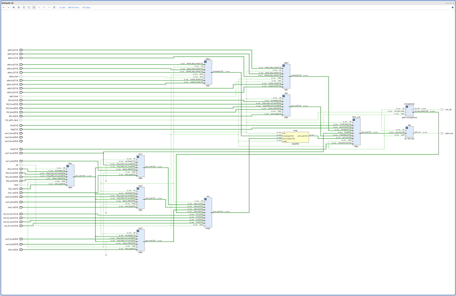
The following schematic is the result of the Vivado Elaborated Design after the RTL Analysis.
To set or read the status of the synth module, the C software application writes or reads to the registers of the Synth module.
Register map
The different registers controlled by the C application are grouped to save MiniZed resources.
The processor interacts with the Synth Module as follows:
- Generate (i.e., write) a pulse to start the amplifier envelope ADSR generation.
- Generate (i.e., write) a pulse to start the filter envelope ADSR generation.
- set (i.e., write) the value of the Oscillator 1 frequency carrier control word osc1_fccw
- set (i.e., write) the value of the Oscillator 1 frequency offset control word osc1_focw
- set (i.e., write) the value of the Oscillator 1 phase offset control word osc1_pho
- set (i.e., write) the value of the Oscillator 2 frequency carrier control word osc2_fccw
- set (i.e., write) the value of the Oscillator 2 frequency offset control word osc2_focw
- set (i.e., write) the value of the Oscillator 3 phase offset control word osc2_pho
- set (i.e., write) the value of the Oscillator 3 frequency carrier control word osc3_fccw
- set (i.e., write) the value of the Oscillator 3 frequency offset control word osc3_focw
- set (i.e., write) the value of the Oscillator 3 phase offset control word osc3_pho
- set (i.e., write) the value of the Oscillators Low-Frequency Oscillator (LFO) frequency carrier control word lfoo_fccw
- set (i.e., write) the value of the Oscillators Low-Frequency Oscillator (LFO) frequency offset control word lfoo_focw
- set (i.e., write) the value of the Oscillators Low-Frequency Oscillator (LFO) phase offset control word lfoo_pho
- set (i.e., write) the value of the Filter Low-Frequency Oscillator (LFO) frequency carrier control word lfof_fccw
- set (i.e., write) the value of the Filter Low-Frequency Oscillator (LFO) frequency offset control word lfof_focw
- set (i.e., write) the value of the Filter Low-Frequency Oscillator (LFO) phase offset control word lfof_pho
- set (i.e., write) the value of the Amplifier ADSR envelope generator configuration attack step adsra_a
- set (i.e., write) the value of the Amplifier ADSR envelope generator configuration decay step adsra_d
- set (i.e., write) the value of the Amplifier ADSR envelope generator configuration sustain level adsra_sl
- set (i.e., write) the value of the Amplifier ADSR envelope generator configuration, steps for the release segment, adsra_r
- set (i.e., write) the value of the Amplifier ADSR envelope generator configuration, time for the sustain segment, adsra_st
- set (i.e., write) the value of the Filter ADSR envelope generator configuration attack step adsrf_a
- set (i.e., write) the value of the Filter ADSR envelope generator configuration decay step adsrf_d
- set (i.e., write) the value of the Filter ADSR envelope generator configuration sustain level adsrf_sl
- set (i.e., write) the value of the Filter ADSR envelope generator configuration, steps for the release segment, adsrf_r
- set (i.e., write) the value of the Filter ADSR envelope generator configuration, time for the sustain segment, adsrf_st
- set (i.e., write) the value of the Filter cutoff frequency, fcut
- set (i.e., write) the value of the Filter resonance amount, fcres
- set (i.e., write) the value of the Filter resonance amount, fcres
- set (i.e., write) the value of the Filter Envelope Generator amount, fcres
- set (i.e., write) the wave type for the Oscillator 1, osc1_wt
- set (i.e., write) the wave type for the Oscillator 2, osc2_wt
- set (i.e., write) the wave type for the Oscillator 3, osc3_wt
- set (i.e., write) the wave type for the Oscillators Low-Frequency Oscillator (LFO), lfoo_wt
- set (i.e., write) the wave type for the Filter Low-Frequency Oscillator (LFO), lfoo_wt
- set (i.e., write) the mixer level, volume, for the Oscillator 1, mix_lvl_osc1
- set (i.e., write) the mixer level, volume, for the Oscillator 2, mix_lvl_osc2
- set (i.e., write) the mixer level, volume, for the Oscillator 3, mix_lvl_osc3
- set (i.e., write) the mixer level, volume, for the Microphone input mix_lvl_mic
- set (i.e., write) the maximum amount the Oscillators LFO moves the Oscillators pitch up and down
- set (i.e., write) sets the maximum amount the Filter LFO moves the Filter Cutoff up and down,
- check (i.e., read) the idle status and retrieve the envelope amplitude data
Write registers
- Register 0: Gates Register {30'b0, adsrf_start,adsra_start}
- bit 0: adsra_start, generate a pulse to start the oscillator envelope generation
- bit 1: adsrf_start, generate a pulse to start the filter envelope generation
- Register 1:osc1_fccw
- bits 29 to 0: osc1_fccw 30-bits Pitch, oscillator 1 frequency carrier ctrl word
- Register 2 :osc1_focw
- bits 29 to 0: osc1_focw 30-bits Detune, oscillator 1 frequency offset ctrl word
- Register 3: osc1_pho:
- bits 29 to 0: osc1_pho, Phase shift, oscillator 1 phase offset ctrl word
- Register 4 :osc2_fccw:
- bits 29 to 0: osc2_fccw 30-bits Pitch, oscillator 2 frequency carrier ctrl word
- Register 5 :osc2_focw
- bits 29 to 0: osc2_focw 30-bits Detune, oscillator 2 frequency offset ctrl word
- Register 6: osc2_pho
- bits 29 to 0: osc2_pho, Phase shift, oscillator 2 phase offset ctrl word
- Register 7:osc3_fccw
- bits 29 to 0: osc3_fccw 30-bits Pitch, oscillator 3 frequency carrier ctrl word
- Register 8 :osc3_focw
- bits 29 to 0: osc3_focw 30-bits Detune, oscillator 3 frequency offset ctrl word
- Register 9: osc3_pho
- bits 29 to 0: osc3_pho, Phase shift, oscillator 3 phase offset ctrl word
- Register 10:lfoo_fccw
- bits 29 to 0: lfoo_fccw 30-bits Pitch, LFO oscillator frequency carrier ctrl word
- Register 11 :lfoo_focw
- bits 29 to 0: lfoo_focw 30-bits Detune, LFO oscillator frequency offset ctrl word
- Register 12: lfoo_pho
- bits 29 to 0: lfoo_pho, Phase shift, LFO oscillator phase offset ctrl word
- Register 13:lfof_fccw
- bits 29 to 0: lfof_fccw 30-bits Pitch, LFO filter frequency carrier ctrl word
- Register 14:lfof_focw
- bits 29 to 0: lfof_focw 30-bits Detune, LFO filter frequency offset ctrl word
- Register 15: lfof_pho
- bits 29 to 0: lfof_pho, Phase shift, LFO filter phase offset ctrl word
- Register 16: adsra_a, Amplifier ADSR configuration attack step
- bits 31 to 0: adsra_a, precalculated (Amax - 0)/(t_attack - t_sys) steps for the attack segment
- Register 17: adsra_d, Amplifier ADSR configuration decay step
- bits 31 to 0: adsra_d, precalculated (A_max-A_sus) / (t_sustain / t_sys) steps for the decay segment
- Register 18: adsra_sl, Amplifier ADSR configuration sustain level
- bits 31 to 0: adsra_sl, amplitude for the sustain segment
- Register 19: adsra_r, Amplifier ADSR configuration, steps for the release segment
- bits 31 to 0: adsra_r, precalculated (A_sus - 0)/(t_release - t_sys) steps for the release segment
- Register 20: adsra_st, Amplifier ADSR configuration, time for the sustain segment
- bits 31 to 0: adsra_st, tsustain / t_sys steps for the sustain
- Register 21: adsrf_a, Filter ADSR configuration attack step
- bits 31 to 0: adsrf_a, precalculated (Amax - 0)/(t_attack - t_sys) steps for the attack segment
- Register 22: adsrf_d, Filter ADSR configuration decay step
- bits 31 to 0: adsrf_d, precalculated (A_max-A_sus) / (t_sustain / t_sys) steps for the decay segment
- Register 23: adsrf_sl, Filter ADSR configuration sustain level
- bits 31 to 0: adsrf_sl, amplitude for the sustain segment
- Register 24: adsrf_r, Filter ADSR configuration, steps for the release segment
- bits 31 to 0: adsrf_r, precalculated (A_sus - 0)/(t_release - t_sys) steps for the release segment
- Register 25: adsrf_st, Filter ADSR configuration, time for the sustain segment
- bits 31 to 0: adsrf_st, tsustain / t_sys steps for the sustain
- Register 26: fcut filter cutoff frequency
- bits 31 to 0: fcut, filter cutoff frequency
- Register 27: fres, filter resonance level
- bits 31 to 0: fres, filter resonance level
- Register 28: feg, filter envelope generator amount
- bits 31 to 0: feg, filter envelope generator amount
- Register 29: wave types:
- bits 2 to 0: osc1_wt, oscillator 1 wave type
- bits 5 to 3: osc2_wt, oscillator 2 wave type
- bits 8 to 6: osc3_wt, oscillator 3 wave type
- bits 11 to 9: lfoo_wt, LFO oscillator wave type
- bits 14 to 12: lfof_wt, LFO filter wave type
- Register 30: Mix levels osc1 & osc2
- bits 15 to 0: mix_lvl_osc1, oscillator 1 volume level
- bits 31 to 16: mix_lvl_osc2, oscillator 2 volume level
- Register 31: Mix levels osc3 & mic
- bits 15 to 0: mix_lvl_osc3, oscillator 3 volume level
- bits 31 to 16: mix_lvl_mic, mic volume level
- Register 32: LFO amounts configurations
- bits 15 to 0: lfoo_lvl, Sets the maximum amount the LFO moves the oscillator pitch up and down, up to +/- 1 octave.
- bits 31 to 16: lfof_lvl, Sets the maximum amount the LFO moves the Filter Cutoff up and down, up to +/- 5 octaves.
Read Registers
- Register 33: idle status and amplifier envelope amplitude data
- bits 31 to 16: 16-bit envelope data
- bit 0: idle status
Creation of a new AXI4 Peripheral IP
Based on the previous configuration a a new AXI4 Peripheral IP is created with the Vivado IP Packager
| {gallery}New AXI4 Peripheral |
|---|
|
Create and package new IP: Create a new AXI4 Peripheral |
|
Add Interfaces: Configure 34 registers |

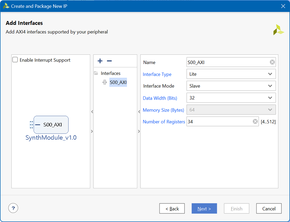
User ports
- Input external P1-bit DM MiniZed Signal AUDIO_DAT
- 1-bit PDM sound output
- generated microphone clock signal route to Minized external AUDIO_CLK
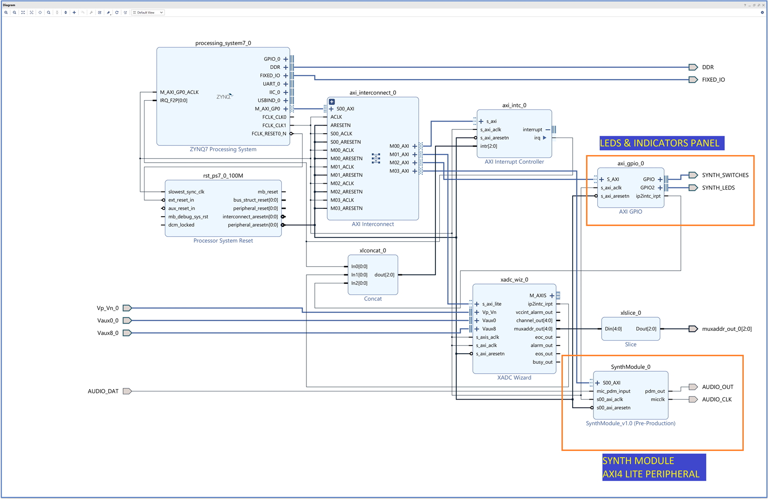
All the files used by the Synth Module IP are added to the project and modified if needed.

IP project files
| File | Type |
| hdl/SynthModule_v1_0_S00_AXI.v | verilogSource |
| src/adsr.sv | systemVerilogSource |
| src/amplifier.sv | systemVerilogSource |
| src/ddfs.sv | systemVerilogSource |
| src/ds_1bit_dac.sv | systemVerilogSource |
| src/filter.sv | systemVerilogSource |
| src/lfsr.sv | systemVerilogSource |
| src/mixer.sv | systemVerilogSource |
| src/pdm_clk_gen.sv | systemVerilogSource |
| src/pdm_microphone.sv | systemVerilogSource |
| src/saw_tooth.sv | systemVerilogSource |
| src/sin_rom.sv | systemVerilogSource |
| src/square_wave.sv | systemVerilogSource |
| src/synth_module.sv | systemVerilogSource |
| src/triangle_wave.sv | systemVerilogSource |
| src/sin_table.mem | mem |
| hdl/SynthModule_v1_0.v | verilogSource |
Standalone C Driver
To facilitate communication with the Synthesizer Module, a C driver has been developed so that the C application does not have to worry about the implementation details of the modules in HDL.
The drivers are also included in the IP module project so that they are included in the .xsa file that Vivado will export when we export the hardware definition for use with the VITIS integrated development environment (IDE).
Driver header file
#ifndef SYNTHMODULE1_H
#define SYNTHMODULE1_H


/****************** Include Files ********************/
#include <stdio.h>
#include "xil_types.h"
#include "xstatus.h"
#include "xil_exception.h"
#include "xil_printf.h"
#include "xil_io.h"


#define PHA_WIDTH 30 // bits in DDFS phase register
#define SYS_CLK_FREQ 100
// MAX is 0x80000000
#define SYNTHMODULE1_MAX            0x7fffffff
#define SYNTHMODULE1_BYPASS_PATTERN 0xffffffff
#define SYNTHMODULE1_STOP_PATTERN   0x00000000

#define SINE     0x00
#define SQUARE   0x01
#define SAW      0x02
#define TRIANGLE 0x03
#define NOISE    0x04

#define SYNTHMODULE_S00_AXI_SLV_REG0_OFFSET 0
#define SYNTHMODULE_S00_AXI_SLV_REG1_OFFSET 4
#define SYNTHMODULE_S00_AXI_SLV_REG2_OFFSET 8
#define SYNTHMODULE_S00_AXI_SLV_REG3_OFFSET 12
#define SYNTHMODULE_S00_AXI_SLV_REG4_OFFSET 16
#define SYNTHMODULE_S00_AXI_SLV_REG5_OFFSET 20
#define SYNTHMODULE_S00_AXI_SLV_REG6_OFFSET 24
#define SYNTHMODULE_S00_AXI_SLV_REG7_OFFSET 28
#define SYNTHMODULE_S00_AXI_SLV_REG8_OFFSET 32
#define SYNTHMODULE_S00_AXI_SLV_REG9_OFFSET 36
#define SYNTHMODULE_S00_AXI_SLV_REG10_OFFSET 40
#define SYNTHMODULE_S00_AXI_SLV_REG11_OFFSET 44
#define SYNTHMODULE_S00_AXI_SLV_REG12_OFFSET 48
#define SYNTHMODULE_S00_AXI_SLV_REG13_OFFSET 52
#define SYNTHMODULE_S00_AXI_SLV_REG14_OFFSET 56
#define SYNTHMODULE_S00_AXI_SLV_REG15_OFFSET 60
#define SYNTHMODULE_S00_AXI_SLV_REG16_OFFSET 64
#define SYNTHMODULE_S00_AXI_SLV_REG17_OFFSET 68
#define SYNTHMODULE_S00_AXI_SLV_REG18_OFFSET 72
#define SYNTHMODULE_S00_AXI_SLV_REG19_OFFSET 76
#define SYNTHMODULE_S00_AXI_SLV_REG20_OFFSET 80
#define SYNTHMODULE_S00_AXI_SLV_REG21_OFFSET 84
#define SYNTHMODULE_S00_AXI_SLV_REG22_OFFSET 88
#define SYNTHMODULE_S00_AXI_SLV_REG23_OFFSET 92
#define SYNTHMODULE_S00_AXI_SLV_REG24_OFFSET 96
#define SYNTHMODULE_S00_AXI_SLV_REG25_OFFSET 100
#define SYNTHMODULE_S00_AXI_SLV_REG26_OFFSET 104
#define SYNTHMODULE_S00_AXI_SLV_REG27_OFFSET 108
#define SYNTHMODULE_S00_AXI_SLV_REG28_OFFSET 112
#define SYNTHMODULE_S00_AXI_SLV_REG29_OFFSET 116
#define SYNTHMODULE_S00_AXI_SLV_REG30_OFFSET 120
#define SYNTHMODULE_S00_AXI_SLV_REG31_OFFSET 124
#define SYNTHMODULE_S00_AXI_SLV_REG32_OFFSET 128
#define SYNTHMODULE_S00_AXI_SLV_REG33_OFFSET 132

/**
* Register 0: Gates Register {30'b0, adsrf_start,adsra_start}
* bit 0: adsra_start, generate a pulse to start the oscillator envelope generation
* bit 1: adsrf_start, generate a pulse to start the filter envelope generation
*/
#define ADSR_START_GATES_OFFSET  SYNTHMODULE_S00_AXI_SLV_REG0_OFFSET

/**
* Register 1 :osc1_fccw
* bits 29 to 0: osc1_fccw 30-bits Pitch, oscillator 1 frequency carrier ctrl word
*/
#define OSC1_FCCW_OFFSET 	     SYNTHMODULE_S00_AXI_SLV_REG1_OFFSET

/**
* Register 2 :osc1_focw
* bits 29 to 0: osc1_focw 30-bits Detune, oscillator 1 frequency offset ctrl word
*/
#define OSC1_FOCW_OFFSET 	     SYNTHMODULE_S00_AXI_SLV_REG2_OFFSET

/**
* Register 3: osc1_pho:
* bits 29 to 0: osc1_pho, Phase shift, oscillator 1 phase offset ctrl word
*/
#define OSC1_PHO_OFFSET 	     SYNTHMODULE_S00_AXI_SLV_REG3_OFFSET

/**
* Register 4 :osc2_fccw:
* bits 29 to 0: osc2_fccw 30-bits Pitch, oscillator 2 frequency carrier ctrl word
*/
#define OSC2_FCCW_OFFSET 	     SYNTHMODULE_S00_AXI_SLV_REG4_OFFSET

/**
* Register 5 :osc2_focw
* bits 29 to 0: osc2_focw 30-bits Detune, oscillator 2 frequency offset ctrl word
*/
#define OSC2_FOCW_OFFSET 	     SYNTHMODULE_S00_AXI_SLV_REG5_OFFSET

/**
* Register 6: osc2_pho
* bits 29 to 0: osc2_pho, Phase shift, oscillator 2 phase offset ctrl word
*/
#define OSC2_PHO_OFFSET 	     SYNTHMODULE_S00_AXI_SLV_REG6_OFFSET

/**
* Register 7 :osc3_fccw
* bits 29 to 0: osc3_fccw 30-bits Pitch, oscillator 3 frequency carrier ctrl word
*/
#define OSC3_FCCW_OFFSET 	     SYNTHMODULE_S00_AXI_SLV_REG7_OFFSET

/**
* Register 8 :osc3_focw
* bits 29 to 0: osc3_focw 30-bits Detune, oscillator 3 frequency offset ctrl word
*/
#define OSC3_FOCW_OFFSET 	     SYNTHMODULE_S00_AXI_SLV_REG8_OFFSET

/**
* Register 9: osc3_pho
* bits 29 to 0: osc3_pho, Phase shift, oscillator 3 phase offset ctrl word
*/
#define OSC3_PHO_OFFSET 	     SYNTHMODULE_S00_AXI_SLV_REG9_OFFSET

/**
* Register 10 :lfoo_fccw
* bits 29 to 0: lfoo_fccw 30-bits Pitch, LFO oscillator frequency carrier ctrl word
*/
#define LFOO_FCCW_OFFSET 	     SYNTHMODULE_S00_AXI_SLV_REG10_OFFSET

/**
* Register 11 :lfoo_focw
* bits 29 to 0: lfoo_focw 30-bits Detune, LFO oscillator frequency offset ctrl word
*/
#define LFOO_FOCW_OFFSET 	     SYNTHMODULE_S00_AXI_SLV_REG11_OFFSET

/**
* Register 12: lfoo_pho
* bits 29 to 0: lfoo_pho, Phase shift, LFO oscillator phase offset ctrl word
*/
#define LFOO_PHO_OFFSET 	     SYNTHMODULE_S00_AXI_SLV_REG12_OFFSET

/**
* Register 13 :lfof_fccw
* bits 29 to 0: lfof_fccw 30-bits Pitch, LFO filter frequency carrier ctrl word
*/
#define LFOF_FCCW_OFFSET 	     SYNTHMODULE_S00_AXI_SLV_REG13_OFFSET

/**
* Register 14 :lfof_focw
* bits 29 to 0: lfof_focw 30-bits Detune, LFO filter frequency offset ctrl word
*/
#define LFOF_FOCW_OFFSET 	     SYNTHMODULE_S00_AXI_SLV_REG14_OFFSET

/**
* Register 15: lfof_pho
* bits 29 to 0: lfof_pho, Phase shift, LFO filter phase offset ctrl word
*/
#define LFOF_PHO_OFFSET 	     SYNTHMODULE_S00_AXI_SLV_REG15_OFFSET

/**
* Register 16: adsra_a, Amplifier ADSR configuration attack step
* bits 31 to 0: adsra_a, precalculated (Amax - 0)/(t_attack - t_sys) steps for the attack segment
*/
#define ADSRA_A_OFFSET 	         SYNTHMODULE_S00_AXI_SLV_REG16_OFFSET

/**
* Register 17: adsra_d, Amplifier ADSR configuration decay step
* bits 31 to 0: adsra_d, precalculated (A_max-A_sus) / (t_sustain / t_sys) steps for the decay segment
*/
#define ADSRA_D_OFFSET 	         SYNTHMODULE_S00_AXI_SLV_REG17_OFFSET

/**
* Register 18: adsra_sl, Amplifier ADSR configuration sustain level
* bits 31 to 0: adsra_sl, amplitude for the sustain segment
*/
#define ADSRA_SL_OFFSET 	     SYNTHMODULE_S00_AXI_SLV_REG18_OFFSET

/**
* Register 19: adsra_r, Amplifier ADSR configuration, steps for the release segment
* bits 31 to 0: adsra_r, precalculated (A_sus - 0)/(t_release - t_sys) steps fot the release segment
*/
#define ADSRA_R_OFFSET 	         SYNTHMODULE_S00_AXI_SLV_REG19_OFFSET

/**
* Register 20: adsra_st, Amplifier ADSR configuration, time for the sustain segment
* bits 31 to 0: adsra_st, tsustain / t_sys steps for the sustain
*/
#define ADSRA_ST_OFFSET 	     SYNTHMODULE_S00_AXI_SLV_REG20_OFFSET

/**
* Register 21: adsrf_a, Filter ADSR configuration attack step
* bits 31 to 0: adsrf_a, precalculated (Amax - 0)/(t_attack - t_sys) steps for the attack segment
*/
#define ADSRF_A_OFFSET 	         SYNTHMODULE_S00_AXI_SLV_REG21_OFFSET

/**
* Register 22: adsrf_d, Filter ADSR configuration decay step
* bits 31 to 0: adsrf_d, precalculated (A_max-A_sus) / (t_sustain / t_sys) steps for the decay segment
*/
#define ADSRF_D_OFFSET 	         SYNTHMODULE_S00_AXI_SLV_REG22_OFFSET

/**
* Register 23: adsrf_sl, Filter ADSR configuration sustain level
* bits 31 to 0: adsrf_sl, amplitude for the sustain segment
*/
#define ADSRF_SL_OFFSET 	     SYNTHMODULE_S00_AXI_SLV_REG23_OFFSET

/**
* Register 24: adsrf_r, Filter ADSR configuration, steps for the release segment
* bits 31 to 0: adsrf_r, precalculated (A_sus - 0)/(t_release - t_sys) steps for the release segment
*/
#define ADSRF_R_OFFSET 	         SYNTHMODULE_S00_AXI_SLV_REG24_OFFSET

/**
* Register 25: adsrf_st, Filter ADSR configuration, time for the sustain segment
* bits 31 to 0: adsrf_st, tsustain / t_sys steps for the sustain
*/
#define ADSRF_ST_OFFSET 	     SYNTHMODULE_S00_AXI_SLV_REG25_OFFSET

/**
* Register 26: fcut filter cutoff frequency
* bits 31 to 0: fcut, filter cutoff frequency
*/
#define FCUT_OFFSET 	         SYNTHMODULE_S00_AXI_SLV_REG26_OFFSET

/**
* Register 27: fres, filter resonance level
* bits 31 to 0: fres, filter resonance level
*/
#define FRES_OFFSET 	         SYNTHMODULE_S00_AXI_SLV_REG27_OFFSET

/**
* Register 28: feg, filter envelope generator amount
* bits 31 to 0: feg, filter envelope generator amount
*/
#define FEG_OFFSET 	             SYNTHMODULE_S00_AXI_SLV_REG28_OFFSET

/**
* Register 29: wave_types:
* bits 2 to 0: osc1_wt, oscillator 1 wave type
* bits 5 to 3: osc2_wt, oscillator 2 wave type
* bits 8 to 6: osc3_wt, oscillator 3 wave type
* bits 11 to 9: lfoo_wt, LFO oscillator wave type
* bits 14 to 12: lfof_wt, LFO filter wave type
*/
#define WAVE_TYPES_OFFSET 	     SYNTHMODULE_S00_AXI_SLV_REG29_OFFSET


/**
* Register 30: Mix_levels_osc1_osc2
* bits 15 to 0: mix_lvl_osc1, oscillator 1 volume level
* bits 31 to 16: mix_lvl_osc2, oscillator 2 volume level
*/
#define MIX_LVL_OSC1_OSC2_OFFSET SYNTHMODULE_S00_AXI_SLV_REG30_OFFSET

/**
* Register 31: Mix_levels_osc3_mic
* bits 15 to 0: mix_lvl_osc3, oscillator 3 volume level
* bits 31 to 16: mix_lvl_mic, mic volume level
*/
#define MIX_LVL_OSC3_MIC_OFFSET  SYNTHMODULE_S00_AXI_SLV_REG31_OFFSET

/**
* Register 32: LFO amounts configurations
* bits 15 to 0: lfoo_lvl, Sets the maximum amount the LFO moves the Oscillators pitch up and down, up to +/- 1 octave.
* bits 31 to 16: lfof_lvl, Sets the maximum amount the LFO moves the Filter Cutoff up and down, up to +/- 5 octaves.
*/
#define LFO_AMOUNTS_OFFSET 	     SYNTHMODULE_S00_AXI_SLV_REG32_OFFSET

/**
* Read Registers
* Register 33: idle status and amplifier envelope amplitude data
* bits 31 to 16: 16 bit envelope data
* bit 0: idle status
*/
#define AMP_ADSR_STATUS_OFFSET 	 SYNTHMODULE_S00_AXI_SLV_REG33_OFFSET


/**
* Register 1 :osc1_fccw
* bits 29 to 0: osc1_fccw 30-bits Pitch, oscillator 1 frequency carrier ctrl word
*/
#define OSC1_FCCW_OFFSET 	     SYNTHMODULE_S00_AXI_SLV_REG1_OFFSET

/**
* Register 2 :osc1_focw
* bits 29 to 0: osc1_focw 30-bits Detune, oscillator 1 frequency offset ctrl word
*/
#define OSC1_FOCW_OFFSET 	     SYNTHMODULE_S00_AXI_SLV_REG2_OFFSET

/**
* Register 3: osc1_pho:
* bits 29 to 0: osc1_pho, Phase shift, oscillator 1 phase offset ctrl word
*/
#define OSC1_PHO_OFFSET 	     SYNTHMODULE_S00_AXI_SLV_REG3_OFFSET


typedef struct OscillatorConfig {
   u32 fccwOffset;
   int fccw;  // Pitch, oscillator frequency carrier ctrl word

   u32 focwOffset;
   int focw;  // Detune, oscillator frequency offset ctrl word

   u32 phoOffset;
   int pho;  // Phase shift, oscillator phase offset ctrl word

   u32 waveTypeOffset; //
   u8  waveTypeIndex;
   u8  waveType;

   u32 amplitudeOffset;
   u8  amplitudeIndex;
   // mix level
   float amplitude;
} OscillatorConfig;

typedef struct AdsrConfig {
	u32 atackStepsOffset;
	u32 ams;

	u32 decayStepsOffset;
	u32 dms;

	u32 sustainLevelOffset;
	float slevel;

	u32 sustainTimeOffset;
	u32 sms;

	u32 releaseStepsOffset;
	u32 rms;

	u32 gateOffset;

	u32 statusOffset;
	u32 status;
} AdsrConfig;

typedef struct MicConfig {
	u32 micLevelOffset;
	u32 amplitudeIndex;
	float amplitude;
} MicConfig;

typedef struct Synth{
	u32 			 baseAddr;
	OscillatorConfig osc_1;
	OscillatorConfig osc_2;
	OscillatorConfig osc_3;
	OscillatorConfig osc_lfo;
	OscillatorConfig filter_lfo;
    MicConfig        mic;
	AdsrConfig       amplifier_adsr;
	AdsrConfig       filter_adsr;
} Synth;


/**************************** Type Definitions *****************************/
/**
 *
 * Write a value to a SYNTHMODULE register. A 32 bit write is performed.
 * If the component is implemented in a smaller width, only the least
 * significant data is written.
 *
 * @param   BaseAddress is the base address of the SYNTHMODULEdevice.
 * @param   RegOffset is the register offset from the base to write to.
 * @param   Data is the data written to the register.
 *
 * @return  None.
 *
 * @note
 * C-style signature:
 * 	void SYNTHMODULE_mWriteReg(u32 BaseAddress, unsigned RegOffset, u32 Data)
 *
 */
#define SYNTHMODULE_mWriteReg(BaseAddress, RegOffset, Data) \
  	Xil_Out32((BaseAddress) + (RegOffset), (u32)(Data))

/**
 *
 * Read a value from a SYNTHMODULE register. A 32 bit read is performed.
 * If the component is implemented in a smaller width, only the least
 * significant data is read from the register. The most significant data
 * will be read as 0.
 *
 * @param   BaseAddress is the base address of the SYNTHMODULE device.
 * @param   RegOffset is the register offset from the base to write to.
 *
 * @return  Data is the data from the register.
 *
 * @note
 * C-style signature:
 * 	u32 SYNTHMODULE_mReadReg(u32 BaseAddress, unsigned RegOffset)
 *
 */
#define SYNTHMODULE_mReadReg(BaseAddress, RegOffset) \
    Xil_In32((BaseAddress) + (RegOffset))


/************************** Function Prototypes ****************************/
/**
 *
 * Run a self-test on the driver/device. Note this may be a destructive test if
 * resets of the device are performed.
 *
 * If the hardware system is not built correctly, this function may never
 * return to the caller.
 *
 * @param   baseaddr_p is the base address of the SYNTHMODULE instance to be worked on.
 *
 * @return
 *
 *    - XST_SUCCESS   if all self-test code passed
 *    - XST_FAILURE   if any self-test code failed
 *
 * @note    Caching must be turned off for this function to work.
 * @note    Self test may fail if data memory and device are not on the same bus.
 *
 */
XStatus SYNTHMODULE1_Reg_SelfTest(u32 baseaddr_p);


void SYNTHMODULE1_init(Synth * synth, u32 baseAddr);

void SYNTHMODULE1_osc1_set_carrier_freq(Synth * synth, int freq);
void SYNTHMODULE1_osc1_set_offset_freq(Synth * synth, int freq);
void SYNTHMODULE1_osc1_set_phase_degree(Synth * synth, int phase);
void SYNTHMODULE1_osc1_set_amp(Synth * synth, float amp);
void SYNTHMODULE1_osc1_set_wave_type(Synth * synth, int waveType);

void SYNTHMODULE1_osc2_set_carrier_freq(Synth * synth, int freq);
void SYNTHMODULE1_osc2_set_offset_freq(Synth * synth, int freq);
void SYNTHMODULE1_osc2_set_phase_degree(Synth * synth, int phase);
void SYNTHMODULE1_osc2_set_amp(Synth * synth, float amp);
void SYNTHMODULE1_osc2_set_wave_type(Synth * synth, int waveType);

void SYNTHMODULE1_osc3_set_carrier_freq(Synth * synth, int freq);
void SYNTHMODULE1_osc3_set_offset_freq(Synth * synth, int freq);
void SYNTHMODULE1_osc3_set_phase_degree(Synth * synth, int phase);
void SYNTHMODULE1_osc3_set_amp(Synth * synth, float amp);
void SYNTHMODULE1_osc3_set_wave_type(Synth * synth, int waveType);

void SYNTHMODULE1_lfoo_set_carrier_freq(Synth * synth, int freq);
void SYNTHMODULE1_lfoo_set_offset_freq(Synth * synth, int freq);
void SYNTHMODULE1_lfoo_set_phase_degree(Synth * synth, int phase);
void SYNTHMODULE1_lfoo_set_amp(Synth * synth, float amp);
void SYNTHMODULE1_lfoo_set_wave_type(Synth * synth, int waveType);

void SYNTHMODULE1_lfof_set_carrier_freq(Synth * synth, int freq);
void SYNTHMODULE1_lfof_set_offset_freq(Synth * synth, int freq);
void SYNTHMODULE1_lfof_set_phase_degree(Synth * synth, int phase);
void SYNTHMODULE1_lfof_set_amp(Synth * synth, float amp);
void SYNTHMODULE1_lfof_set_wave_type(Synth * synth, int waveType);


int SYNTHMODULE1_amplifier_adsr_idle(Synth * synth);
void SYNTHMODULE1_amplifier_adsr_start(Synth * synth);
void SYNTHMODULE1_amplifier_adsr_abort(Synth * synth);
void SYNTHMODULE1_amplifier_adsr_bypass(Synth * synth);
void SYNTHMODULE1_amplifier_adsr_set_env(Synth * synth, int attack_ms, int decay_ms, int sustain_ms, int release_ms, float sus_level);
void SYNTHMODULE1_amplifier_adsr_select_env(Synth * synth, int n);

int SYNTHMODULE1_filter_adsr_idle(Synth * synth);
void SYNTHMODULE1_filter_adsr_start(Synth * synth);
void SYNTHMODULE1_filter_adsr_abort(Synth * synth);
void SYNTHMODULE1_filter_adsr_bypass(Synth * synth);
void SYNTHMODULE1_filter_adsr_set_env(Synth * synth, int attack_ms, int decay_ms, int sustain_ms, int release_ms, float sus_level);
void SYNTHMODULE1_filter_adsr_select_env(Synth * synth, int n);

void SYNTHMODULE1_amplifier_adsr_write_reg(Synth * synth);

int SYNTHMODULE1_calc_note_freq(int octave, int noteIndex);
void SYNTHMODULE1_play_note(Synth * synth, int note, int octave, int duration);

u32 SYNTHMODULE1_calc_phase_control_word(int phase);

u32 SYNTHMODULE1_convert_amp_to_q214(float amp) ;

void SYNTHMODULE1_set_wave_types(Synth* synth);

void SYNTHMODULE1_set_mix_lvl_osc1_osc2(Synth* synth);


void SYNTHMODULE1_set_mix_lvl_osc3_mic(Synth* synth);

u32 SYNTHMODULE1_calc_lfo_freq_control_word(float freq);

void SYNTHMODULE1_mic_set_amp(Synth* synth, float amp);

void setBaseConfiguration(Synth * synth);


#endif // SYNTHMODULE1_H
Driver Implementation:
/***************************** Include Files *******************************/
#include "SynthModule1.h"

/************************** Function Definitions ***************************/

/************************** Constant Definitions ***************************/
#define READ_WRITE_MUL_FACTOR 0x10


/**
 *
 * Initialize the modulecalculates write and read register addresses
 * based on SynthModule base address. SYNTHMODULE1_init() must be call once
 * before any other API call
 *
 * @param   baseAddr is the base address of the SYNTHMODULE instance to be worked on.
 *
 * @return
 *
 *    - void
 *
 */
void SYNTHMODULE1_init(Synth * synth, u32 baseAddr) {

	synth->baseAddr = baseAddr;

	// calculate oscillator 1 write register addresses
   synth->osc_1.fccwOffset       =  OSC1_FCCW_OFFSET;
   synth->osc_1.focwOffset       =  OSC1_FOCW_OFFSET;
   synth->osc_1.phoOffset        =  OSC1_PHO_OFFSET;
   synth->osc_1.waveTypeOffset   =  WAVE_TYPES_OFFSET;
   synth->osc_1.waveTypeIndex  = 0;
   synth->osc_1.amplitudeOffset  =  MIX_LVL_OSC1_OSC2_OFFSET;
   synth->osc_1.amplitudeIndex = 0;

   // calculate oscillator 2 write register addresses
   synth->osc_2.fccwOffset       =  OSC2_FCCW_OFFSET;
   synth->osc_2.focwOffset       =  OSC2_FOCW_OFFSET;
   synth->osc_2.phoOffset        =  OSC2_PHO_OFFSET;
   synth->osc_2.waveTypeOffset   =  WAVE_TYPES_OFFSET;
   synth->osc_2.waveTypeIndex  = 1;
   synth->osc_2.amplitudeOffset  =  MIX_LVL_OSC1_OSC2_OFFSET;
   synth->osc_2.amplitudeIndex = 1;

   // calculate oscillator 3 write register addresses
   synth->osc_3.fccwOffset       =  OSC3_FCCW_OFFSET;
   synth->osc_3.focwOffset       =  OSC3_FOCW_OFFSET;
   synth->osc_3.phoOffset        =  OSC3_PHO_OFFSET;
   synth->osc_3.waveTypeOffset   =  WAVE_TYPES_OFFSET;
   synth->osc_3.waveTypeIndex  = 2;
   synth->osc_3.amplitudeOffset  =  MIX_LVL_OSC3_MIC_OFFSET;
   synth->osc_3.amplitudeIndex = 0;

   // calculate oscillators lfo write register addresses
   synth->osc_lfo.fccwOffset       =  LFOO_FCCW_OFFSET;
   synth->osc_lfo.focwOffset       =  LFOO_FOCW_OFFSET;
   synth->osc_lfo.phoOffset        =  LFOO_PHO_OFFSET;
   synth->osc_lfo.waveTypeOffset   =  WAVE_TYPES_OFFSET;
   synth->osc_lfo.waveTypeIndex  = 3;
   synth->osc_lfo.amplitudeOffset  =  LFO_AMOUNTS_OFFSET;
   synth->osc_lfo.amplitudeIndex = 0;

   // calculate filter lfo write register addresses
   synth->filter_lfo.fccwOffset       =  LFOF_FCCW_OFFSET;
   synth->filter_lfo.focwOffset       =  LFOF_FOCW_OFFSET;
   synth->filter_lfo.phoOffset        =  LFOF_PHO_OFFSET;
   synth->filter_lfo.waveTypeOffset   =  WAVE_TYPES_OFFSET;
   synth->filter_lfo.waveTypeIndex  = 4;
   synth->filter_lfo.amplitudeOffset  =  LFO_AMOUNTS_OFFSET;
   synth->filter_lfo.amplitudeIndex = 1;

   // calculate microphone write register addresses
   synth->mic.micLevelOffset          =  MIX_LVL_OSC3_MIC_OFFSET;
   synth->mic.amplitudeIndex        = 1;

   // calculate amplifier adsr write register addresses
   synth->amplifier_adsr.atackStepsOffset   =  ADSRA_A_OFFSET;
   synth->amplifier_adsr.decayStepsOffset   =  ADSRA_D_OFFSET;
   synth->amplifier_adsr.sustainLevelOffset =  ADSRA_SL_OFFSET;
   synth->amplifier_adsr.sustainTimeOffset  =  ADSRA_ST_OFFSET;
   synth->amplifier_adsr.releaseStepsOffset =  ADSRA_R_OFFSET;

   // calculate filter adsr write register addresses
   synth->filter_adsr.atackStepsOffset   =  ADSRF_A_OFFSET;
   synth->filter_adsr.decayStepsOffset   =  ADSRF_D_OFFSET;
   synth->filter_adsr.sustainLevelOffset =  ADSRF_SL_OFFSET;
   synth->filter_adsr.sustainTimeOffset  =  ADSRF_ST_OFFSET;
   synth->filter_adsr.releaseStepsOffset =  ADSRF_R_OFFSET;

   // calculate amplifier gate addresses
   synth->amplifier_adsr.gateOffset =  ADSR_START_GATES_OFFSET;

   // calculate amplifier adsr read register address
   synth->amplifier_adsr.statusOffset =  AMP_ADSR_STATUS_OFFSET;


}

/**
 * Configure System as:
 * 	- two main sawtooth wave oscillators
 * 	- two sinusoidal waves lfo
 * 	- 1 noise input
 * 	- 1 microphone input
 *
 *
 */
void setBaseConfiguration(Synth * synth) {

	SYNTHMODULE1_osc1_set_carrier_freq(synth, 262);
	SYNTHMODULE1_osc1_set_amp(synth, 0.9);
	SYNTHMODULE1_osc1_set_phase_degree(synth, 0);
	SYNTHMODULE1_osc1_set_wave_type(synth, SINE);

	SYNTHMODULE1_amplifier_adsr_bypass(synth);

	SYNTHMODULE1_osc2_set_carrier_freq(synth, 262);
	SYNTHMODULE1_osc2_set_wave_type(synth, SAW);

	SYNTHMODULE1_osc3_set_wave_type(synth, NOISE);
	SYNTHMODULE1_osc2_set_amp(synth, 0.0);
	SYNTHMODULE1_osc3_set_amp(synth, 0.0);
	SYNTHMODULE1_mic_set_amp(synth, 0.0);


	SYNTHMODULE1_lfoo_set_amp(synth, 0.0);
	SYNTHMODULE1_lfof_set_amp(synth, 0.0);

	SYNTHMODULE1_amplifier_adsr_set_env(synth, 100, 50, 100, 50, 0.9);

	SYNTHMODULE1_amplifier_adsr_start(synth);


}

/************************** Function Definitions ***************************/


/**************************  Support functions ***************************/

/**
 * Calculates frequency control word in steps
 * Only for audio frequencies above 10 Hz
 *
 * @param freq frequency in hertz
 */
u32 SYNTHMODULE1_calc_freq_control_word(int freq) {
	u32 fcw, p2n;
	float tmp;
	p2n = 1 << PHA_WIDTH;
	tmp = ((float) p2n) / (float) (SYS_CLK_FREQ * 1000000.0);
	fcw = (u32) (freq * tmp);
	return fcw;
}

/**
 * Calculate the frequency for lfo oscillators
 * lfo range is from 0.1Hz to 100Hz.
 *
 * @param freq frequency in hertz
 */
u32 SYNTHMODULE1_calc_lfo_freq_control_word(float freq) {
	u32 fcw, p2n;
	float tmp;
	p2n = 1 << PHA_WIDTH;
	tmp = ((float) p2n) / (float) (SYS_CLK_FREQ * 1000000.0);
	fcw = (u32) (freq * tmp);
	return fcw;
}

u32 SYNTHMODULE1_calc_phase_control_word(int phase) {
	u32 pha;
	pha = (SYS_CLK_FREQ * 1000000) * phase / 360;
	return pha;
}

u32 SYNTHMODULE1_convert_amp_to_q214(float amp) {
	// convert floating point to fixed-point Q2.14 format
	u32 q214;
	float max_amp;
	max_amp = (float) (0x4000); // amp * 2^15
	q214 = (u32) (amp * max_amp);

	return q214 & 0x0000ffff;
}

/**********************************************************
 * Setters
 **********************************************************/

/*********************************************************
 * Oscillator 1 setters
 *********************************************************/

void SYNTHMODULE1_osc1_set_carrier_freq(Synth * synth, int freq) {
	synth->osc_1.fccw = freq;
	SYNTHMODULE_mWriteReg (synth->baseAddr, synth->osc_1.fccwOffset, SYNTHMODULE1_calc_freq_control_word(freq));
}

void SYNTHMODULE1_osc1_set_offset_freq(Synth * synth, int freq) {
	synth->osc_1.focw = freq;
	SYNTHMODULE_mWriteReg (synth->baseAddr, synth->osc_1.focwOffset, SYNTHMODULE1_calc_freq_control_word(freq));
}

void SYNTHMODULE1_osc1_set_phase_degree(Synth * synth, int phase) {
	synth->osc_1.pho = phase;
	SYNTHMODULE_mWriteReg(synth->baseAddr, synth->osc_1.phoOffset, 	SYNTHMODULE1_calc_phase_control_word(phase));
}

void SYNTHMODULE1_osc1_set_amp(Synth * synth, float amp) {
	synth->osc_1.amplitude = amp;
	SYNTHMODULE1_set_mix_lvl_osc1_osc2(synth);
}

void SYNTHMODULE1_osc1_set_wave_type(Synth * synth, int waveType) {
	synth->osc_1.waveType = waveType;
	SYNTHMODULE1_set_wave_types( synth);
}

/*********************************************************
 * Oscillator 2 setters
 *********************************************************/

void SYNTHMODULE1_osc2_set_carrier_freq(Synth * synth, int freq){
	synth->osc_2.fccw = freq;
	SYNTHMODULE_mWriteReg(synth->baseAddr, synth->osc_2.fccwOffset, SYNTHMODULE1_calc_freq_control_word(freq));
}
void SYNTHMODULE1_osc2_set_offset_freq(Synth * synth, int freq) {
	synth->osc_2.focw = freq;
	SYNTHMODULE_mWriteReg(synth->baseAddr, synth->osc_2.focwOffset, SYNTHMODULE1_calc_freq_control_word(freq));
}
void SYNTHMODULE1_osc2_set_phase_degree(Synth * synth, int phase) {
	synth->osc_2.pho = phase;
	SYNTHMODULE_mWriteReg(synth->baseAddr, synth->osc_2.phoOffset, SYNTHMODULE1_calc_phase_control_word(phase));
}
void SYNTHMODULE1_osc2_set_amp(Synth * synth, float amp) {
	synth->osc_2.amplitude = amp;
	SYNTHMODULE1_set_mix_lvl_osc1_osc2(synth);
}

void SYNTHMODULE1_osc2_set_wave_type(Synth * synth, int waveType) {
	synth->osc_2.waveType = waveType;
	SYNTHMODULE1_set_wave_types( synth);
}


/*********************************************************
 * Oscillator 3 setters
 *********************************************************/

void SYNTHMODULE1_osc3_set_carrier_freq(Synth * synth, int freq) {
	synth->osc_3.fccw = freq;
	SYNTHMODULE_mWriteReg(synth->baseAddr, synth->osc_3.fccwOffset, SYNTHMODULE1_calc_freq_control_word(freq));
}
void SYNTHMODULE1_osc3_set_offset_freq(Synth * synth, int freq) {
	synth->osc_3.focw = freq;
	SYNTHMODULE_mWriteReg(synth->baseAddr, synth->osc_3.focwOffset, SYNTHMODULE1_calc_freq_control_word(freq));
}
void SYNTHMODULE1_osc3_set_phase_degree(Synth * synth, int phase) {
	synth->osc_3.pho = phase;
	SYNTHMODULE_mWriteReg(synth->baseAddr, synth->osc_3.phoOffset, 	SYNTHMODULE1_calc_phase_control_word(phase));
}
void SYNTHMODULE1_osc3_set_amp(Synth * synth, float amp) {
	synth->osc_3.amplitude = amp;
	SYNTHMODULE1_set_mix_lvl_osc3_mic(synth);
}

void SYNTHMODULE1_osc3_set_wave_type(Synth * synth, int waveType) {
	synth->osc_3.waveType = waveType;
	SYNTHMODULE1_set_wave_types(synth);
}

/*********************************************************
 * Oscillators LFO setters
 *********************************************************/

void SYNTHMODULE1_lfoo_set_carrier_freq(Synth * synth, int freq) {
	synth->osc_lfo.fccw = freq;
	SYNTHMODULE_mWriteReg(synth->baseAddr, synth->osc_lfo.fccwOffset, SYNTHMODULE1_calc_freq_control_word(freq));
}
void SYNTHMODULE1_lfoo_set_offset_freq(Synth * synth, int freq) {
	synth->osc_lfo.focw = freq;
	SYNTHMODULE_mWriteReg(synth->baseAddr, synth->osc_lfo.focwOffset, SYNTHMODULE1_calc_freq_control_word(freq));
}
void SYNTHMODULE1_lfoo_set_phase_degree(Synth * synth, int phase) {
	synth->osc_lfo.pho = phase;
	SYNTHMODULE_mWriteReg(synth->baseAddr, synth->osc_lfo.phoOffset, 	SYNTHMODULE1_calc_phase_control_word(phase));
}
void SYNTHMODULE1_lfoo_set_amp(Synth * synth, float amp) {
	synth->osc_lfo.amplitude = amp;
	SYNTHMODULE_mWriteReg(synth->baseAddr, synth->osc_lfo.amplitudeOffset, 	SYNTHMODULE1_convert_amp_to_q214(amp));
}

void SYNTHMODULE1_lfoo_set_wave_type(Synth * synth, int waveType) {
	synth->osc_lfo.waveType = waveType;
	SYNTHMODULE1_set_wave_types(synth);
}

/*********************************************************
 * Filter LFO setters
 *********************************************************/

void SYNTHMODULE1_lfof_set_carrier_freq(Synth * synth, int freq) {
	synth->filter_lfo.fccw = freq;
	SYNTHMODULE_mWriteReg(synth->baseAddr, synth->filter_lfo.fccwOffset, SYNTHMODULE1_calc_freq_control_word(freq));
}
void SYNTHMODULE1_lfof_set_offset_freq(Synth * synth, int freq) {
	synth->filter_lfo.focw = freq;
	SYNTHMODULE_mWriteReg(synth->baseAddr, synth->filter_lfo.focwOffset, SYNTHMODULE1_calc_freq_control_word(freq));
}
void SYNTHMODULE1_lfof_set_phase_degree(Synth * synth, int phase) {
	synth->filter_lfo.pho = phase;
	SYNTHMODULE_mWriteReg(synth->baseAddr, synth->filter_lfo.phoOffset, 	SYNTHMODULE1_calc_phase_control_word(phase));
}
void SYNTHMODULE1_lfof_set_amp(Synth * synth, float amp) {
	synth->filter_lfo.amplitude = amp;
	SYNTHMODULE_mWriteReg(synth->baseAddr, synth->filter_lfo.amplitudeOffset, 	SYNTHMODULE1_convert_amp_to_q214(amp));
}

void SYNTHMODULE1_lfof_set_wave_type(Synth * synth, int waveType) {
	synth->filter_lfo.waveType = waveType;
	SYNTHMODULE1_set_wave_types(synth);
}


/*********************************************************
 * Wave type register LFO setters
 *********************************************************/

void SYNTHMODULE1_set_wave_types(Synth* synth) {
	u32 waveType;
	waveType = (synth->osc_1.waveType & 7)
			| (synth->osc_2.waveType & 7) << 3
			| (synth->osc_3.waveType & 7) << 6
			| (synth->osc_lfo.waveType & 7) << 9
			| (synth->filter_lfo.waveType & 7) << 12;
	SYNTHMODULE_mWriteReg(synth->baseAddr, synth->osc_1.waveTypeOffset, 	waveType);
}

/*********************************************************
 * Microphone input setters
 *********************************************************/

void SYNTHMODULE1_mic_set_amp(Synth * synth, float amp) {
	synth->mic.amplitude = amp;
	SYNTHMODULE1_set_mix_lvl_osc3_mic(synth);
}

/*********************************************************
 * Amplifier ADSR setters
 *********************************************************/

/**
 * Put amplifier ADSR to IDLE status
 *
 * @param   synth is the SynthModule configuration instance
 *
 * @return
 *
 *    - void
 *
 */
int SYNTHMODULE1_amplifier_adsr_idle(Synth * synth){
	return Xil_In32(synth->amplifier_adsr.statusOffset);
}

/**
 * Send an start signal to amplifier ADSR
 *
 * @param   synth is the SynthModule configuration instance
 *
 * @return
 *
 *    - void
 *
 */
void SYNTHMODULE1_amplifier_adsr_start(Synth * synth) {
	SYNTHMODULE_mWriteReg(synth->baseAddr, synth->amplifier_adsr.gateOffset, (u32) 3);
}

/**
 * Send an stop signal to amplifier ADSR
 *
 * @param   synth is the SynthModule configuration instance
 *
 * @return
 *
 *    - void
 *
 */
void SYNTHMODULE1_amplifier_adsr_abort(Synth * synth) {
	SYNTHMODULE_mWriteReg(synth->baseAddr, synth->amplifier_adsr.atackStepsOffset, (u32) SYNTHMODULE1_STOP_PATTERN);
}

/**
 * Bypass amplifier ADSR, output is not modulated
 *
 * @param   synth is the SynthModule configuration instance
 *
 * @return
 *
 *    - void
 *
 */
void SYNTHMODULE1_amplifier_adsr_bypass(Synth * synth) {
	SYNTHMODULE_mWriteReg(synth->baseAddr, synth->amplifier_adsr.atackStepsOffset, (u32) SYNTHMODULE1_BYPASS_PATTERN);
}


/**
 * Configure amplifier ADSR
 *
 * @param   synth is the SynthModule configuration instance
 * @param   attack_ms attack time in milliseconds
 * @param   decay_ms decay time in milliseconds
 * @param   sustain_ms sustain time in milliseconds
 * @param   release_ms release time in milliseconds
 * @param   sus_level in percentage of MAX value
 *
 * @return
 *
 *    - void
 *
 */
void SYNTHMODULE1_amplifier_adsr_set_env(Synth * synth, int attack_ms, int decay_ms, int sustain_ms, int release_ms, float sus_level) {
	synth->amplifier_adsr.ams = attack_ms;
	synth->amplifier_adsr.dms = decay_ms;
	synth->amplifier_adsr.sms = sustain_ms;
	synth->amplifier_adsr.rms = release_ms;
	synth->amplifier_adsr.slevel = sus_level;
	SYNTHMODULE1_amplifier_adsr_write_reg(synth);
}

/**
 * Sets a preset Amplifier ADSR configuration
 */
void SYNTHMODULE1_amplifier_adsr_select_env(Synth * synth, int n) {

}

/**
 * upload amplifier ADSR configuration writing the ADSR registers
 */
void SYNTHMODULE1_amplifier_adsr_write_reg(Synth * synth) {
	u32 nc, step, sus_abs;
	// clocks per ms = 0.001 / (1 / ( SYS_CLK_FREQ * 1000000))
	const u32 clks = SYS_CLK_FREQ * 1000;

	if (synth->amplifier_adsr.ams == SYNTHMODULE1_BYPASS_PATTERN) {
		SYNTHMODULE_mWriteReg(synth->baseAddr, synth->amplifier_adsr.atackStepsOffset, (u32) SYNTHMODULE1_BYPASS_PATTERN);
		return;
	}

	if (synth->amplifier_adsr.ams == SYNTHMODULE1_STOP_PATTERN) {
		SYNTHMODULE_mWriteReg(synth->baseAddr, synth->amplifier_adsr.atackStepsOffset, (u32) SYNTHMODULE1_STOP_PATTERN);
		return;
	}

	// convert sustain value in absolute value
	sus_abs = (u32) SYNTHMODULE1_MAX * synth->amplifier_adsr.slevel;
	SYNTHMODULE_mWriteReg(synth->baseAddr, synth->amplifier_adsr.sustainLevelOffset, (u32) sus_abs);

	// convert attack time (in ms) into envelope increment steps
	nc = synth->amplifier_adsr.ams * clks;
	step = SYNTHMODULE1_MAX / nc;
	if (step == 0) {
		step = 1;
	}
	SYNTHMODULE_mWriteReg(synth->baseAddr, synth->amplifier_adsr.atackStepsOffset, (u32) step);

	// convert decay time ( in ms) into envelope decrement step
	nc = synth->amplifier_adsr.dms * clks;
	step = (SYNTHMODULE1_MAX - sus_abs) / nc;
	if (step == 0) {
		step = 1;
	}
	SYNTHMODULE_mWriteReg(synth->baseAddr, synth->amplifier_adsr.decayStepsOffset, (u32) step);

	// convert sustain time (in ms)  into clks
	nc = synth->amplifier_adsr.sms * clks;
	SYNTHMODULE_mWriteReg(synth->baseAddr, synth->amplifier_adsr.sustainTimeOffset, (u32) nc);

	// convert release time (in ms) into envelope decrement step
	nc = synth->amplifier_adsr.rms * clks;
	step = sus_abs / nc;
	if (step == 0) {
		step = 1;
	}
	SYNTHMODULE_mWriteReg(synth->baseAddr, synth->amplifier_adsr.releaseStepsOffset, (u32) step);

}


/************************ Mixer Functions ********   ***********************/

/**
 * Save mix level for oscillators 1 and 2
 */
void SYNTHMODULE1_set_mix_lvl_osc1_osc2(Synth* synth) {

	SYNTHMODULE_mWriteReg(synth->baseAddr, synth->osc_1.amplitudeOffset,
			(u32) (	SYNTHMODULE1_convert_amp_to_q214(synth->osc_2.amplitude) << 16
			| SYNTHMODULE1_convert_amp_to_q214(synth->osc_1.amplitude) ) );

}

/**
 * Save mix level for oscillators 3 and microphone input
 */
void SYNTHMODULE1_set_mix_lvl_osc3_mic(Synth* synth) {
	SYNTHMODULE_mWriteReg(synth->baseAddr, synth->osc_3.amplitudeOffset,
			(u32) (	SYNTHMODULE1_convert_amp_to_q214(synth->osc_2.amplitude) << 16
			| SYNTHMODULE1_convert_amp_to_q214(synth->osc_1.amplitude)  ) );

}

/************************ Music Related Functions **************************/

int SYNTHMODULE1_calc_note_freq(int octave, int noteIndex) {
	// frequency table for octave 0
	const float NOTES[]={
			16.3516,	// 0 C
			17.3239,	// 1 C#
			18.3541, 	// 2 D
			19.4454,	// 3 D#
			20.6017,	// 4 E
			21.8268,	// 5 F
			23.1247,	// 6 F#
			24.4997,	// 7 G
			25.9565,	// 8 G#
			27.5000, 	// 9 A
			29.1352, 	// 10 A#
			30.8677		// 11 B
	};

	int freq;

	freq = (u32) NOTES[noteIndex] * (1 << octave);
	return freq;
}

void SYNTHMODULE1_play_note(Synth * synth, int note, int octave, int duration){
	int sus_tmp;
	int freq;

	freq = SYNTHMODULE1_calc_note_freq(octave, note);
	SYNTHMODULE1_osc1_set_carrier_freq(synth, freq);

	sus_tmp = duration - (synth->amplifier_adsr.ams + synth->amplifier_adsr.dms + synth->amplifier_adsr.rms);
	if (sus_tmp <=0) {
		sus_tmp = 10;
	}

	SYNTHMODULE1_amplifier_adsr_set_env(synth,
			synth->amplifier_adsr.ams,
			synth->amplifier_adsr.dms,
			sus_tmp,
			synth->amplifier_adsr.rms,
			synth->amplifier_adsr.slevel);

	SYNTHMODULE1_amplifier_adsr_start(synth);

}

/**
 *
 * Run a self-test on the driver/device. Note this may be a destructive test if
 * resets of the device are performed.
 *
 * If the hardware system is not built correctly, this function may never
 * return to the caller.
 *
 * @param   baseaddr_p is the base address of the SYNTHMODULEinstance to be worked on.
 *
 * @return
 *
 *    - XST_SUCCESS   if all self-test code passed
 *    - XST_FAILURE   if any self-test code failed
 *
 * @note    Caching must be turned off for this function to work.
 * @note    Self test may fail if data memory and device are not on the same bus.
 *
 */
XStatus SYNTHMODULE1_Reg_SelfTest(u32 baseaddr_p)
{
	u32 baseaddr;
	int write_loop_index;
	int read_loop_index;

	baseaddr = (u32) baseaddr_p;

	xil_printf("******************************\n\r");
	xil_printf("* User Peripheral Self Test\n\r");
	xil_printf("******************************\n\n\r");

	/*
	 * Write to user logic slave module register(s) and read back
	 */
	xil_printf("User logic slave module test...\n\r");

	for (write_loop_index = 0 ; write_loop_index < 4; write_loop_index++)
	  SYNTHMODULE_mWriteReg (baseaddr, write_loop_index*4, (write_loop_index+1)*READ_WRITE_MUL_FACTOR);
	for (read_loop_index = 0 ; read_loop_index < 4; read_loop_index++)
	  if ( SYNTHMODULE_mReadReg (baseaddr, read_loop_index*4) != (read_loop_index+1)*READ_WRITE_MUL_FACTOR){
	    xil_printf ("Error reading register value at address %x\n", (int)baseaddr + read_loop_index*4);
	    return XST_FAILURE;
	  }

	xil_printf("   - slave register write/read passed\n\n\r");

	return XST_SUCCESS;
}
Peripheral self-check
Connected to COM9 at 115200
---Entering main---
 Running SYNTHMODULE_Reg_SelfTest() ...
******************************
* User Peripheral Self Test
******************************
User logic slave module test...
   - slave register write/read passed
SYNTHMODULE_Reg_SelfTest PASSED
---Exiting main---
5.2. What's under the hood of the Synth module?
Many are the modules and many are the interconnections between them. It may seem somewhat complex but the design has been simplified to a few very configurable basic modules:
- DDFS module: Creates different types of configurable oscillators.
- ADSR module: Creates an envelope signal that changes amplitude over time
- Mixer module: Combines several input signals into one
- Filter module: Applies a digital filter over a signal.
- Amplifier module: Applies an envelope to a signal.
- 1-bit Delta Sigma DAC: It is a Single Bit Sigma-Delta Digital to Analog converter that uses oversampling.
5.3. Oscillators
Oscillators are the heart of sound generation. To give more design flexibility the MiniZed Synth works with 5 independent oscillators. Two are reserved to be the two main oscillators. Another, third auxiliary can provide another additional wave or can be reserved to generate different types of noise, and the last two are used for the generation of low-frequency oscillations below the audible frequency to model the sound in time, both in frequency as in filtering.
For the generation and modulation of the waveform of these oscillators, a direct digital synthesis technique is used.
The designed oscillators can produce sine waves, square waves, triangle waves, saw waves, and white noise. The wave type is user selectable and several methods of modulation can be applied. Modulation is the process of modifying a carrier signal by a message signal. We can modulate the analog signal in amplitude, frequency, and phase modulation.
Direct synthesis of a modulated analog waveform
If the carrier signal is sin(2*PI*f*t) the modulated signals become the following:
- Amplitude modulation: A(t) * sin(2*PI*f*t)
- Frequency modulation: sin(2*PI*(f + Δf(t) * t)
- Phase modulation: sin(2*PI*f + Δp(t) )
The A(t), Δf(t) and Δp(t) are slow time-varying signals that embed the message
The DDFS system incorporates the three modulation schemes by inserting additional adders or multipliers:
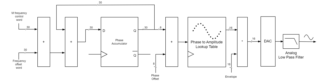
The above diagram shows a conceptual diagram of a DDFS system that supports all three modulation schemes.
Instead of sin(2* PI * f * t) the extended system generates:
A(t) * sin(2*PI*(f + Δf(t) * t ) + Δp(t))
- Frequency Control Word: Frequency control word (fccw) to generate the carrier frequency
- Frequency Offset Word: The frequency control word (focw) to generate the offset frequency Δf(t)
- Phase Offset: The phase value corresponding to the desired phase offset, Δp(t)
- Envelope: The digitized value of A(t)
DDFS module construction
The MiniZed Synth uses the following parameters in the design:
- fsys: 100 MHz
- N: 30 bits
- Width of the lookup table 8 bits (256 entries)
- sine wave amplitude resolution: 16 bits in signed format
The DDFS module can produce five different types of waveforms: Sinusoidal, Triangle, Square, Saw-Tooth, Noise, and any other wave based on the Phase to Amplitude Lookup Table as waveforms captured by a microphone.
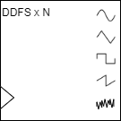
5.4. Sine Wave Generator
A sine wave, sinusoidal wave, or just sinusoid is a mathematical curve defined in terms of the sine trigonometric function, of which it is the graph. It is a type of continuous wave and also a smooth periodic function. By adding different sine waves we get a different waveform, which changes the timbre of the sound. When the sound is made up of more than one sinusoidal then it has more harmonics that are perceptible to the human ear.
The presence of higher harmonics in addition to the fundamental causes variation in the timbre, which is the reason why the same musical note (the same frequency) played on different instruments sounds different. The actual design can use the 3 oscillators with different variations in frequency and mix them.
Here the three main oscillators generate three different sinusoidal signals and an attenuated noise source. The fourth signal is the mixed signal.
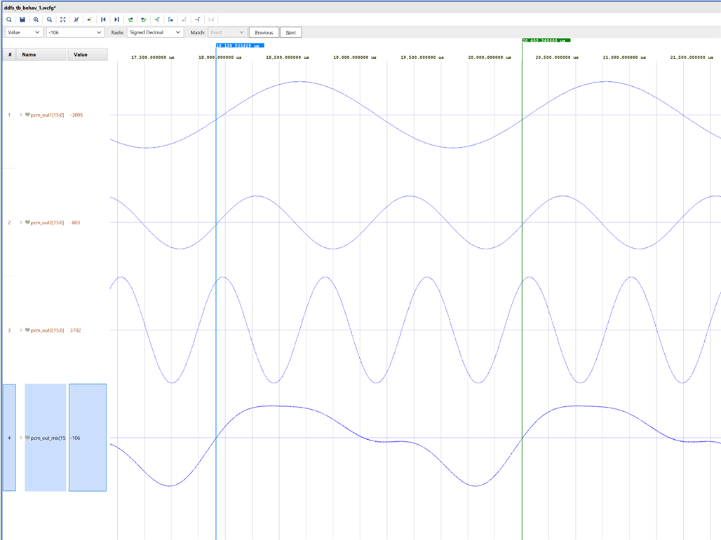
To generate the sinusoidal wave we can use algorithms like CORDIC or use a stored table with determined values and interpolation for intermediate values. For this project, the latter solution has been chosen.
Synchronous ROM Unit - Table Lookup
The size of the lookup table is 2^8 by 16 (4K bits)and can be implemented by a synchronous ROM.
The actual design will take advantage of the possibility to define the initial values of FPGA's internal memory modules. When an SRAM-based FPGA device is programmed, the configuration file is loaded into the device's configuration module. When the configuration is completed the memory modules are initialized as well. If the content of a memory is not updated during the operation, it maintains its original values and behaves like a ROM. This is an efficient way to implement large lookup tables or to store read-only data.
The read operation of a BRAM is controlled and synchronized by a clock signal. The ROM must include a clock signal as in the diagram.
After an address change, it takes one clock cycle to output new data. The ROM readout is buffered via a register.
The synchronous ROM is constructed with FPGA's BRAM module and its content is loaded into the BRAM's initial values when the device is configured.
The module uses an initial block to load the values using $readmemb directive.
Sine lookup table SystemVerilog Implementation
`timescale 1ns / 10ps

module sin_rom
#( parameter DATA_WIDTH = 16,  // number of bits
             ADDR_WIDTH = 8    // number od address bits

)
(
    input logic clk,
    input logic [ADDR_WIDTH-1:0] addr_r,
    output logic [DATA_WIDTH-1:0] dout
    );

    // signal declaration
    logic [DATA_WIDTH-1:0] ram [0:2**ADDR_WIDTH-1];  // ascending range
    logic [DATA_WIDTH-1:0] data_reg;

    initial
        $readmemh("sin_table.mem", ram);

    // read operation
    always_ff @(posedge clk)
    begin
        data_reg <= ram[addr_r];
    end

    assign dout = data_reg;
endmodule
DDFS module implementation in SystemVerilog
The DDFS module is built with two outputs pulse out that is a square wave and the Pulse Code Modulation (PCM) output with the selected waveform. The lookup table output (amp) and envelope are 16 bits wide. After multiplication, it needs to trim the 32-bit multiplication result back to 16 bits.
It uses Q2.14 format in which -1.0 and 1.0 are represented as 1100 0000 000 0000 and 0100 0000 0000 0000 respectively.
The multiplication result, modulation,
assign modulation = $signed(envelope) * $signed(amp);
is in the Q18.14 format. Finally, selects the appropriate portion of the modulation signal and trims it back to the Q16.0 format, a 16-bit signed integer.
`timescale 1ns / 1ps


module ddfs
#(parameter PHASE_ACC_WIDTH = 30) // width of phase accumulator
(
    input   logic               clk,
    input   logic               reset,
    input   logic   [PHASE_ACC_WIDTH-1:0]    freq_carrier_ctrl_word,     // frequency control word to generate carrier frequency
                                                                         // fccw = fout/fsys * 2^N ; (N = PHASE_ACC_WIDTH)
    input   logic   [PHASE_ACC_WIDTH-1:0]    freq_offset_ctrl_word,      // frequency offset control word
                                                                         // focw = fout/fsys * 2^N  ; (N = PHASE_ACC_WIDTH)
    input   logic   [PHASE_ACC_WIDTH-1:0]    phase_offset,               // phase offset
                                                                         // offset/360 * 2^N ; (N = PHASE_ACC_WIDTH)
    input   logic   [15:0]      envelope,                                // Amplitude modulation: envelope, digitized value of A(t) in Q2.14 format
    input   logic   [2:0]       wave_type,

    output  logic   [15:0]      pcm_out,                                 // pcm signal
    output  logic               pulse_out                                // pulse out
    );

    localparam SINE =     3'b000;
    localparam SQUARE =   3'b001;
    localparam SAW =      3'b010;
    localparam TRIANGLE = 3'b011;
    localparam NOISE =    3'b100;

    // signal declaration
    logic   [PHASE_ACC_WIDTH-1:0]    freq_control_word;  // frequency modulation control word
    logic   [PHASE_ACC_WIDTH-1:0]    phase_next;         // next phase
    logic   [PHASE_ACC_WIDTH-1:0]    phase_control_word; // phase control word
    logic   [PHASE_ACC_WIDTH-1:0]    phase_reg;          // actual phase
    logic   [7:0]       p2a_raddr;
    logic   [15:0]      amp;
    logic   signed  [31:0] modulation;
    logic   [15:0] pcm_reg;  // multi-bit PCM (pulse code modulation) t
    logic   [15:0] pcm_next;  // multi-bit PCM (pulse code modulation) t


    logic   [15:0] sine_amp;
    logic   [15:0] square_amp;
    logic   [15:0] triangle_amp;
    logic   [15:0] saw_tooth_amp;
    logic   [15:0] noise_amp;

    // body
    // instanciate sin() ROM
    sin_rom rom_unit
        (   .clk(clk),
            .addr_r(p2a_raddr),
            .dout(sine_amp));


   // instantiate square_wave unit
    square_wave square_unit
    (   .clk(clk),
        .addr_r(p2a_raddr),
        .dout(square_amp));

    // instantiate triangle wave unit
    triangle_wave triangle_unit
    (   .clk(clk),
        .addr_r(p2a_raddr),
        .dout(triangle_amp));

    // instantiate saw tooth wave unit
    saw_tooth saw_tooth_unit
    (   .clk(clk),
        .addr_r(p2a_raddr),
        .dout(saw_tooth_amp));

    // instantiate lsfr noise
    lfsr lfsr_unit(.clk(clk),
             .enable(1'b1),
             .lfsr_data(noise_amp),
             .reset(reset));

    // phase register and output buffer
    // use an output buffer (to shorten crtical path since the o/p feeds dac)
    // always_ff @(posedge clk)
    //    pcm_reg <= modu[29:14];
    always_ff @(posedge clk, posedge reset)
    begin
        if (reset)
            begin
                phase_reg <= 0;
                pcm_reg <= 0;
            end
        else
            begin
                phase_reg <= phase_next;
                pcm_reg <= pcm_next;
            end
    end

    // frequency modulation
    assign freq_control_word = freq_carrier_ctrl_word + freq_offset_ctrl_word;

    // phase accumulation
    assign phase_next = phase_reg + freq_control_word;

    assign pcm_next = modulation[29:14];

    // phase modulation
    assign phase_control_word = phase_reg + phase_offset;

    // phase to amplitude mapping address
    assign p2a_raddr = phase_control_word[PHASE_ACC_WIDTH-1:PHASE_ACC_WIDTH-8]; // 8 bits

    // amplitude modulation envelop in Q2.14
    //    * -1 < env < +1  (between 1100...00 and 0100...00)
    //    * Q16.0 * Q2.14 => modu is Q18.14
    //    * convert modu back to Q16.0
    // assign modulation = $signed(envelope) * $signed(amp);

    always_comb begin
      case (wave_type)
          SINE    : amp = sine_amp;
          SQUARE  : amp = square_amp;
          SAW     : amp = saw_tooth_amp;
          TRIANGLE: amp = triangle_amp;
          NOISE   : amp = noise_amp;
          default:  amp = sine_amp;
       endcase
       modulation = $signed(envelope) * $signed(amp);
    end

    assign pcm_out = pcm_reg;
    assign pulse_out = phase_reg[PHASE_ACC_WIDTH-1];

endmodule
Test Bench
- T = 4,545.96µs - 2,273.01µs = 2,273 μs (microseconds)
- Frequency ν from ν = 1/T = 439.956884 Hz ≈ 440 Hz (hertz)
- Jitter 440 - 439.956884 = 0.043116 s
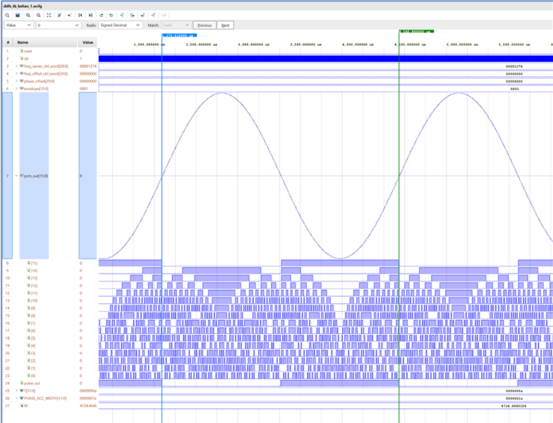
5.5. Noise Generator Module
Noise is characterized as being aperiodic or having a non-repetitive pattern. White noise is a type of sound that contains all audible frequencies in equal amounts. It sounds like a hiss or a static noise. In sound synthesizers, white noise is used as a starting point for creating other sounds. By adding filters or modulating the sound, the synthesizer can create different tones or textures.
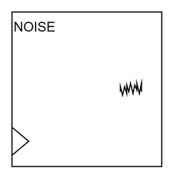
A few examples of sounds that can be created using white noise as a starting point are the sound of a snare drum and the sound of the wind. the sound of ocean waves, the sound of cymbals...
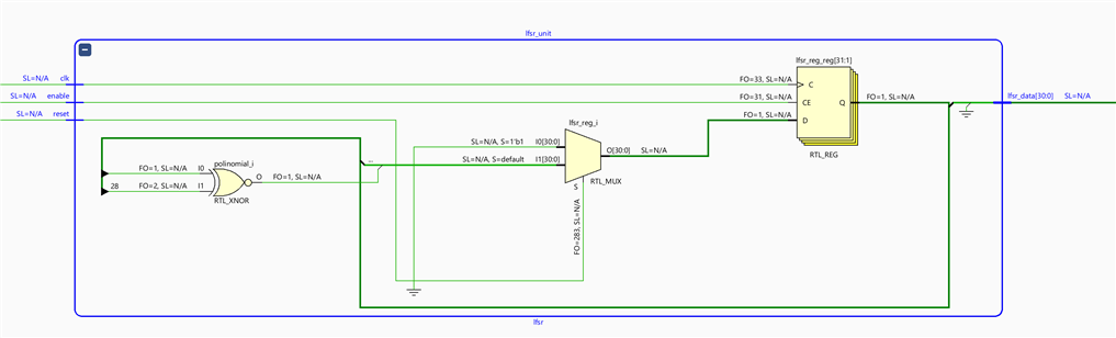
For noise generation, this module uses a linear-feedback shift register (LFSR). An LFSR is a shift register whose input bit is a linear function of its previous state. The most commonly used linear function of single bits is exclusive-or (XOR). Thus, an LFSR is most often a shift register whose input bit is driven by the XOR of some bits of the overall shift register value. Any long LFSR counter generates a long pseudo-random sequence of zeros and ones. The sequence is not exactly random since it repeats eventually, and it also follows a mathematically predictable sequence.
Vivado synthesis for the SystemVerilog module
The appropriate taps for Maximum-Length LFSR Counters are extracted from this Xilinx Technical Note:
xapp052.pdf • Viewer • AMD Adaptive Computing Documentation Portal (xilinx.com)
SystemVerilog implementation of the Noise module using a Linear Feedback Shift Register
`timescale 1ns / 1ps

// Description:
//  This module generates an 16-bit random number. A LFSR or Linear Feedback Shift Register
//  is a quick and easy way to generate pseudo-random data inside of an FPGA.

module lfsr #(parameter NUM_BITS = 31)
  (
   input logic clk,
   input logic reset,
   input logic enable,
   output logic [NUM_BITS-1:0] lfsr_data
   );

  logic [NUM_BITS:1] lfsr_reg = 0;
  logic polinomial;

  // run LFSR when enabled.
  always @(posedge clk, posedge reset)
    begin
      if (enable == 1'b1)
        begin
            if (reset == 1'b1) begin
                lfsr_reg <= 1'b0;
            end else begin
                lfsr_reg <= {lfsr_reg[NUM_BITS-1:1], polinomial};
            end
        end else begin
            lfsr_reg <= lfsr_reg;
        end
    end

  // Feedback Polynomial based on Xilinx Application Note:
  // http://www.xilinx.com/support/documentation/application_notes/xapp052.pdf
  // for 16 bits
  // assign  polinomial = lfsr_reg[16] ^~ lfsr_reg[15] ^~ lfsr_reg[13] ^~ lfsr_reg[4];
  // for 31 bits
   assign  polinomial = lfsr_reg[31] ^~ lfsr_reg[28];

  assign lfsr_data = lfsr_reg[16:1];

endmodule
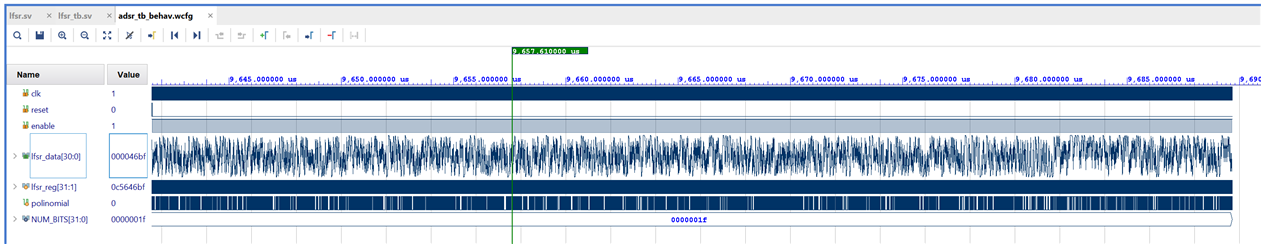
5.6. Square Wave Generator
A square wave is a non-sinusoidal periodic waveform in which the amplitude alternates at a steady frequency between fixed minimum and maximum values, with the same duration at minimum and maximum. In an ideal square wave, the transitions between minimum and maximum are instantaneous, Square waves contain a wide range of harmonics. The ideal square wave contains only components of odd-integer harmonic frequencies.
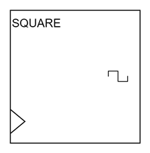
In music, they are described as hollow sounds. They can be used as the basis for wind instrument sounds created using subtractive synthesis.
Also for performing distortion effects by clipping the outermost regions of the waveform, making it more and more like a square wave as more distortion is applied.
SystemVerilog implementation for the square wave generator.
`timescale 1ns / 1ps

/**
A square wave is a non-sinusoidal periodic waveform
in which the amplitude alternates at a steady frequency between
fixed minimum and maximum values, with the same duration at minimum and maximum.
n musical terms, they are often described as sounding hollow, and are therefore
used as the basis for wind instrument sounds created using subtractive synthesis.
Additionally, the distortion effect used on electric guitars clips the outermost
regions of the waveform, causing it to increasingly resemble
a square wave as more distortion is applied.
*/
module square_wave
#( parameter DATA_WIDTH = 16,  // number of bits
             ADDR_WIDTH = 8    // number od address bits

)
(
    input logic clk,
    input logic [ADDR_WIDTH-1:0] addr_r,
    output logic [DATA_WIDTH-1:0] dout
    );

    // signal declaration
    logic [DATA_WIDTH-1:0] data_reg;
    logic [DATA_WIDTH-1:0] data;


    // read operation
    always_ff @(posedge clk)
    begin
        data_reg <= data;
    end

    always_comb
    begin
       data = addr_r[7]?16'b1100_0000_0000_0000:16'b0100_0000_0000_0000;
    end

    assign dout = data_reg;
endmodule
5.7. Triangle Wave Generator
A triangular wave or triangle wave is a non-sinusoidal waveform named for its triangular shape. It is a periodic, piecewise linear, continuous real function. Like a square wave, the triangle wave contains only odd harmonics. However, the higher harmonics roll off much faster than in a square wave (proportional to the inverse square of the harmonic number as opposed to just the inverse).
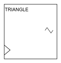
Triangle Wave Generator - SystemVerilog implementation
`timescale 1ns / 10ps

/**
A triangular wave or triangle wave is a non-sinusoidal waveform
named for its triangular shape. It is a periodic, piecewise linear,
continuous real function. Like a square wave, the triangle wave
contains only odd harmonics.
The higher harmonics roll off much faster than in a square wave.
*/

module triangle
#( parameter DATA_WIDTH = 16,  // number of bits
             ADDR_WIDTH = 8    // number od address bits

)
(
    input logic clk,
    input logic [ADDR_WIDTH-1:0] addr_r,
    output logic [DATA_WIDTH-1:0] dout
    );

    // signal declaration
    logic [DATA_WIDTH-1:0] data_reg;
    logic [DATA_WIDTH-1:0] data;

    // read operation
    always_ff @(posedge clk)
    begin
        data_reg <= data;
    end

    always_comb
    begin
      if (addr_r > 8'h7F) begin
           data = {8'h00, 8'hFE - addr_r}; // decaying
      end else begin
           data = {8'h00, addr_r}; // raising
      end
    end

    assign dout =  $signed(data << 9) - $signed(16'h8000);  // offset biass
endmodule
5.8. Saw-Tooth Wave Generator Module
Sawtooth waves and real-world signals contain all integer harmonics.
`timescale 1ns / 10ps


module saw_tooth
#( parameter DATA_WIDTH = 16,  // number of bits
             ADDR_WIDTH = 8    // number od address bits

)
(
    input logic clk,
    input logic [ADDR_WIDTH-1:0] addr_r,
    output logic [DATA_WIDTH-1:0] dout
    );

    // signal declaration
    logic [DATA_WIDTH-1:0] data_reg;
    logic [DATA_WIDTH-1:0] data;
    logic [DATA_WIDTH-1:0] amp;


    // read operation
    always_ff @(posedge clk)
    begin
        data_reg <= data;
    end


    always_comb
    begin
      amp = {8'h00, addr_r} << 8;
      data = $signed(amp) - $signed(16'h8000);
    end


    assign dout = data_reg;
endmodule
5.9. Attack-Decay-Sustain-Release (ADSR) Envelope Modulation
The ATTACK-DECAY-SUSTAIN-RELEASE (ADSR) envelope modulation scheme is based on the observation that when a real instrument generates a note, the volume of the musical note changes over time. It rises rapidly from zero and then steadily decays. To model this effect we can multiply the constant tone produced by the DDFS module by an amplitude ADSR envelope that contains the segments, attack, decay, sustain, and release. As can be seen in the figure below:

The ADRS envelope can be specified by two amplitude parameters, A max and Asus, and four time parameters, Attack time, Decay time, Sustain time, and Release time.
- A max: maximum amplitude level the envelope can reach.
- A sus: the amplitude of the sustain segment.
- Attack time: the time interval of the Attack segment.
- Decay time: the time interval of the Decay segment.
- Sustain time: the time interval of the Sustain segment.
- Release time: the time interval of the Release segment.
The maximum level will be defined as a constant and the sustain level will be defined as a percentage of the maximum amplitude. So we only need 6 parameters to define an envelope.
ADSR Envelope Generator Circuit
The ADSR Envelope Generator is a circuit that generates an amplitude envelope following the ADSR scheme.
The ADSR circuit models the sound generation of a musical instrument and its output does not run continuously.
A single envelope is generated at a time and the generation is controlled by a start trigger signal.
The trigger signal can be triggered automatically or in real-time mode:
- The automatic mode uses the trigger signal as a note start.
- The real-time mode mimics the operation of a key on the piano keyboard.
In the real-time mode, when the trigger signal is asserted, the envelope circuit will start operation and remain in the sustain segment until the trigger signal is canceled.
Finite State Machine with Data Path (FSMD) design of the ADSR Envelope Generator
The ADSR envelope generator is created using an FSMD with an amplitude counter and a sustained time counter. An FSMD is a kind of finite-state machine with a Data Path.
A Finite-State Machine (FSM) is a sequential circuit that can be in exactly one of a finite number of states at any given time.
It contains five elements:
- symbolic state register
- input signal
- output signal
- current state
- next state computed by a function
The symbolic state register contains the state. The FSM has a function to computer the next state and depending on the current state has an output (Moore FSM), and maybe on the input and the current state (Mealy FSM).
A traditional FSM cannot represent storage elements (register) except the state registers. We can use instead an FSMD. An FSM with a Datapath (FSMD) is an extension of a traditional FSM. The storage and signals can be declared. and within a state expression, comparison, arithmetic, or logic operations on these signals can be performed.
The behavior of the ADSR envelope is represented by this FSMD circuit with an Algorithmic State Machine Chart or ASM chart, a flow-chart-like description constructed from ASM blocks: state boxes, decision boxes, and conditional output boxes.
This is the graphical representation of a generic ASM block for a state.

The unconditional outputs corresponding to that state can be placed inside the state box. Moore state machine outputs can also be placed inside the state box.
In general, Mealy state machine outputs are represented inside a conditional output box.
In addition to the attack, decay, sustain, and release states we'll add an idle state for the idle condition and a launch state for the retriggering.
The start signal is the trigger to initiate the amplitude envelope generation.
Once asserted the FSMD goes through the entire envelope generation process unless the start signal is asserted before completion, in that case, the FSMD aborts the current operation and starts a new envelope generation. The start signal is checked in every state.
The FSMD uses two registers, amplitude and t_sus, for the amplitude counter and the sustain counter.

The FSM uses the attack, decay, sustain, and release states to represent the four segments of the ADS envelope.
The amplitude counter is used to generate the envelope amplitude. It is also used to determine the time spent in the attack, decay, and release states. In each state, the amplitude is decremented or incremented by a specific amount every clock cycle.
The value used for increment or decrement of the counter in those states is passed pre-calculated to the ADSR envelope generator module: attack step, decay_step, and release_step.
The ADRS envelope can be specified by:
- Attack_ms: The time interval (t_attack ) between activation and full loudness (MAX).
- Decay_ms: The time interval (t_decay) for Vmax to drop to the sustain level (Sustain_level).
- Sustain_level: The constant sound volume (Sustain_level) for the note until it is released.
- Release_ms: The time interval (t_release ) for the sound to fade from Vs to 0 when a note ends.
Attack_step: amount the amplitude counter must be incremented each clock cycle to reach MAX from zero in t_attack time
Attack_step = (MAX- 0)/(t_attack / t_sys)
- MAX: the maximum amplitude as MAX, the sustained amplitude as sustain_level
- t_attack: time in the attack segment
- t_sys: system time, depends on system clock frequency
Decay_step: amount the amplitude counter must be decremented each clock cycle to reach the sustain level amplitude from MAX in t_decay time
Decay_step = (MAX-sustain_level) / (t_decay / t_sys)
- sustain_level: amplitude in the sustain segment
- t_decay: time in the decay segment
- t_sys: system time, depends on system clock frequency
Release_step: amount the amplitude counter must be decremented each clock cycle to reach the zero level amplitude from the sustain_level in t_release time
Release_step = (Sustain_level-0) / (t_release / t_sys)
- sustain_level: amplitude in the sustain segment
- t_release: time in the release segment
- t_sys: system time, depends on system clock frequency
Sustain_time: the number of clock cycles in the sustain segment. The amplitude is constant in the sustain segment and its interval is controlled by the sustain time.
sustain_time = t_sustain / t_sys
- t_sustain: time in the sustain segment
- t_sys: system time, depends on system clock frequency
The incrementing and decrementing steps appear as external circuit signals, Attack_step, Decay_step, Decay_step. The Sustain_level also appears as an external circuit signal.
- After the start is asserted, the FSMD moves from the idle state to the launch state.
- Then the FSM moves to the attack state, where the amplitude register is incremented with the Attack_step until it reaches the MAX amplitude.
- Then the FSMD transits to the decay state in which the amplitude register is decremented with the Decay_step until the amplitude reaches the Sustain_level.
- Then the FSMD transits to the sustain state in which the t_sus register is incremented until reaching Sustain_time.
- Then the FSMD moves to the release state in which the amplitude register is decremented until it becomes 0.
- Then the FSMD returns to the idle state.
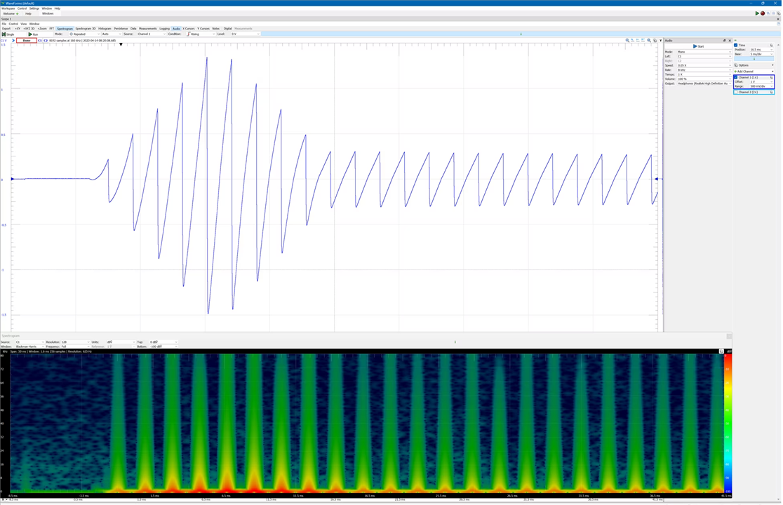
ADSR envelope applied to a Saw-Tooth Wave
ADSR Envelope Generator SystemVerilog implementation
`timescale 1ns / 1ps


// fsm to generate ADSR envelop

// start (trigger) signal:
//     - starts the "attack" when asserted
//     - restarts the epoch if aseerted before the current epoch ends

// amplitudes:
//     - 32-bit unsigned
//     - use 32 bits to accommodate the needed resolution for "step"
//     - intepreted as Q1.31 format:
//     - range artificially limited between 0.0 and 1.0
//     - i.e., 0.0...0 to 1.0...0 (1.0)
//     - 1.1xx...x not allowed

// output: Q2.14 for range (-1.0 to 1.0)

// special atk_step values
//     - atk_step = 11..11: bypass adsr; i.e., envelop=1.0
//     - atk_step = 00..00: output 0; i.e., envelop = 0.0

// Width selection:
//   max attack time = 2^31 * clock period = 2^31 *(1/100e6) = 21,47483648 seconds

// Attack_time
// t_attack desired attack time
// t_sys sytem clock period
// maximum amplitude Amax
// need t_attack / t_sys clock cycles in the attact segment
// the counter must be incremented (Amax - 0)/(t_attack - t_sys) each clock cycle to reach A_max from zero in t_attack

// Decrementing amount in decay segment for t_decay
// t_decay and A_sus.  (A_max-A_sus) / (t_sustain / t_sys)
//

// Decrementing amount in release segment
// (A_sus - 0)/(t_release - t_sys)

// The amplitude is constant in the sustain segment
// There are are tsustain / t_sys cycles in the sustain segment

// Amax  |    /\
//       |   /  \
//       |  /    \
// Asus  | /      ------------
//       |/                   \
//       ---------------------------
//        | attack
//             | decay
//                | sustain
//                            | release


 module adsr(
input logic clk,
input logic reset,
input logic start, // generate a pulse to start the envelope generation
input logic [31:0] attack_step_value, // precalculated (Amax - 0)/(t_attack - t_sys) steps for the attack segment
input logic [31:0] decay_step_value,  // precalculated (A_max-A_sus) / (t_sustain / t_sys) steps for the decay segment
input logic [31:0] sustain_level, // amplitude for the sustain segment
input logic [31:0] release_step_value,  // precalculated (A_sus - 0)/(t_release - t_sys) steps fot the release segment
input logic [31:0] sustain_time, // tsustain / t_sys steps for the sustain
output logic [15:0] envelope,
output logic adsr_idle

    );

    // constants
    localparam MAX = 32'h8000_0000;
    localparam BYPASS = 32'hffff_ffff;
    localparam ZERO = 32'h0000_0000;

    // fsm state type
    typedef enum {idle, launch, attack, decay, sustain, rel} state_type;

    // declaration
    state_type state_reg;
    state_type state_next;
    logic [31:0] amplitude_counter_reg;
    logic [31:0] amplitude_counter_next;
    logic [31:0] sustain_time_reg;
    logic [31:0] sustain_time_next;
    logic [31:0] n_tmp;
    logic fsm_idle;
    logic [31:0] envelope_i;

    // state and data registers
    always_ff @(posedge clk, posedge reset)
    begin
        if(reset)
          begin
            state_reg <= idle;
            amplitude_counter_reg <= 32'h0;
            sustain_time_reg <= 32'h0;
          end
         else
         begin
            state_reg <= state_next;
            amplitude_counter_reg <= amplitude_counter_next;
            sustain_time_reg <= sustain_time_next;
         end
    end

    // fsmd next-state logic and data path logic
    always_comb
    begin
        state_next = state_reg;
        amplitude_counter_next = amplitude_counter_reg;
        sustain_time_next = sustain_time_reg;
        fsm_idle = 1'b0;
        case (state_reg)
            idle: begin
                fsm_idle = 1'b1;
                if (start) begin
                    state_next = launch;
                  end
              end
            launch: begin
                state_next = attack;
                amplitude_counter_next = 32'b0;
              end
            attack: begin
                if(start) begin
                    state_next = launch;
                end else begin
                    n_tmp = amplitude_counter_reg + attack_step_value;
                    if (n_tmp < MAX) begin
                        amplitude_counter_next = n_tmp;
                    end else begin
                        state_next = decay;
                    end
                 end
              end
            decay: begin
                if (start) begin
                    state_next = launch;
                end else begin
                    n_tmp = amplitude_counter_reg - decay_step_value;
                    if(n_tmp > sustain_level) begin
                        amplitude_counter_next = n_tmp;
                    end else begin
                        amplitude_counter_next = sustain_level;
                        state_next = sustain;
                        sustain_time_next = 32'b0;  // start timer
                    end
                 end
              end
            sustain: begin
                if (start) begin
                    state_next = launch;
                end else begin
                    if(sustain_time_reg < sustain_time) begin
                        sustain_time_next = sustain_time_next + 1;
                    end else begin
                        state_next = rel;
                    end
                 end
              end
             default: begin
                if (start) begin
                    state_next = launch;
                  end else begin
                    if(amplitude_counter_reg > release_step_value) begin
                        amplitude_counter_next = amplitude_counter_reg - release_step_value;
                    end else begin
                        state_next = idle;
                    end
                  end
               end
        endcase

    end

    assign adsr_idle = fsm_idle;

    assign envelope_i = (attack_step_value == BYPASS) ? MAX :
                   (attack_step_value == ZERO) ? 32'b0 :
                   amplitude_counter_reg;

    assign envelope = {1'b0, envelope_i[31:17]};
endmodule
Direct capture of the MiniZed Synth. Two triangular waves added out of phase, with frequency modulation using an LFO, and sculpted with the ADSR envelope of the final amplifier.
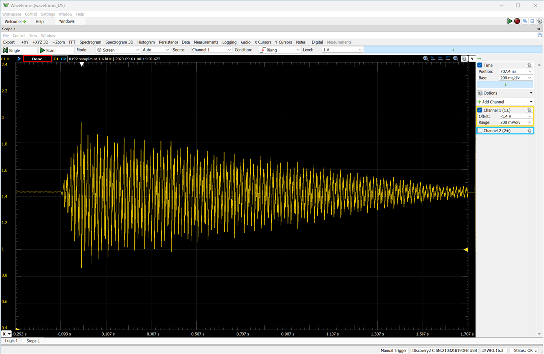
Direct capture of the MiniZed Synth with the Digilent Analog Discovery 2.
In the real-time mode, when the trigger signal is asserted, the envelope circuit will start operation and remain in the sustain segment until the trigger signal is canceled.
Here is an implementation in SystemVerilog. Please note that the hold time is no longer indicated.
`timescale 1ns / 1ps
// adsr with real time option
// sus_time is controlled by the sart signal instead of sustain_time

// fsm to generate ADSR envelop

// start (trigger) signal:
//     - starts the "attack" when asserted
//     - restarts the epoch if aseerted before the current epoch ends

// amplitudes:
//     - 32-bit unsigned
//     - use 32 bits to accommodate the needed resolution for "step"
//     - intepreted as Q1.31 format:
//     - range artificially limited between 0.0 and 1.0
//     - i.e., 0.0...0 to 1.0...0 (1.0)
//     - 1.1xx...x not allowed

// output: Q2.14 for range (-1.0 to 1.0)

// special atk_step values
//     - atk_step = 11..11: bypass adsr; i.e., envelop=1.0
//     - atk_step = 00..00: output 0; i.e., envelop = 0.0

// Width selection:
//   max attack time = 2^31 * clock period = 2^31 *(1/100e6) = 21,47483648 seconds

// Attack_time
// t_attack desired attack time
// t_sys sytem clock period
// maximum amplitude Amax
// need t_attack / t_sys clock cycles in the attact segment
// the counter must be incremented (Amax - 0)/(t_attack - t_sys) each clock cycle to reach A_max from zero in t_attack

// Decrementing amount in decay segment for t_decay
// t_decay and A_sus.  (A_max-A_sus) / (t_sustain / t_sys)
//

// Decrementing amount in release segment
// (A_sus - 0)/(t_release - t_sys)

// The amplitude is constant in the sustain segment
// Keeps in the sustain segment while start is asserted

// Amax  |    /\
//       |   /  \
//       |  /    \
// Asus  | /      ------------
//       |/                   \
//       ---------------------------
//        | attack
//             | decay
//                | sustain
//                            | release


 module adsr_rt(
input logic clk,
input logic reset,
input logic start, // start the envelop and sustain signal
input logic [31:0] attack_step_value, // precalculated (Amax - 0)/(t_attack - t_sys) steps for the attack segment
input logic [31:0] decay_step_value,  // precalculated (A_max-A_sus) / (t_sustain / t_sys) steps for the decay segment
input logic [31:0] sustain_level, // amplitude for the sustain segment
input logic [31:0] release_step_value,  // precalculated (A_sus - 0)/(t_release - t_sys) steps fot the release segment
output logic [15:0] envelope,
output logic adsr_idle

    );

    // constants
    localparam MAX = 32'h8000_0000;
    localparam BYPASS = 32'hffff_ffff;
    localparam ZERO = 32'h0000_0000;

    // fsm state type
    typedef enum {idle, launch, attack, decay, sustain, rel} state_type;

    // declaration
    state_type state_reg;
    state_type state_next;
    logic [31:0] amplitude_counter_reg;
    logic [31:0] amplitude_counter_next;
    logic [31:0] n_tmp;
    logic fsm_idle;
    logic [31:0] envelope_i;

    // state and data registers
    always_ff @(posedge clk, posedge reset)
    begin
        if(reset)
          begin
            state_reg <= idle;
            amplitude_counter_reg <= 32'h0;
          end
         else
         begin
            state_reg <= state_next;
            amplitude_counter_reg <= amplitude_counter_next;
         end
    end

    // fsmd next-state logic and data path logic
    always_comb
    begin
        state_next = state_reg;
        amplitude_counter_next = amplitude_counter_reg;
        fsm_idle = 1'b0;
        case (state_reg)
            idle: begin
                fsm_idle = 1'b1;
                if (start) begin
                    state_next = launch;
                  end
              end
            launch: begin
                state_next = attack;
                amplitude_counter_next = 32'b0;
              end
            attack: begin
                if(!start) begin
                    state_next = rel;
                end else
                 begin
                    n_tmp = amplitude_counter_reg + attack_step_value;
                    if (n_tmp < MAX) begin
                        amplitude_counter_next = n_tmp;
                    end else begin
                        state_next = decay;
                    end
                 end
              end
            decay: begin
                if (!start) begin
                    state_next = rel;
                end else
                begin
                    n_tmp = amplitude_counter_reg - decay_step_value;
                    if(n_tmp > sustain_level) begin
                        amplitude_counter_next = n_tmp;
                    end else begin
                        amplitude_counter_next = sustain_level;
                        state_next = sustain;
                    end
                 end
              end
            sustain: begin
                if (!start) begin
                    state_next = rel;
                end else begin
                    state_next = sustain;
                 end
              end
             default: begin
                if (start) begin
                    state_next = launch;
                  end else begin
                    if(amplitude_counter_reg > release_step_value) begin
                        amplitude_counter_next = amplitude_counter_reg - release_step_value;
                    end else begin
                        state_next = idle;
                    end
                  end
               end
        endcase

    end

    assign adsr_idle = fsm_idle;

    assign envelope_i = (attack_step_value == BYPASS) ? MAX :
                   (attack_step_value == ZERO) ? 32'b0 :
                   amplitude_counter_reg;

    assign envelope = {1'b0, envelope_i[31:17]};
endmodule
A test bench checking correct operation.
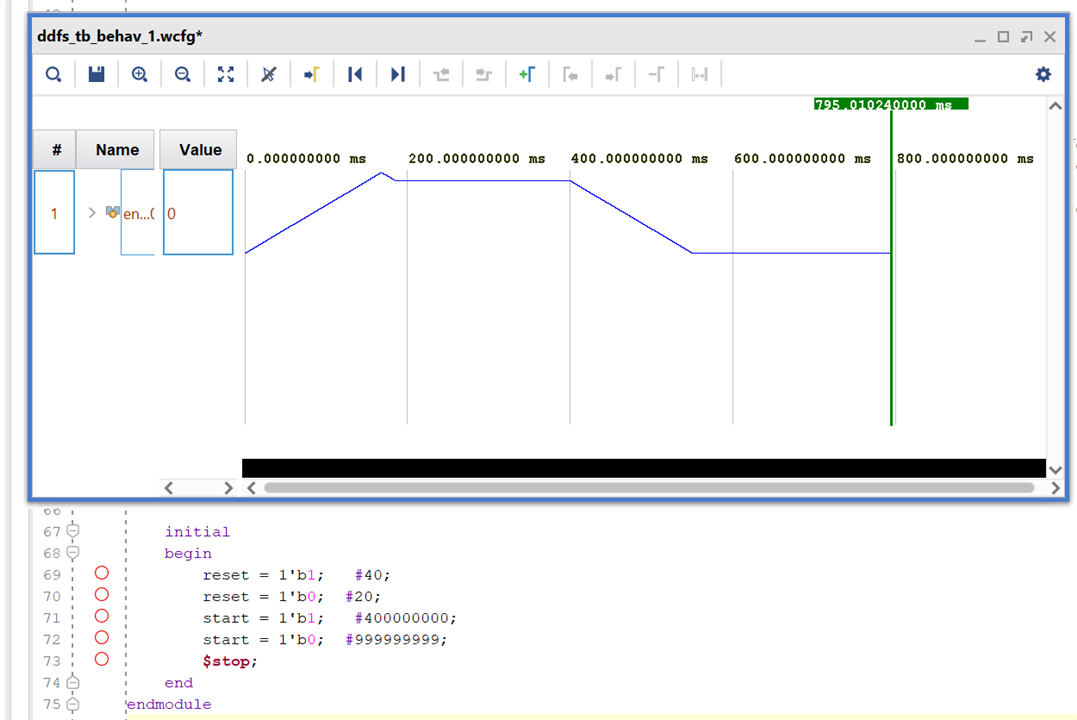
5.10. One-bit delta-sigma DAC
To convert the PCM signal to a true analog signal it is needed a DAC (digital-to-analog converter) and a low-pass filter.
The system uses a one-bit-delta-sigma DAC, which generates PDM (pulse modulation) output. This DAC can be realized in pure digital logic without any analog component. See Analog-Sigma-Delta ADCs and DACs
The frequency of the system clock is 100MHz and the frequency of the generated audio signal is around 20kHz.
Delta-Sigma DACs are high-speed single-bit DACs. Using digital feedback, a string of pulses is generated. The average duty cycle of the pulse string is proportional to the value of the binary input. The analog signal is created by passing the pulse string through an analog low-pass filter.
Conceptual Design
Conceptual block diagram of a one-bit delta-sigma DAC.
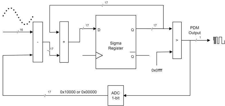
It consists of a one-bit delta-sigma modulation circuit and a one-bit ADC. The term, Delta-Sigma, refers to the arithmetic difference and sum, respectively.
The PCM input is in the 16-bit unsigned integer format. from 0x0000 to 0xffff. Data is expanded to 17 bits internally.
The Sigma Accumulator is the main part of the DAC, composed of an adder and a register. It continuously adds the input PCM data samples.
If the accumulation exceeds the maximum value of 0xffff, the PDM pulse becomes '1' and the amount of 0x1_0000 is subtracted from the accumulation.
The one-bit ADC converts logic '0' and '1' into two PC values of 0x0_0000 and 0x1_0000.
More high pulses will be generated if the PCM amplitude is larger.
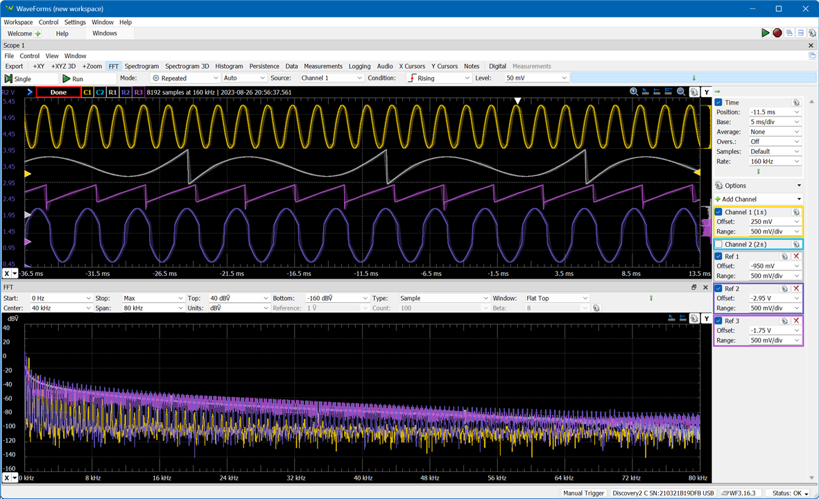
Different sound waves generated mixing different waves and converted to analog by the 1-bit delta sigma DAC after the RC low-pass filter
One-bit Delta Sigma SystemVerilog Implementation
The comparator can be eliminated, we can use the MSB as the output. The subtractor also can be eliminated. We can simply append a 0 to the 16 LSBs and use it as the feedback value. The output of the amplifier converted from a 16-bit signed format to a 17-bit unsigned format. It is first sign-extended to 17 bits and then added a bias of 0x0_ 8000
`timescale 1ns / 10ps

module ds_1bit_dac
#(parameter W = 16)  // input width
(
input logic clk,
input logic reset,
input logic [W-1:0] pcm_in,
output logic pdm_out
    );

    // signal declarations
    localparam BIAS = 2 ** (W-1); // {1'b1, (W-2){1'b0}};
    logic [W:0] pcm_biased;
    logic [W:0] acc_next;
    logic [W:0] acc_reg;

    // shift the range from [-2^(W-1) -1 , 2^(W-1)-1] to [0, 2^W-1]
    assign pcm_biased = {pcm_in[W - 1], pcm_in} + BIAS;

    // signal treated as unsigned number in delta-sigma modulation
    assign acc_next = {1'b0, acc_reg[W-1:0]} + pcm_biased;

    // accumulation register
    always_ff @(posedge clk, posedge reset)
    begin
        if (reset)
        begin
            acc_reg <= 0;
        end
        else
        begin
            acc_reg <= acc_next;
        end
    end

    assign pdm_out = acc_reg[W];


endmodule
5.11. Mixer Module
The mixer module is very simple. It takes the input audio signals, mixes them, and provides one output signal.
`timescale 1ns / 1ps
//////////////////////////////////////////////////////////////////////////////////
// Company:
// Engineer:
//
// Create Date: 08/19/2023 11:21:59 AM
// Design Name:
// Module Name: mixer
// Project Name:
// Target Devices:
// Tool Versions:
// Description:
//
// Dependencies:
//
// Revision:
// Revision 0.01 - File Created
// Additional Comments:
//
//////////////////////////////////////////////////////////////////////////////////


module mixer(
    input logic clk,
    input logic reset,
    input logic [15:0] input_1, // input signal 1
    input logic [15:0] lvl_1, // volume level 1
    input logic [15:0] input_2, // input signal 2
    input logic [15:0] lvl_2, // volume level 2
    input logic [15:0] input_3, // input signal 3
    input logic [15:0] lvl_3, // volume level 3
    input logic [15:0] input_4, // input signal 4
    input logic [15:0] lvl_4, // volume level 4
    output logic [15:0] pcm_out
    );

    logic   signed  [31:0] modulation1;
    logic   signed  [31:0] modulation2;
    logic   signed  [31:0] modulation3;
    logic   signed  [31:0] modulation4;
    logic   signed  [31:0] sum;

    // amplitude modulation in Q2.14
    //    * -1 < env < +1  (between 1100...00 and 0100...00)
    //    * Q16.0 * Q2.14 => modu is Q18.14
    //    * convert modu back to Q16.0
    // assign modulation = $signed(envelope) * $signed(amp);

    assign modulation1 = $signed(lvl_1) * $signed(input_1);
    assign modulation2 = $signed(lvl_2) * $signed(input_2);
    assign modulation3 = $signed(lvl_3) * $signed(input_3);
    assign modulation4 = $signed(lvl_4) * $signed(input_4);

    // Q18.14 + Q18.14 = Q18.14
    assign sum = $signed( modulation1 + modulation2 + modulation3 + modulation4);
    // TODO overflow treatment with clipping

    // convert back to Q16.0
    assign pcm_out = sum[29:14];

endmodule
In the next image, the mixer combines a triangle wave, a square wave, and a sinusoidal wave.

5.12. Filter Module
The filters have the function of altering the spectral content of the signal generated by the oscillators, increasing, attenuating, or even filtering certain harmonics. To do this, resonant filters are used, with a cut-off frequency and quality factor (Q, hereinafter, resonance) that can be parameterized by the user interactively. The filter should be a variable filter that allows adjustment of the cutoff frequency and resonance level, since depending on the frequency and type of signal generated by the oscillator, these parameters will be adjusted differently to obtain the desired timbre. The parameter setting can be done manually, by the user, or using modulations with ADSR envelopes, which provides a high degree of dynamism to the generated sound.
A low-pass filter based on a moving average has been developed.
`timescale 1ns / 1ps
///////////////////////////////////////////////////////////////////////


module moving_average_lpf(
    input logic clk,
    input logic reset,
    input logic [7:0] order,
    input logic  [15:0] signal_in,
    output logic  [15:0] signal_out
);


    // signal declarations
    localparam BIAS = 2 ** 15; // {1'b1, (W-2){1'b0}};

    logic [31:0] ma_new, ma_new_reg;
    logic [31:0] ma_old, ma_old_reg;
    logic [31:0] signal_n;
    logic [16:0] unbiased_signal_out;
    logic [16:0] biased_signal;
    logic [16:0] biased_trucated_output;


    // shift the range from [-2^(15) -1 , 2^(15)-1] to [0, 2^32-1]
    assign biased_signal = {signal_in[15], signal_in} + BIAS;

    assign signal_n = {biased_signal, 15'b0};

    always_ff @(posedge clk, posedge reset) begin
        if (reset) begin
            ma_new_reg <=0;
            ma_old_reg <=0;
        end else begin
            ma_new_reg <= ma_new;
            ma_old_reg <= ma_old;
        end
    end


    assign ma_old = ma_new_reg;
    assign ma_new = $signed(signal_n  >> order) + $signed(ma_old_reg) - $signed(ma_old_reg >> order) ;

    assign biased_trucated_output = ma_new_reg[31:15];


    assign unbiased_signal_out = $signed(biased_trucated_output - BIAS) ;

    assign signal_out = unbiased_signal_out[15:0];

endmodule
A noise signal after filtered and unfiltered with order = 6
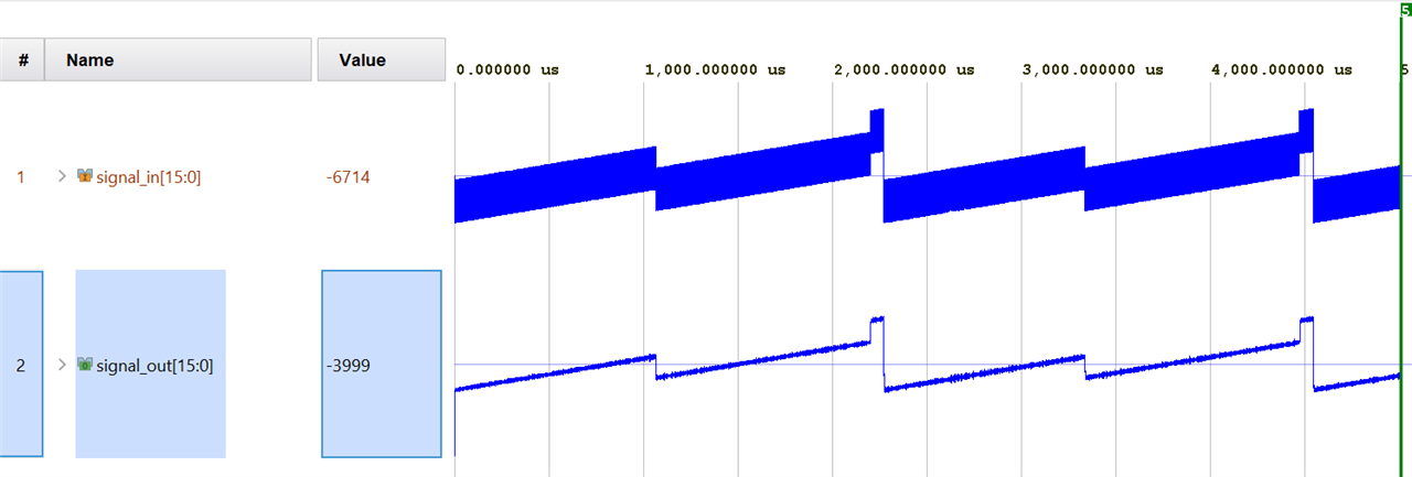
And with order = 12
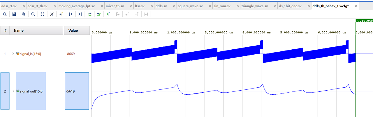
The final design will have a version of the Chamberlin state-variable filter. I haven't finished implementing yet.
The Chamberlin provides multiple outputs with different filtering characteristics.
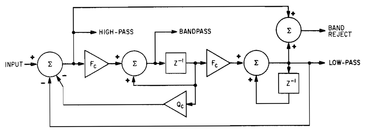
Controlling the feedback path, you can change the filter's resonance and emphasize specific frequency ranges.
5.13. Amplifier Module
The function of the amplifier module is to shape the amplitude in time, for this it multiplies the output of the ADSR module by the output of the mixer to then pass the signal to the final filter.
Again, fixed point encoding numbers are used to avoid floating point operations.
module amplifier(
    input logic clk,
    input logic reset,
    input logic [15:0] pcm_input,
    input logic [15:0] envelope, // Amplitude modulation: envelope, digitized value of A(t) in Q2.14 format
    output logic [15:0] pcm_out
    );

    logic   signed  [31:0] modulation;

    // amplitude modulation in Q2.14
    //    * -1 < env < +1  (between 1100...00 and 0100...00)
    //    * Q16.0 * Q2.14 => modu is Q18.14
    //    * convert modu back to Q16.0
    // assign modulation = $signed(envelope) * $signed(amp);

    assign modulation = $signed(envelope) * $signed(pcm_input);

    // convert back to Q16.0
    assign pcm_out = modulation[29:14];

endmodule
5.14 Low-Frequency Oscillator. Pitch Frequency Modulation
The implementation features two low-frequency oscillators (LFOs) which modulate the frequency or pitch of the three main oscillators, as well as the cutoff frequency of the final filter over time.
In the image, you can see the signal from the oscillator generating a sine wave at the top. Below that, the low-frequency modulating signal is displayed, and in the last graph, the signal is already frequency-modulated.
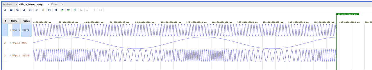
6. Minized Microphone Input PDM to PCM via Decimation
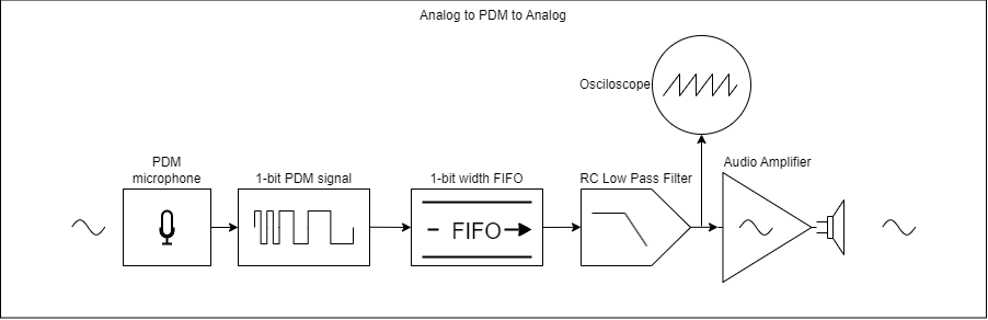
The MEMS microphone on the Minized development board captures sound and generates a 1-bit Pulse Density Modulated (PDM) signal. The signal is passed to a FIFO memory that will produce a small delay, the full flag signal is connected to the ready flag for reading. The output of the FIFO is still a PDM signal that is connected to a very simple DAC consisting of a simple low-pass RC filter.
6.1. Interfacing the MiniZed built-in microphone
The Avnet Minized development board has as its sound sensor an ST MP45DT02 MEMS microphone that generates a 1-bit pulse density modulated (PDM) signal. Pulse Density Modulation (PDM), is used in the representation and conversion of analog signals to the digital domain (and vice versa). The amplitude of the signals is represented by the relative density or number of pulses as a function of time. A one-bit stream is unacceptably noisy, but very high sampling rates and noise-shaping techniques are used to greatly reduce the noise in the audio spectrum. This noise energy is moved from the audio baseband into the area of the spectrum above 20 kHz, where it is inaudible.
The Pulse Code Modulation (PCM) is a modulation procedure used to transform an analog signal into a sequence of bits (digital signal), It is the standard form of digital audio in computers, compact discs, digital telephony, and other similar applications. In a PCM stream, the amplitude of an analog signal is sampled regularly at uniform intervals, and each sample is quantized to the nearest value within a range of digital steps.
The sound sensor on the MiniZed is hard configured as data valid on clock low.
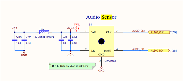
It is needed a slow clock for the MEMS microphone, in the range between 1.2 MHz and 3.25 MHz
The Vivado LogicCore Clock Wizard IP cannot generate clocks under 5MHz so it implemented a modulo-M counter with M equal to (input frequency / desired frequency)/2 to generate a 2.400 MHz clock signal from a 100 MHz clock signal.
Microphone clock generation
module pdm_clk_gen
  #(
    parameter INPUT_FREQ = 100000000,
    parameter OUTPUT_FREQ = 2400000

    )
   (
    input  clk,
    input  reset,
    output mic_clk,
    output clk_rising
    );

   logic   clk_rising_reg;
   logic   mic_clk_reg;

   localparam CLK_DIVIDER = INPUT_FREQ/OUTPUT_FREQ;

   // M-bit counter  M = LOG2(CLK_DIVIDER)
   logic [$clog2(CLK_DIVIDER)-1:0] clk_counter_reg;

   always_ff@(posedge clk) begin
      if (reset) begin
         clk_counter_reg    <= 0;
         mic_clk_reg    <= 0;
         clk_rising_reg <= 0;
      end
      else begin
         clk_rising_reg <= 0;
         if (clk_counter_reg < (CLK_DIVIDER/2)-1) begin
            clk_counter_reg <= clk_counter_reg + 1;
         end
         else begin
            clk_counter_reg    <= 0;
            mic_clk_reg        <= ~mic_clk_reg;
            clk_rising_reg     <= ~mic_clk_reg;

         end
      end
   end

   assign mic_clk = mic_clk_reg; // Microphone clock signal
   assign clk_rising = clk_rising_reg; //  output pulse on the rising edge of the clock for s_axis_data_tvalid


endmodule
In the Zynq hardware integrated logic analyzer (ILA IP) image capture we can see the 1-bit PDM output signal of the MEMS microphone and the signal output delayed by the FIFO.
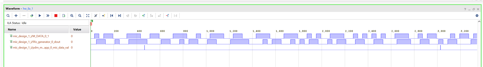
6.2. Checking Microphone capture
The video showcases the MiniZed development board's microphone, which produces a 1-bit PDM pulse density modulated signal. This signal is saved in a FIFO queue and transmitted to an output on the MiniZed, which is connected to a board with a low pass filter and amplifier. The data was captured using the Digilent waveforms program. The Digilent Analog Discovery 2 USB Oscilloscope was used for data acquisition.
6.3. PDM to PCM using the VIVADO CIC Compiler IP
A signal that is coded as PDM can be converted to PCM by sampling it at a lower rate (decimating) and increasing the word length. The ratio of the PDM bit rate to the decimated PCM sample rate is called the oversampling ratio. The decimation (also called "down-sampling") operation, means discarding all but every Rth sample.
Vivado includes a Cascaded Integrator Comb (CIC) Compiler. The Cascaded Integrator Comb (CIC) Compiler provides the ability to design and implement AXI4-Stream-compliant cascaded
integrator-comb (CIC) filters. https://docs.xilinx.com/v/u/en-US/pg140-cic-compiler
To make the PDM to PCM conversion we need to establish our design requirements. Our PDM input sample rate is 2.400 MHz and we want a PCM output sample rate of 48kHz.That is a decimation rate of 50.
The frequency response of the MP34DT05-A microphone of the MiniZed is only flat between 100Hz and 4.5kHz, after which it starts going up. So set the pass band filter specification from 0 to 6 kHz and the stop band to 10kHz.
Other requirements can be the passband ripple and the stop band attenuation for that we need to study the acoustic characteristics of our microphone.
6.4. Cascading Integrating Comb Filter
Cascaded Integrator-Comb (CIC) filters, also known as Hogenauer filters, are implementations of narrowband lowpass filters. These multi-rate filters are typically employed in applications where the system sample rate is much larger than the bandwidth occupied by the processed signal as in digital down converters (DDC). Compared to standard FIR filters, they are more economical since they do not include multipliers and use limited storage components. CIC uses only adders, subtracters, and delay elements.
In a decimating CIC, the input signal is fed through one or more cascaded integrators, then a down-sampler, followed by one or more comb sections (equal in number to the number of integrators). CIC is well suited for antialiasing filtering before decimation or sample rate reduction.
6.5. Configuration of the AMD LogiCORE IP CIC Compiler
The AMD LogiCORE IP CIC Compiler core provides the ability to design and implement AXI4-Stream-compliant cascaded integrator-comb (CIC) filters.
The Minized Synth uses a Decimation Filter with 5 stages, one channel, and a 50 rate change factor.
| {gallery}CIC COMPILER CONFIGURATION FOR PDM TO PCM VIA DECIMATION |
|---|
|
FILTER OPTIONS: Decimation, 5 stages, 50 Fixed Sample Rate, 100MHz Oversampling sample clock frequency, 2.4MHz input Sample Frequency |
|
IMPLEMENTATION OPTIONS: 16 bits output via truncation, input data width 2 |
|
CIC COMPILER: SUMMARY |
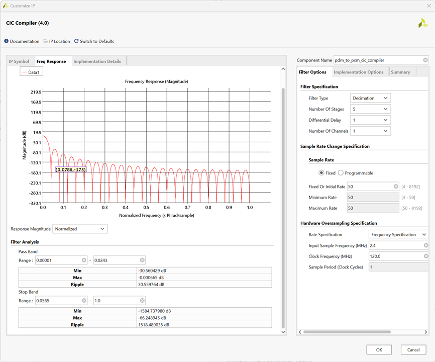

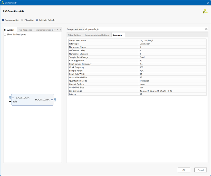
CIC Compiler Configuration
7. Indicator LEDs and Control Switches Auxiliary Expansion Board

This extension board with user buttons and indicator LEDs is configured as follows:
- The first button selects a Sawtooth (LED OFF) or Square wave (LED ON) for OSC 1.
- The second button selects a Sawtooth (LED OFF) or Square wave (LED ON) for OSC 2.
- The third button sets the input source level of NOISE (LED OFF) or MIC LED ON)
- Forth button enables or disables the Release segment of both Envelope Generators. When enabled, the Envelope Release time is the same as the Envelope Decay time, and the DECAY control adjusts the time for both segments. When disabled, the Release segment does not occur and the Envelope stops abruptly in response to a “Note Off” message (or when the Gate goes to zero).
This board has been built by soldering the components on a protoboard. The switches work in negative logic and have 1 KOhm SMD pull-up resistors, and the LEDs work with positive logic and have 10 KOhm SMD resistors to limit the current and therefore the intensity of the LED light.


Auxiliary board for the support of control switches and indicator LEDs.
The schematic is made with Easy EDA, so far I have not created a specific PCB for this module.

Schematic for the button panel of the control module and indicators made with EasyEDA.
The module needs 13 ports for inputs and outputs. 12 of the ports are taken from one of the PMOD connectors. The xdc configuration file allows you to use any of the two PMOD connectors on the MiniZed board. The thirteenth connects to one of the free ports on the Arduino connectors.
PMOD 1
| FUNCTION | PMOD1 PIN | DIRECTION | LOGIC | ZYNQ PACKAGE PIN | ZYNQ PACKAGE PIN | LOGIC | DIRECTION | PMOD1 PIN | Function | |
| LED5 | 7 | OUTPUT | POSITIVE | K13 | | | L15 | NEGATIVE | INPUT | 1 | SW1 |
| LED4 | 8 | OUTPUT | POSITIVE | L13 | M15 | NEGATIVE | INPUT | 2 | SW2 | |
| LED3 | 9 | OUTPUT | POSITIVE | N13 | L14 | NEGATIVE | INPUT | 3 | SW3 | |
| LED2 | 10 | OUTPUT | POSITIVE | N14 | M14 | NEGATIVE | INPUT | 4 | SW1 | |
| GND | 11 | GND | GND | 5 | GND | |||||
| VCC | 12 | 3V3 | 3V3 | 6 | VCC |
ARDUINO HEADERS
| FUNCTION | ARDUINO PIN | DIRECTION | LOGIC | ZYNQ PACKAGE PIN |
| LED1 | IO11 | OUTPUT | POSITIVE | M11 |
Constraints File
# Analog input VAUX0
set_property IOSTANDARD LVCMOS33 [get_ports Vaux0_0_v_n]
set_property IOSTANDARD LVCMOS33 [get_ports Vaux0_0_v_p]
# Analog input
set_property PACKAGE_PIN E13 [get_ports Vaux0_0_v_n]

# Analog input VAUX8
set_property IOSTANDARD LVCMOS33 [get_ports Vaux8_0_v_n]
set_property IOSTANDARD LVCMOS33 [get_ports Vaux8_0_v_p]


## ARDUINO IO10
set_property IOSTANDARD LVCMOS33 [get_ports {muxaddr_out_0[2]}]
set_property PACKAGE_PIN M10 [get_ports {muxaddr_out_0[2]}]


## ARDUINO IO9
set_property IOSTANDARD LVCMOS33 [get_ports {muxaddr_out_0[1]}]
set_property PACKAGE_PIN N9 [get_ports {muxaddr_out_0[1]}]

## ARDUINO IO8
set_property IOSTANDARD LVCMOS33 [get_ports {muxaddr_out_0[0]}]
set_property PACKAGE_PIN M9 [get_ports {muxaddr_out_0[0]}]


########################################################################
## Pmod #1 LEDs & SWITCHES
########################################################################

## PIN 1 - SW4 - SYNTH_SWITCHES_tri_i[3]
set_property IOSTANDARD LVCMOS33 [get_ports {SYNTH_SWITCHES_tri_i[3]}]
set_property PACKAGE_PIN L15 [get_ports {SYNTH_SWITCHES_tri_i[3]}]

## PIN 2 - SW3 - SYNTH_SWITCHES_tri_i[2]
set_property IOSTANDARD LVCMOS33 [get_ports {SYNTH_SWITCHES_tri_i[2]}]
set_property PACKAGE_PIN M15 [get_ports {SYNTH_SWITCHES_tri_i[2]}]

## PIN 3 - SW2 - SYNTH_SWITCHES_tri_i[1]
set_property IOSTANDARD LVCMOS33 [get_ports {SYNTH_SWITCHES_tri_i[1]}]
set_property PACKAGE_PIN L14 [get_ports {SYNTH_SWITCHES_tri_i[1]}]

## PIN 4 - SW1 -  SYNTH_SWITCHES_tri_i[0]
set_property IOSTANDARD LVCMOS33 [get_ports {SYNTH_SWITCHES_tri_i[0]}]
set_property PACKAGE_PIN M14 [get_ports {SYNTH_SWITCHES_tri_i[0]}]

## PIN 7 - LED2 - SYNTH_LEDS_tri_o[1]
set_property IOSTANDARD LVCMOS33 [get_ports {SYNTH_LEDS_tri_o[1]}]
set_property PACKAGE_PIN K13 [get_ports {SYNTH_LEDS_tri_o[1]}]

## PIN 8 - LED3 - SYNTH_LEDS_tri_o[2]
set_property IOSTANDARD LVCMOS33 [get_ports {SYNTH_LEDS_tri_o[2]}]
set_property PACKAGE_PIN L13 [get_ports {SYNTH_LEDS_tri_o[2]}]

## PIN 9 - LED4 - SYNTH_LEDS_tri_o[3]
set_property IOSTANDARD LVCMOS33 [get_ports {SYNTH_LEDS_tri_o[3]}]
set_property PACKAGE_PIN N13 [get_ports {SYNTH_LEDS_tri_o[3]}]

## PIN 9 - LED5 - SYNTH_LEDS_tri_o[4]
set_property IOSTANDARD LVCMOS33 [get_ports {SYNTH_LEDS_tri_o[4]}]
set_property PACKAGE_PIN N14 [get_ports {SYNTH_LEDS_tri_o[4]}]

########################################################################
### ARDUINO IO11  - LED1 - SYNTH_LEDS_tri_o[0]
########################################################################


set_property IOSTANDARD LVCMOS33 [get_ports {SYNTH_LEDS_tri_o[0]}]
set_property PACKAGE_PIN M11 [get_ports {SYNTH_LEDS_tri_o[0]}]

set_property C_CLK_INPUT_FREQ_HZ 300000000 [get_debug_cores dbg_hub]
set_property C_ENABLE_CLK_DIVIDER false [get_debug_cores dbg_hub]
set_property C_USER_SCAN_CHAIN 1 [get_debug_cores dbg_hub]
connect_debug_port dbg_hub/clk [get_nets clk]
8. Low Pass Filter and Sound Amplifier Expansion Boards

8.1. Analog RC Low Pass Filter
A simple passive RC low-pass filter is used as a digital-to-analog converter.
- Resistance 3.3 kΩ
- Capacitance 0.0047 µF
- -3dB Cutoff Frequency 10 kHz
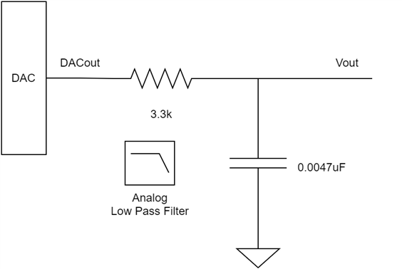
8.2 Sound Amplifier Expansion Board
The audio output connects to a commercially available LM386 audio amplifier.

9. Multiplexer Expansion Board
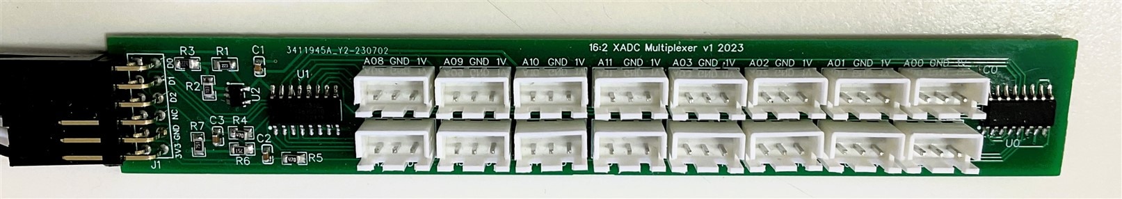
The MiniZed Synth needs to read the values of 16 analog potentiometers but the Avnet Minized board only exposes 4 channels of the Zynq's integrated analog-to-digital converter (XADC). This section presents the board that I have designed and built to obtain the reading of the 16 analog potentiometers that are included in the control panel for sound editing.
Zynq's XADC allows the use of an external analog multiplexer to implement several external analog inputs in situations where FPGA I/O resources are limited and auxiliary analog inputs are not available as is our case. A 16:2 Multiplexer Expansion Board is designed and built for the project.

Custom-made XADC 16:2 External Multiplexer addon board for the MiniZed
An analog-to-digital converter (ADC) is a circuit that digitizes a continuous analog signal by converting its voltage level to a discrete digital quantity. The AMD Zynq-700 SoC and the AMD Xilinx FPGA 7 series have an integrated analog-to-digital converter (XADC). The XADC has two 12-bit 1 mega samples per second (MSPS) ADCs with separate track and hold amplifiers, an analog multiplexer (up to 17 external analog input channels), and on-chip thermal and on-chip voltage sensors. The two ADCs can be configured to simultaneously sample two external-input analog channels.
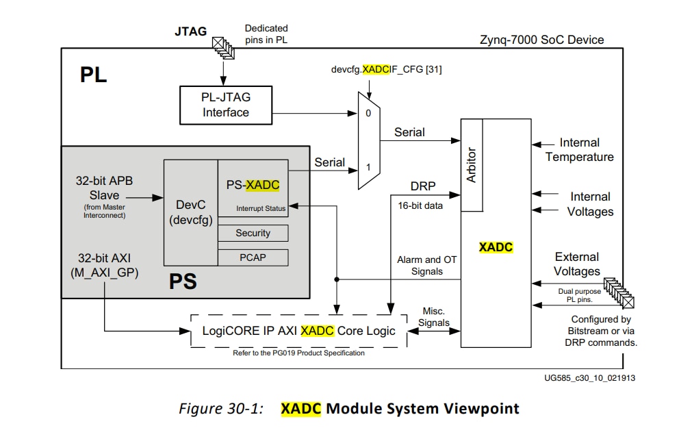
The XADC can read up to 17 analog channels in sequence but the Avnet MiniZed board only exposes 4 channels of the integrated analog-to-digital converter (XADC).
9.1. AMD XADC External Multiplexer Mode
Fortunately, the XADC supports the use of an external analog multiplexer to implement several external analog inputs in situations where FPGA I/O resources are limited and auxiliary analog inputs are not available.
The XADC track/hold amplifiers return to track mode as soon as a conversion starts. Therefore, the acquisition on the next channel can start during the current conversion cycle. An output bus called MUXADDR[4:0] allows the XADC to control an external multiplexer.
The address on this bus reflects the channel currently being acquired, and it changes state as soon as the XADC enters acquisition mode. Users can also nominate the channel to be used with an external multiplexer.
The designed board takes advantage of the external multiplexer mode in simultaneous sampling mode.
9.2. External Multiplexer mode in simultaneous sampling mode
In the case of simultaneous sampling mode, two channels must be allocated to two external multiplexers to support simultaneous sampling.
The next figure illustrates how the external multiplexer mode is implemented for simultaneous sampling mode. The channels selected for connection are also selected by writing to CH4 to CH0 but are allocated in pairs. For example, writing 16 ( 10000 ) to CH4 to CH0 would select auxiliary channels 0 and 8 for connection to external multiplexers as shown in the figure.
When placed in simultaneous sampling mode, the sequencer automatically sequences through eight pairs of auxiliary analog input channels for simultaneous sampling and conversion.
This is the mode I have chosen for the design of the multiplexer. The 16:2 multiplexer takes advantage of the simultaneous reading performed by the two ADC converters of the XADC module.
XADC Channels assignment
9.3. External Multiplexer Circuit Design
DISCLAIMER: I am not an electrical engineer, just a hobbyist, use at your own risk. The design is working correctly for me and it's doing its job.
The expansion board use two 74HC4051D,653-Analog Multiplexer / Demultiplexer, 8:1
The 74HC4051 is a single-pole octal-throw analog switch (SP8T) suitable for use in analog or digital 8:1 multiplexer/demultiplexer applications. The switch features three digital select inputs (S0, S1, and S2), eight independent inputs/outputs (Yn), a common input/output (Z), and a digital enable input (E). When E is HIGH, the switches are turned off.

74HC4051,single-pole octal-throw analog switch (SP8T)
The addresses for the external multiplexer go from 0 to 7, and three XADC multiplexer output signals (D0, D1, D2) address the 8 analog inputs for both independent 8:1 multiplexers.
The board limits the analog signal to 1V using a buffered voltage divider.

Those headers are for connecting up to 16x10K potentiometers.

The double-sided PCB is designed with easyEDA. I had never ordered a circuit from an online service before, it has been a new experience for me.
16:2 Multiplexer Expansion Board PCB
| {gallery}XADC 16:2 Multiplexer PCB |
|---|
|
|
|
|
|
|
|
|
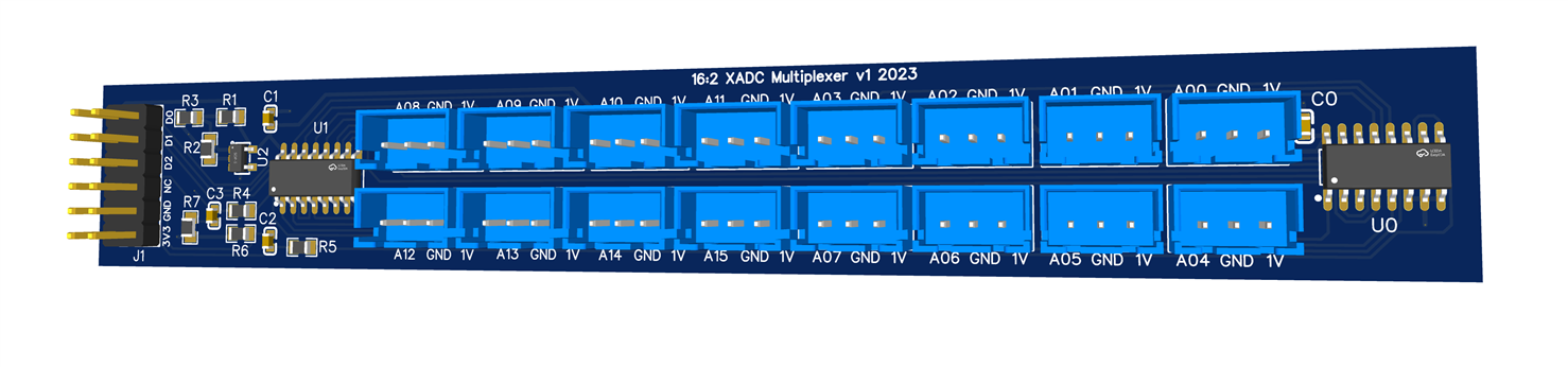


The project in easyEDA json format:
PCB_PCB_ADCMultiplexerV3_2023-07-02.zip
Gerber_PCB_ADCMultiplexerV3.zip
9.4. 16:2 Multiplexer Expansion Board Bill of Materials
| Product Name | Manufacturer | Quantity | Buy Kit |
|---|---|---|---|
| M20-9740642-Pin Header, Board-to-Board, 2.54 mm, 2 Rows, 12 Contacts, Through Hole Right Angle, M20 | HARWIN | 1 | Buy Now |
| C0603C104K5RACAUTO-SMD Multilayer Ceramic Capacitor, AEC-Q200, 0.1 µF, 50 V, 0603 [1608 Metric], ± 10%, X7R | KEMET | 2 | Buy Now |
| B3B-XH-A (LF)(SN)-Pin Header, Vertical, Wire-to-Board, 2.5 mm, 1 Rows, 3 Contacts, Through Hole Straight, XH | JST (JAPAN SOLDERLESS TERMINALS) | 16 | Buy Now |
| CRCW060322K0FKEA-SMD Chip Resistor, 22 kohm, ± 1%, 100 mW, 0603 [1608 Metric], Thick Film, General Purpose | VISHAY | 1 | Buy Now |
| CRCW080510K0FKEA-SMD Chip Resistor, 10 kohm, ± 1%, 125 mW, 0805 [2012 Metric], Thick Film, General Purpose | VISHAY | 1 | Buy Now |
| CRCW0805220KFKEA-SMD Chip Resistor, 220 kohm, ± 1%, 125 mW, 0805 [2012 Metric], Thick Film, General Purpose | VISHAY | 1 | Buy Now |
| 74HC4051D,653-Analog Multiplexer / Demultiplexer, 8:1, 1 Circuit, 2V to 10V, SOIC-16 | NEXPERIA | 2 | Buy Now |
| LMV321SN3T1G-Operational Amplifier, RR O/P, 1 Amplifier, 1 MHz, 1 V/µs, 2.7V to 5V, TSOP, 5 Pins | ONSEMI | 1 | Buy Now |
| {gallery}XADC 16:2 External Multiplexer Expansion Board |
|---|
|
|
|
|
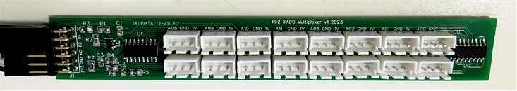
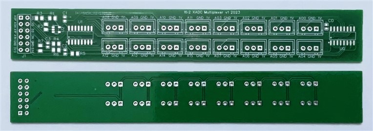

The form factor allows the board to be used in a PMOD connector.
XADC Channels assignment
The following diagram shows the XADC channel assignment to each of the analog potentiometers on the front panel.
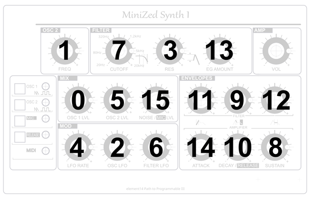
Function Assignment to XADC Channels Diagram
Function Assignment to XADC Channels
| XADC Channel | Function |
| A00 | OSC1 LVL |
| A01 | LFO RATE |
| A02 | OSC LFO |
| A03 | LFO FILTER |
| A04 | OSC2 FREQ |
| A05 | OSC2 LVL |
| A06 | FILTER RES |
| A07 | FILTER CUTOFF |
| A08 | AMP ENVELOPE SUSTAIN |
| A09 | FILTER ENVELOPE SUSTAIN |
| A10 | AMP ENVELOPE DECAY/RELEASE |
| A11 | AMP ENVELOPE ATTACK |
| A12 | FILTER ENVELOPE DECAY |
| A13 | FILTER EG AMOUNT |
| A14 | FILTER ENVELOPE ATTACK |
| A15 | NOISE / MIC LVL |
9.5. XADC IP Configuration
The XADC is configured for simultaneous sampling with an external multiplexer, using the AXI4Lite interface for control in continuous mode and using channel averaging as a low pass filter.
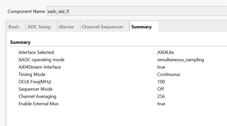
VIVADO XADC Wizard configuration summary
VIVADO XADC IP CONNECTION
The Vivado block diagram shows how the XADC IP module is connected to the Zynq processor.
Two Integrated Logic Analyzers have been added, one to sample the output of the multiplexer router and another to monitor the communication on the AXI bus.

Constraints file
# Analog input VAUX0
set_property IOSTANDARD LVCMOS33 [get_ports Vaux0_0_v_n]
set_property IOSTANDARD LVCMOS33 [get_ports Vaux0_0_v_p]
# Analog input
set_property PACKAGE_PIN E13 [get_ports Vaux0_0_v_n]

# Analog input VAUX8
set_property IOSTANDARD LVCMOS33 [get_ports Vaux8_0_v_n]
set_property IOSTANDARD LVCMOS33 [get_ports Vaux8_0_v_p]


## ARDUINO IO10
set_property IOSTANDARD LVCMOS33 [get_ports {muxaddr_out_0[2]}]
set_property PACKAGE_PIN M10 [get_ports {muxaddr_out_0[2]}]


## ARDUINO IO9
set_property IOSTANDARD LVCMOS33 [get_ports {muxaddr_out_0[1]}]
set_property PACKAGE_PIN N9 [get_ports {muxaddr_out_0[1]}]

## ARDUINO IO8
set_property IOSTANDARD LVCMOS33 [get_ports {muxaddr_out_0[0]}]
set_property PACKAGE_PIN M9 [get_ports {muxaddr_out_0[0]}]


########################################################################
## Pmod #1 LEDs & SWITCHES
########################################################################

### PIN 1 - SW4 - SYNTH_SWITCHES_tri_i[3]
#set_property IOSTANDARD LVCMOS33 [get_ports {SYNTH_SWITCHES_tri_i[3]}]
#set_property PACKAGE_PIN L15 [get_ports {SYNTH_SWITCHES_tri_i[3]}]

### PIN 2 - SW3 - SYNTH_SWITCHES_tri_i[2]
#set_property IOSTANDARD LVCMOS33 [get_ports {SYNTH_SWITCHES_tri_i[2]}]
#set_property PACKAGE_PIN M15 [get_ports {SYNTH_SWITCHES_tri_i[2]}]

### PIN 3 - SW2 - SYNTH_SWITCHES_tri_i[1]
#set_property IOSTANDARD LVCMOS33 [get_ports {SYNTH_SWITCHES_tri_i[1]}]
#set_property PACKAGE_PIN L14 [get_ports {SYNTH_SWITCHES_tri_i[1]}]

### PIN 4 - SW1 -  SYNTH_SWITCHES_tri_i[0]
#set_property IOSTANDARD LVCMOS33 [get_ports {SYNTH_SWITCHES_tri_i[0]}]
#set_property PACKAGE_PIN M14 [get_ports {SYNTH_SWITCHES_tri_i[0]}]

### PIN 7 - LED2 - SYNTH_LEDS_tri_o[1]
#set_property IOSTANDARD LVCMOS33 [get_ports {SYNTH_LEDS_tri_o[1]}]
#set_property PACKAGE_PIN K13 [get_ports {SYNTH_LEDS_tri_o[1]}]

### PIN 8 - LED3 - SYNTH_LEDS_tri_o[2]
#set_property IOSTANDARD LVCMOS33 [get_ports {SYNTH_LEDS_tri_o[2]}]
#set_property PACKAGE_PIN L13 [get_ports {SYNTH_LEDS_tri_o[2]}]

### PIN 9 - LED4 - SYNTH_LEDS_tri_o[3]
#set_property IOSTANDARD LVCMOS33 [get_ports {SYNTH_LEDS_tri_o[3]}]
#set_property PACKAGE_PIN N13 [get_ports {SYNTH_LEDS_tri_o[3]}]

### PIN 9 - LED5 - SYNTH_LEDS_tri_o[4]
#set_property IOSTANDARD LVCMOS33 [get_ports {SYNTH_LEDS_tri_o[4]}]
#set_property PACKAGE_PIN N14 [get_ports {SYNTH_LEDS_tri_o[4]}]


########################################################################
## Pmod #2 LEDs & SWITCHES
########################################################################

## PIN 1 - SW4 - SYNTH_SWITCHES_tri_i[3]
set_property IOSTANDARD LVCMOS33 [get_ports {SYNTH_SWITCHES_tri_i[3]}]
set_property PACKAGE_PIN P13 [get_ports {SYNTH_SWITCHES_tri_i[3]}]

## PIN 2 - SW3 - SYNTH_SWITCHES_tri_i[2]
set_property IOSTANDARD LVCMOS33 [get_ports {SYNTH_SWITCHES_tri_i[2]}]
set_property PACKAGE_PIN P14 [get_ports {SYNTH_SWITCHES_tri_i[2]}]

## PIN 3 - SW2 - SYNTH_SWITCHES_tri_i[1]
set_property IOSTANDARD LVCMOS33 [get_ports {SYNTH_SWITCHES_tri_i[1]}]
set_property PACKAGE_PIN N11 [get_ports {SYNTH_SWITCHES_tri_i[1]}]

## PIN 4 - SW1 -  SYNTH_SWITCHES_tri_i[0]
set_property IOSTANDARD LVCMOS33 [get_ports {SYNTH_SWITCHES_tri_i[0]}]
set_property PACKAGE_PIN N12 [get_ports {SYNTH_SWITCHES_tri_i[0]}]

## PIN 7 - LED2 - SYNTH_LEDS_tri_o[1]
set_property IOSTANDARD LVCMOS33 [get_ports {SYNTH_LEDS_tri_o[1]}]
set_property PACKAGE_PIN P15 [get_ports {SYNTH_LEDS_tri_o[1]}]

## PIN 8 - LED3 - SYNTH_LEDS_tri_o[2]
set_property IOSTANDARD LVCMOS33 [get_ports {SYNTH_LEDS_tri_o[2]}]
set_property PACKAGE_PIN R15 [get_ports {SYNTH_LEDS_tri_o[2]}]

## PIN 9 - LED4 - SYNTH_LEDS_tri_o[3]
set_property IOSTANDARD LVCMOS33 [get_ports {SYNTH_LEDS_tri_o[3]}]
set_property PACKAGE_PIN R12 [get_ports {SYNTH_LEDS_tri_o[3]}]

## PIN 9 - LED5 - SYNTH_LEDS_tri_o[4]
set_property IOSTANDARD LVCMOS33 [get_ports {SYNTH_LEDS_tri_o[4]}]
set_property PACKAGE_PIN R13 [get_ports {SYNTH_LEDS_tri_o[4]}]

########################################################################
### ARDUINO IO11  - LED1 - SYNTH_LEDS_tri_o[0]
########################################################################


set_property IOSTANDARD LVCMOS33 [get_ports {SYNTH_LEDS_tri_o[0]}]
set_property PACKAGE_PIN M11 [get_ports {SYNTH_LEDS_tri_o[0]}]

########################################################################
### PDM MICROPHONE
########################################################################

### MiniZed Microphone CLK
set_property PACKAGE_PIN L12 [get_ports AUDIO_CLK]
set_property IOSTANDARD LVCMOS33 [get_ports AUDIO_CLK]

### MiniZed Microphone DAT
set_property PACKAGE_PIN M12 [get_ports AUDIO_DAT]
set_property IOSTANDARD LVCMOS33 [get_ports AUDIO_DAT]

## AUDIO OUT ARDUINO ARDUINO_IO12
set_property IOSTANDARD LVCMOS33 [get_ports {AUDIO_OUT}]
set_property PACKAGE_PIN R11 [get_ports {AUDIO_OUT}]
In the image, the MinZed ports are used for the multiplexed reading of the 16 potentiometers according to the XDC constraints configuration file.
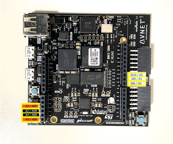
In the following video, you can see the data capture of 16 potentiometers made by multiplexing.
A small C program was made that runs in the Zynq processing system on the ARM A9 processor and that is polling the registers of the XADC module and sending the reading of the 16 channels through the serial port in CSV format. Reading the serial port is done using the Windows Serial Plot program.
The XADC module is configured to take an average of 256 readings, working this average as a very suitable low-pass filter for this type of reading with so much noise. It is also observed that the two channels are not symmetrical, this is because the Minized shares some of the ports with the output for the Programmable Logic LEDs and there is a slight voltage drop on one of the channels. This can be solved by cutting a track from the MiniZed but the current design solves it in software by adjusting the values using a map function.
10. ARM 9 Bare Metal Software App. MIDI Control
The full firmware is still unfinished. Below you can see a video with the main functions implemented that allow you to control the two main oscillators, the noise source and the detune.
Two of the buttons allow you to change the wave type of the two oscillators. Three potentiometers allow you to adjust the three input levels of the mixer. The third button changes the octave of the oscillators and adjusts the frequency of a note, and the fourth button releases the ADSR so you can continuously hear the pitch.
You can also adjust the rate of the low-frequency oscillator which affects the modulation of the frequency of the oscillators and the desired level of modulation. The output filter settings and MIDI communication are still pending development.
ATTENTION: The video is quite long, more than four minutes, and has very loud sounds, Turn down the volume and try not to use headphones.
Testing the Attack-Decay-Sustain-Releases envelops and the Low-Frequency Oscillators. MiniZed Synths plays a 4 octaves musical scale in different configurations of the oscillators, noise source, ADSR envelopes and LFOs.
The current version implements a simple variable cutoff frequency low-pass filter based on a moving average. At the moment it does not have a feedback loop for resonance. In the video you can see a frequency analysis of how the filter affects different waveform frequencies. The video has no sound.
Popcorn Melody
11. Creating the prototype
From idea to prototype. It has been many hours of design and discarding solutions. The most difficult thing has been defining the scope to be able to carry out the project in one month.
In the images some moments of the development of the project.
| {gallery}From idea to prototype |
|---|
|
MiniZed Synth Design: Cardboard prototype |
|
Learning communication between programmable logic and the processing system |
|
|
 |
 |
 |
|
Checking audio output section: RC Low-Pass Filter and LM386 sound amplifier. |
|
MiniZed Synth Design: Checking cable lengths |
|
MiniZed Synth 1: Components |
|
Control panel front: switches, LEDs, and pots |
|
|
|
Main boards connected: Exploded view |
|
|
|
|
|
Top view |
|
Checking the arrangement of modules. |


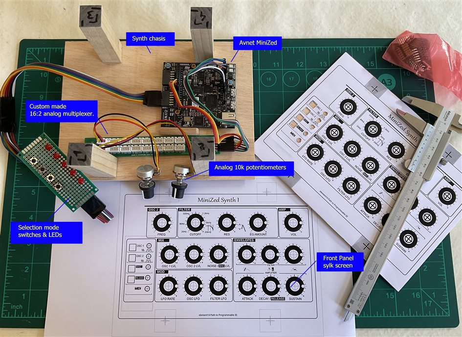
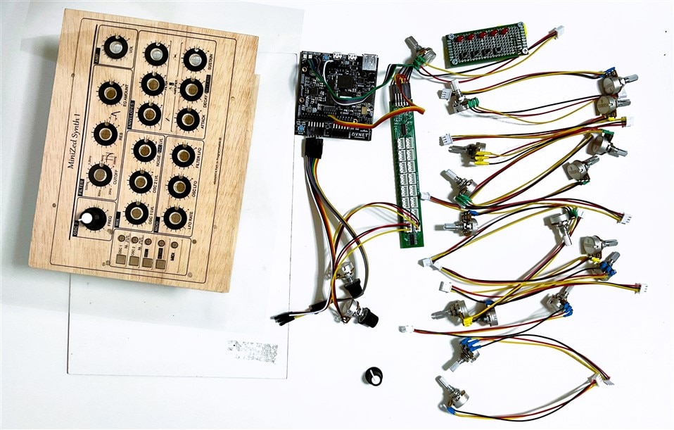
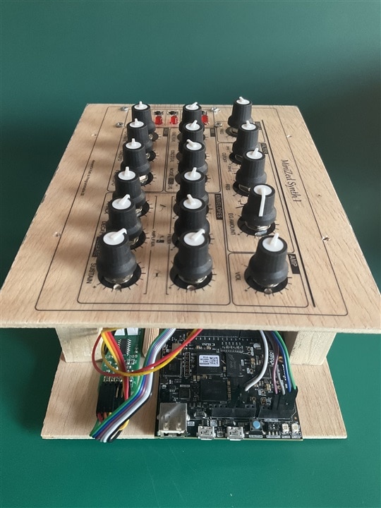
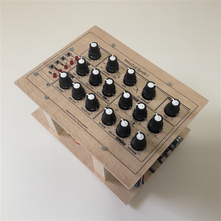
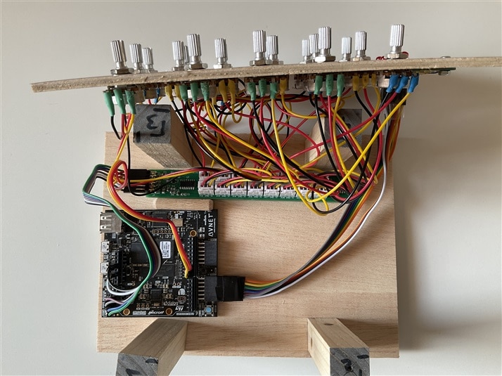
12. Code Repository and References
Github repository
https://github.com/javagoza/e14PathToProgrammableIII
References
Software Synthesis (basicsynth.com)
TFilter - Free online FIR filter design (engineerjs.com)
13. Conclusion and next steps
Throughout this project, I utilized all the skills that I acquired during my three-year time as a member of Element14. These abilities consist of composing technical blog posts in English, designing marquetry crafts, programming microcontrollers, creating digital circuits using HDL, constructing a PCB, and handling SMD components. While the latter two skills were unfamiliar to me, I have found them both enjoyable and challenging due to my limited experience and the brief length of this program.
Initially, I lacked knowledge about musical synthesizers and their functioning. However, I have managed to gain a better understanding through this project. I hope that the reader can also benefit from the information I have gathered.
I am extremely pleased with the results of this project, and I hope that it inspires others who, like me, have pursued electronics as a hobby despite coming from a different professional background.
The project is far from over as I still have numerous hours ahead to experiment and continue learning. Rest assured, I will keep sharing any new developments on Element14.
I want to express my gratitude to the amazing team at Element14 and sponsor AMD for allowing me to take part in the free training course on AMD's APSoC development tools, Vivado and Vitis IDE. I also want to give a shout-out to all the other participants in the training program for sharing their questions and insights in the forums. Thank you all!
14. Path to Programmable III Training Blog Series
You can access the entire series of blogs I have written for the "Path to Programmable III" program:
- BLOG 1: P2P3 Getting Started. Clockless Hardware Blinky on the Avnet Minized
- BLOG 2: P2P3 AMD Vitis portability and reuse. Migrating a Microblaze bare metal environmental monitor App to the Zynq architecture.
- BLOG 3: P2P3 AMD Zynq-7000 SoC XADC. External Multiplexer Mode.
- BLOG 4: P2P3 AMD Vivado Cascaded Integrator Comb (CIC) Compiler. PDM Microphone to PCM Decimation
- BLOG 5: P2P3 Wireless sensors on the Avnet Minized. Getting Started with PetaLinux
- FINAL PROJECT: AMD Zynq SoC MIDI Vintage Sound Synthesizer - Final


