Introduction
My goal in this project is to practice what I have learned in the training courses by creating a reference tutorial type project that starts from scratch and builds a simple but complete control system utilizing both PL and PS of the Zynq SoC on the MiniZed board. I have wished that the training course will walk me through a project like this, but it didn’t happen, so I decided to create this tutorial project myself.
Even though this is a competition and I know from my past experience with Element 14 design challenges that usually the most complex projects win, this time I decided not to necessarily focus on making a complex project that wins, but instead to make a simple tutorial project that may be a source of inspiration to a large number of “very beginners” who struggle to make their way through the complicated process of learning how to use SoC FPGAs.
I have been an engineer for the past 30 years and I have also been developing and teaching courses at UCLA Extension for the past 15 years, and I have always created courses that build the knowledge gradually on validated solid foundations like a pyramid structure. These Path to Programmable 3 training courses have been very intense and they have covered a lot of features of the Zynq 7000 SoC and a lot of features of the Vivado and Vitis design tools; however, it looks to me that the training courses have been developed by marketing or application engineers who have focused primarily on including as many features as possible but without structuring the courses from a "student" or “creator” perspective. A creator likes to build a project like a construction building starting with the foundation and adding layer by layer all the structures and features until the entire building is completed.
These Path to Programmable 3 training courses “drop” the student into the middle of a “knowledge storm” introducing multiple concepts in an “amalgam” format in which, if following the instructions correctly, everything magically falls into place and works as expected. This method works well for marketing presentations and demonstrations to potential customers. However, this method is very overwhelming for beginners and often makes them give up. I believe that this may be the one of the reasons why in this design challenge 30 out of 44 participants have dropped out. I hope that this tutorial project will inspire and bring back some of these participants into being interested in designing with Zynq SoC and the MiniZed board.
What I want to build in this tutorial project
In this tutorial project I have chosen to build a very simple temperature control system. Most of us are familiar with temperature control systems from the heating and air conditioning thermostats in our houses. We set a temperature that we want to have in the room and then a control system turns ON and OFF a heater and/or a cooler to maintain the temperature in the room as close as possible with the temperature that we have set up. In this project I will build a temperature control system implemented in both the PL and PS of the Zynq 7000 SoC on the Avnet MiniZed board. The temperature control system will use the MiniZed board and in addition it will use two push buttons for adjusting the programmed temperature up and down, a temperature sensor HTU21D that I have also used part of the training courses, a resistor as heating element, and a mini fan as cooling element. Here is a block diagram of the system that I will build.
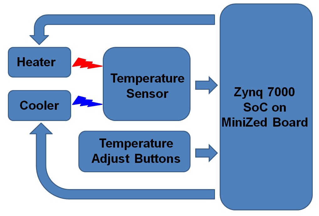
The functionality of this system can be “visually” described using the high level flowchart, shown below:
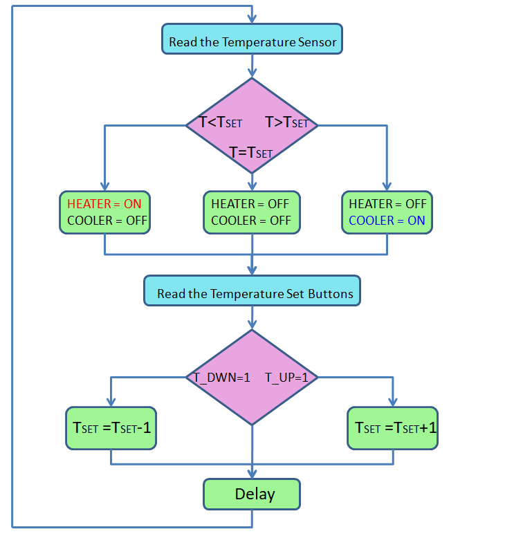
The system will be implemented as a continuous loop that periodically measures the room temperature, as illustrated in the first block at the top of the flowchart, then it compares the measured temperature with the set temperature, as illustrated in the diamond shape block following below the first block, and depending on the comparison result it will either turn on the heater, turn on the cooler, or turn or keep both heater and cooler off. Next, the control loop will check if the user has pressed any of the temperature adjust buttons, as illustrated in the light blue block labeled “Read Temperature Set Buttons”. If any of the buttons have been pressed then, as indicated in the next diamond shaped block, the set temperature is either incremented or decremented by one degree (one degree to keep it simple; a fraction of degree can also be used for finer resolution). The control loop will then pause for a defined delay time as illustrated in the block labeled “Delay” at the bottom of the flow chart. This delay is needed to keep the system stable, and experiments can be run to see what happens if the delay value is too short or too long.
This was a high level flowchart diagram used for a “first level” understanding on how this control system will work. However, for moving to the next step of implementation I need a more detailed flowchart that includes an initialization, defines the major variables, and adds a temperature comparison window since in reality the measured and set temperatures will be most of the times not equal, but close enough within an acceptable variation window. So next step I have developed a more detailed flowchart diagram, shown below:
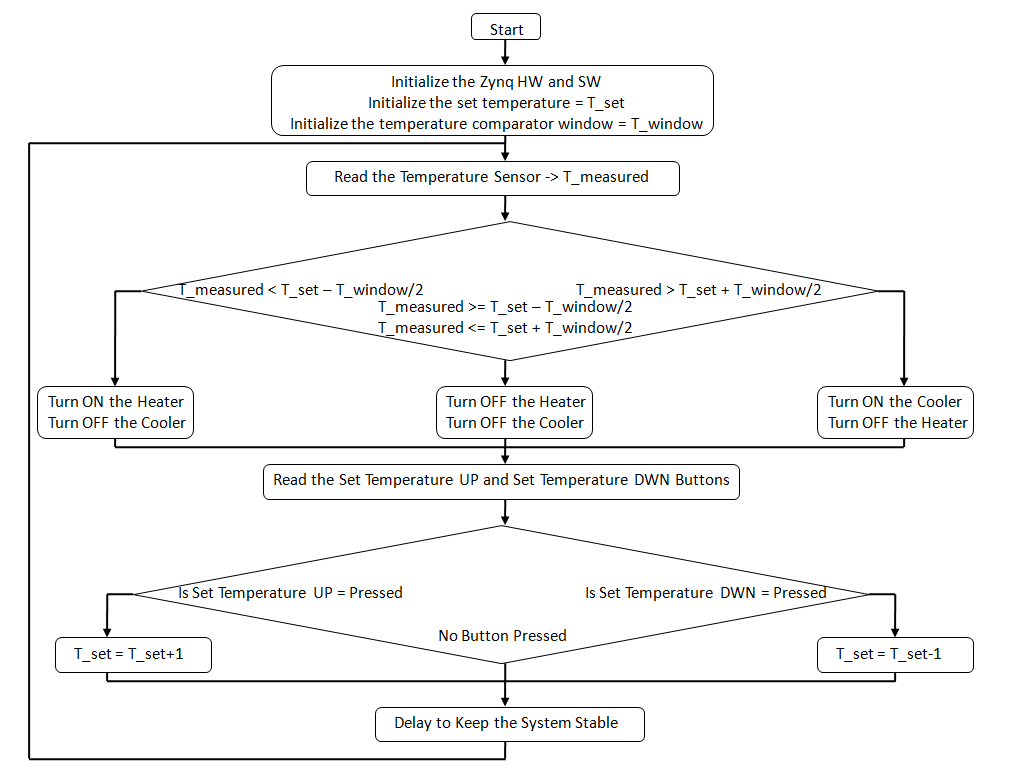
In this flowchart the system starts with initializing the Zynq SoC (memory, peripherals …), initializing the variables in the PS code, and then it starts a continuous (infinite) loop. The functionality of this loop is similar to what I have described in the simplified flowchart except now there is a temperature comparator window, T_window, so that if the measured temperature is within this T_window around the set temperature, the system will consider it “equal” to the set temperature and it will not activate the heater or the cooler.
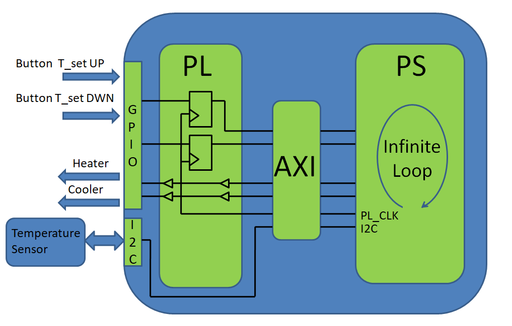
I will discuss now in more details the implementation of this system in the Zynq SoC. The Zync SoC has two major sections, a programmable logic (PL) section and a processing system (PS) section. The PL section can be programmed to be a logic electric circuit that once we configure it stays like that all the time until we power down the board (next power-up it is configured again as the Zynq SoC is re-programmed). The PS section is a microprocessor that executes a software code. The communication between PL and PS is done through a configurable hardware interface named AXI. So in this project I will have some of the functions implemented in the PL, and some in the PS. I will also configure the AXI interface to pass signals between the PL and PS. Here is a diagram showing the partition of the functions between the PS and PL.
So I am done with the project planning and now I will discuss the implementation plan. From my previous experience developing products, I have learned that if I put everything together and build the entire product without verifying anything in between, chances are that the product will not work on the first time and some troubleshooting will be needed. This can be quite disappointing, discouraging, and sometimes hard to handle especially in complicated systems. Often it may be overwhelming only to think of where in the system the problem or problems could be. To avoid this, my approach in building products is to divide the development in separate steps, each step being developed and verified before the next step is started. This way every time I start working on a step, what I have already built in the previous steps constitutes a proven “solid foundation” for the step that I am currently working on. With this approach in mind here is the plan that I am following for this project:
Project Development Steps:
Step 1 – Create a simple Zynq PL only project and test it in the lab
Goal: Build and verify the Zynq PL GPIO interface. This part consists of a mini-project built in Vivado that reads the temperature adjust buttons and drives two GPIO outputs. After this step the project will be compiled and programmed in the Zynq SoC on the MiniZed board. I will perform lab experiments on the programmed board.
Step 2 – Add some complexity to the Zynq PL only project and test it in the lab
Goal: After in step one I have validated that I can bring signals from “outside” to inside the Zynq SoC and I can drive signals from inside the Zynq SoC to the outside, in ”Step 2” mini-project I will add flip-flops in the Zynq PL to “store” the logic values that I read from the external push buttons. This step will still use only the PL of the Zynq SoC, so since in the MiniZed board there is no clock generator connected to the PL I will generate the clock to the flip-flop externally from one push button. At the end of this step I will compile the project and configure it in the Zynq SoC. I will then perform lab experiments to validate the functionality.
Step 3 – Introduce the Zynq PS in the project and test it in the lab
Goal: Now since I have built and validated the data read and flip-flop store functions implemented in the PL, I will add an internal clock signal to the flip-flops. The internal clock signal will be provided by the PS of the Zynq SoC. The PS receives an input clock signal from the MiniZed board, and I will configure the PS to distribute a “copy” of that clock to the PL. Since in this step I use the PS, I will have to export the hardware from Vivado into Vitis and I will need to compile the project and program the Zynq SoC from Vitis. When done wI will validate the functionality experimentally in the lab.
Step 4 – Introduce the AXI interface between PS and PL, write a simple C code in the PS, and test the project in the lab
Goal: In this step I will add the AXI communication interface between the PL and PS, and pass the temperature set buttons signals to PS through the AXI interface. I will also add two control signals for heater and cooler in the PS and route them to PL through the AXI interface. I will compile the project in Vitis and validate it experimentally in a lab experiment.
Step 5 – Develop the temperature control system project and test it in the lab
Goal: Now, after I have implemented and validated the project infrastructure in both PL and PS of the Zynq SoC, I will develop the temperature control software code that will execute in the Zynq PS. Outside the MiniZed board I will add the temperature sensor, the resistor heating element, and the mini fan cooling element. I will compile the project in Vitis and I will configure the Zynq SoC. I will then perform various experiments in the lab to validate the functionality.
So this is the plan; I am now starting with the first step:
Step 1
In step 1 I will use Vivado to build a PL GPIO interface that reads the temperature adjust buttons and drives two GPIO outputs for controlling the heater and the cooler of our temperature control system. In this step I will use two LEDs to verify that the heater and cooler GPIO signals are generated correctly. Later, I will add the actual heater and cooler devices. So I started by opening Vivado:

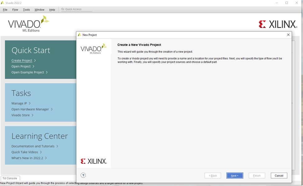
After it opened, I clicked on the option “Create Project” to create a new project space in which I will develop this temperature control system.
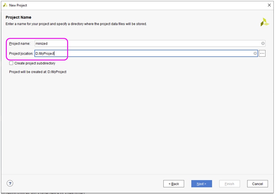
I have named this project “MiniZed”:
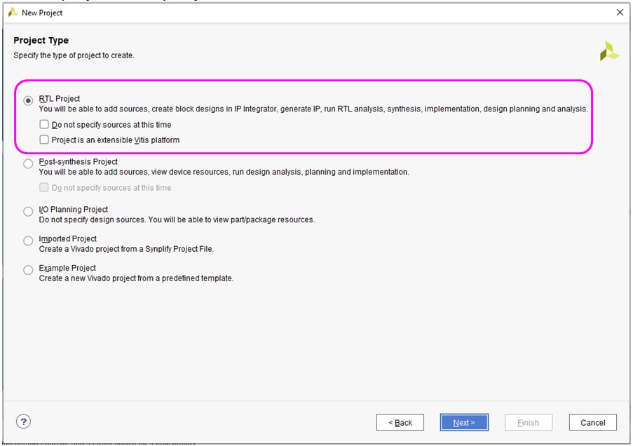
,and I have chosen “RTL Project” as project type:
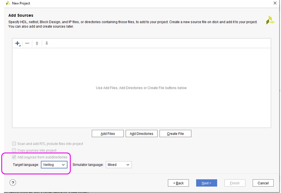
Next, the project setup asks to add sources to the project but I have skipped that step for that moment and I have also skipped the next one “Add Constraints” – I will come back to do this later after the project space is setup. Another decision to be made at this stage is to choose the HDL coding language. I have chosen Verilog for this project:
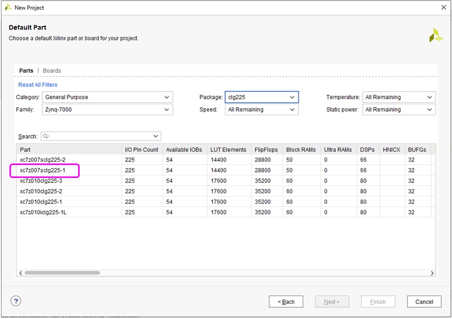
Next, it was the screen that selects the device part number, and for this MiniZed board I have selected the xc7z007sclg225-1, which corresponds to the Zynq SoC on my MiniZed board.
Then a project summary window shows the selections before confirming to create the project space.
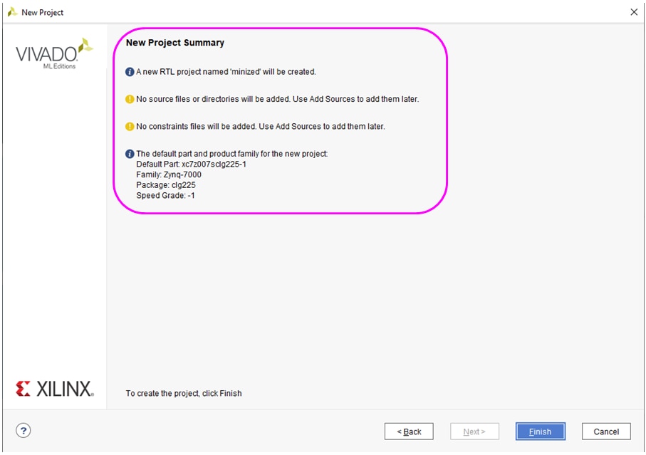
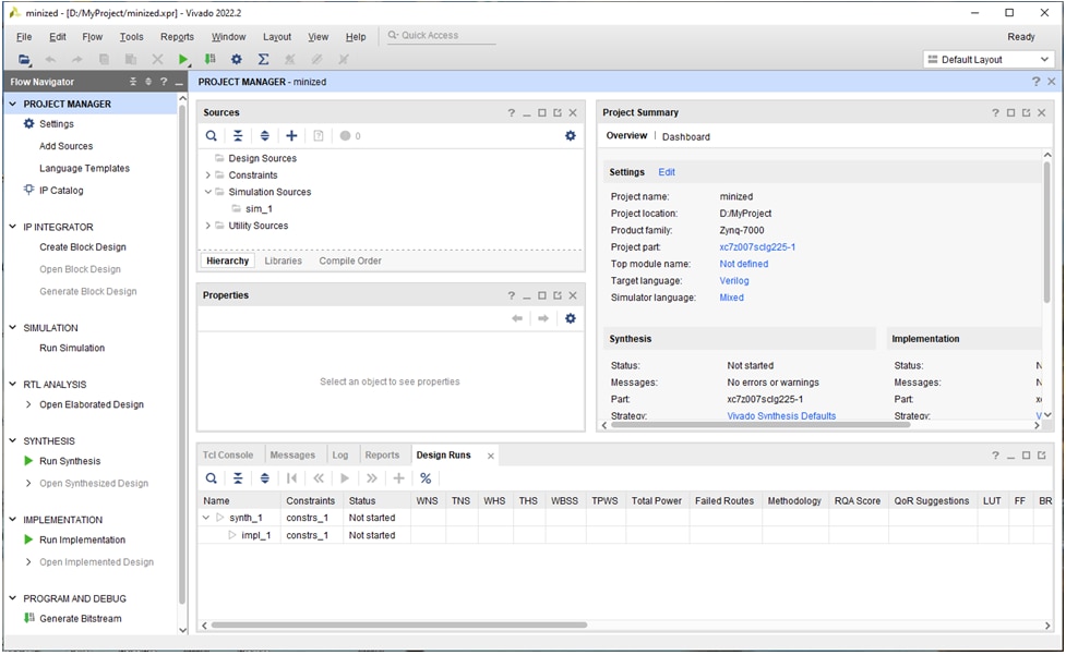
After I checked that all the entries were what I wanted, I clicked “Finish” and Vivado has then created the project workspace:
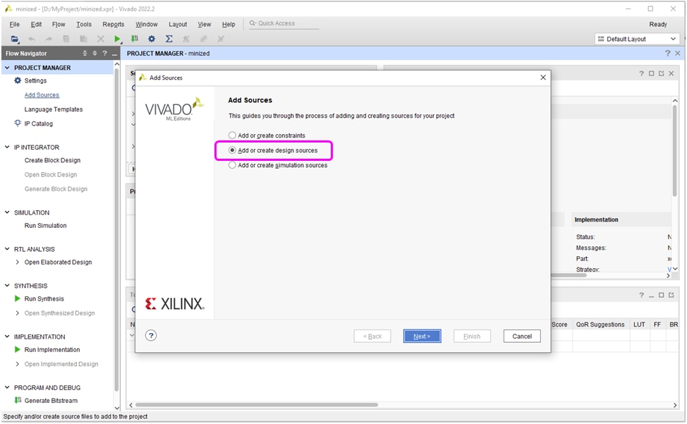
Next, I was ready to build the design for step 1, so I started by adding design sources:
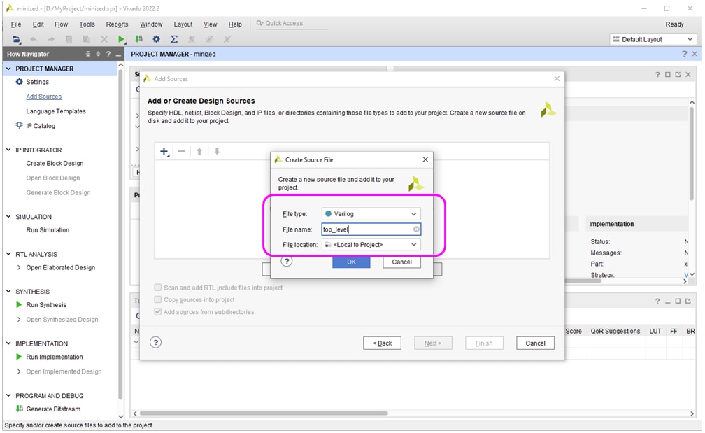
I named the source “top_level” and the file type was Verilog:
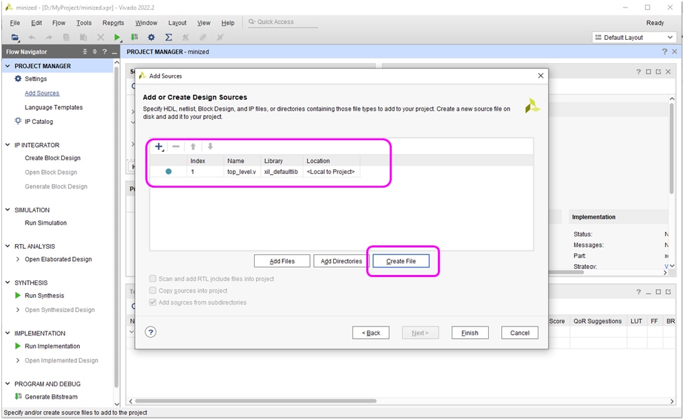
On the next screen I have clicked “Create File”.
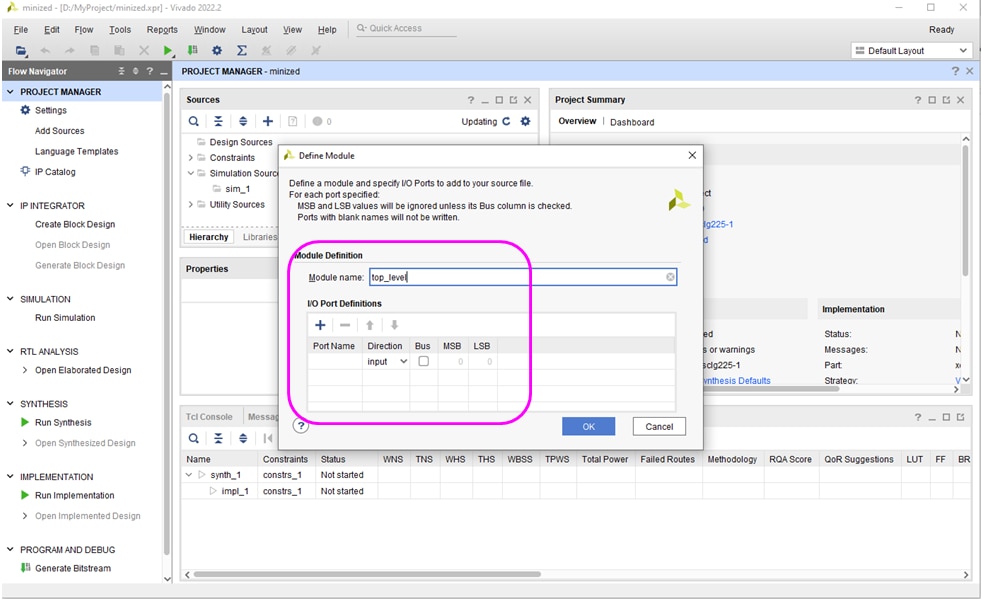
Next, I have selected the inputs and outputs to the “top_level” Verilog module:
I have created four pins: two inputs for the temperature set up and down buttons, which I have labeled PMOD1P1 and PMOD1P2, and two outputs for the cooler and heater elements, which I have labeled LED_Green and LED_Red (since in this step I am only connecting these outputs to LEDs).
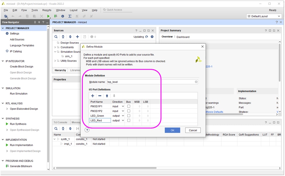
I have then clicked “OK” and next the Vivado tool has created a template frame for the Verilog module with these pins defined:
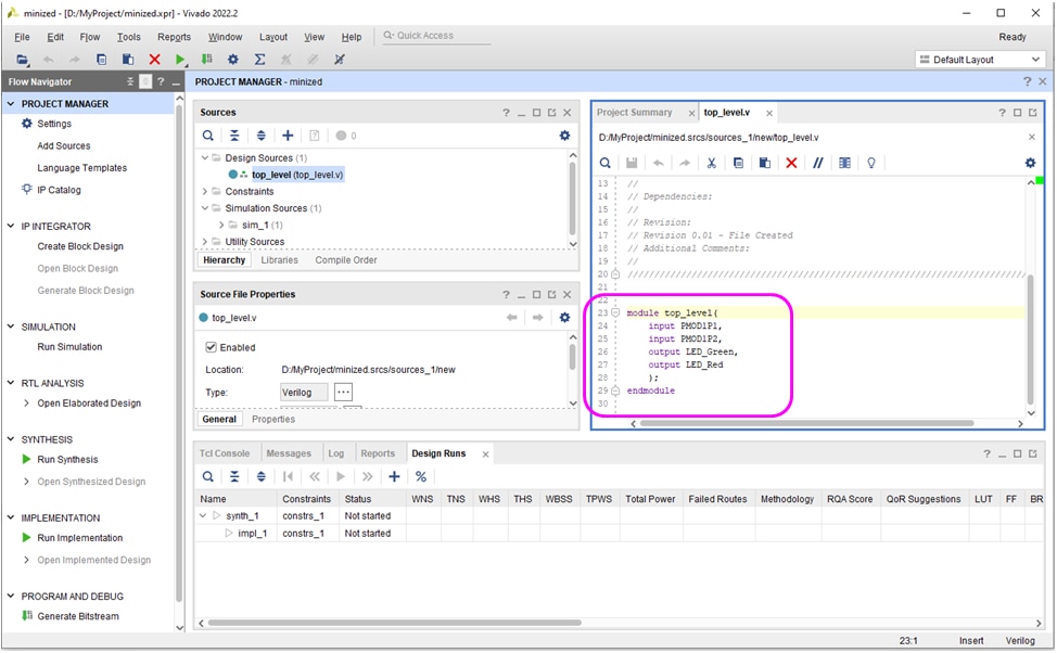
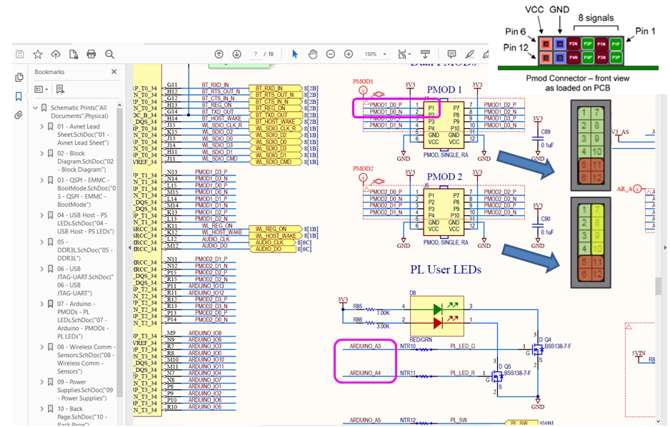
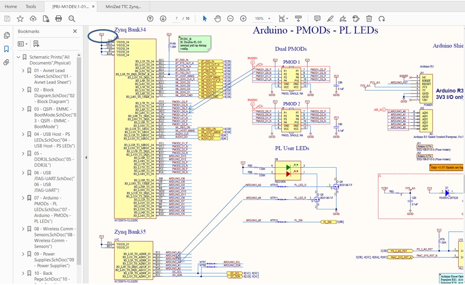
These pins correspond to the MiniZed board signals that are connected to the PMOD 1 connector and the Red and green LEDs:
In this “Step 1” of the project I only want to configure and test the GPIO interface, so to keep things simple I have chosen to connect the PMOD1P1 input to the green LED and PMOD1P2 to the red LED. This connection in Verilog is done using an assignment statement, like for example “assign LED_Green = PMOD1P1;”. Here is the updated Verilog code with these two assignment statements:
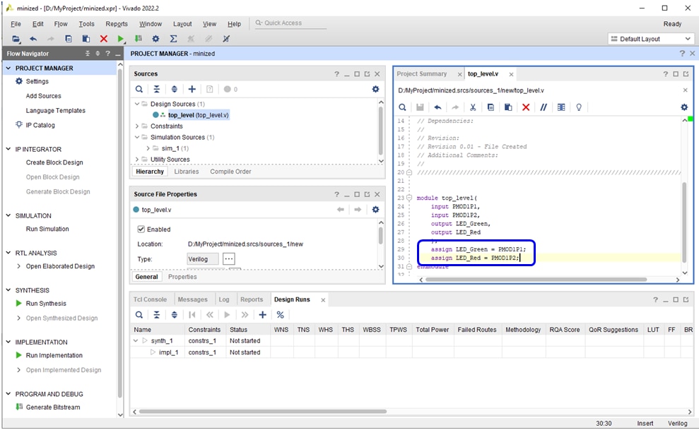
So I expect when I push the button connected to PMOD1P1 to apply 3.3V to that pin, which is interpreted as logic “1” or logic “True” by the Zynq PL logic circuits. This logic “1” value is then assigned to the LED_Green pin and sent through the GPIO interface to the MiniZed board where it lights up the Green LED. Similarly, when I push that other button I expect the Red LED to light up.
I have now a Verilog code that should be functional so next I will test it. But before that, I wanted to create a block design and a symbol for this module that I will place it in the block design.
So first I have clicked on “Create Block Design”:
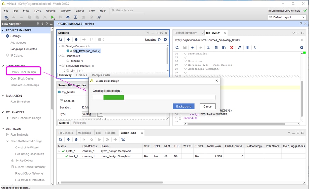
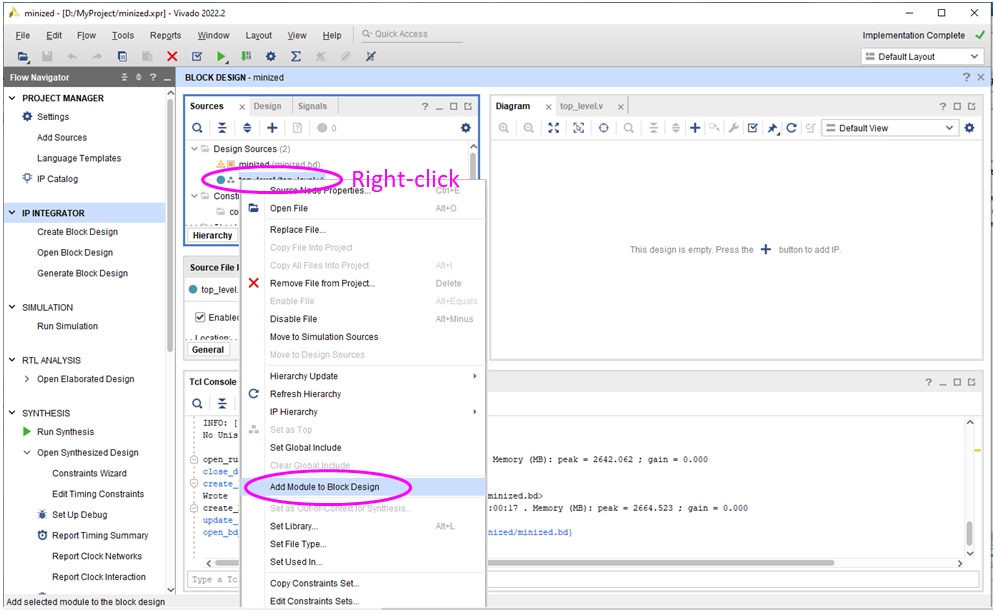
Next, I have right-clicked on the top_level verilog module and I have selected “Add Module to Block Design”:
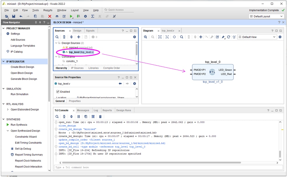
Vivado has created a symbol for the top_level module and placed it in the block design diagram:
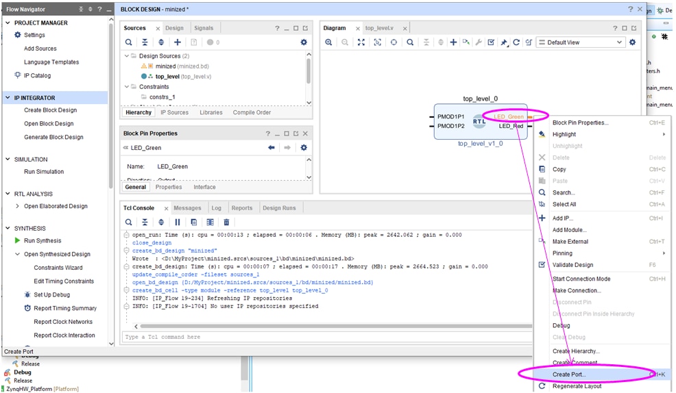
The Verilog module pins are shown on the symbol. Next, I have clicked on each pin and I have selected to “Create Port”:
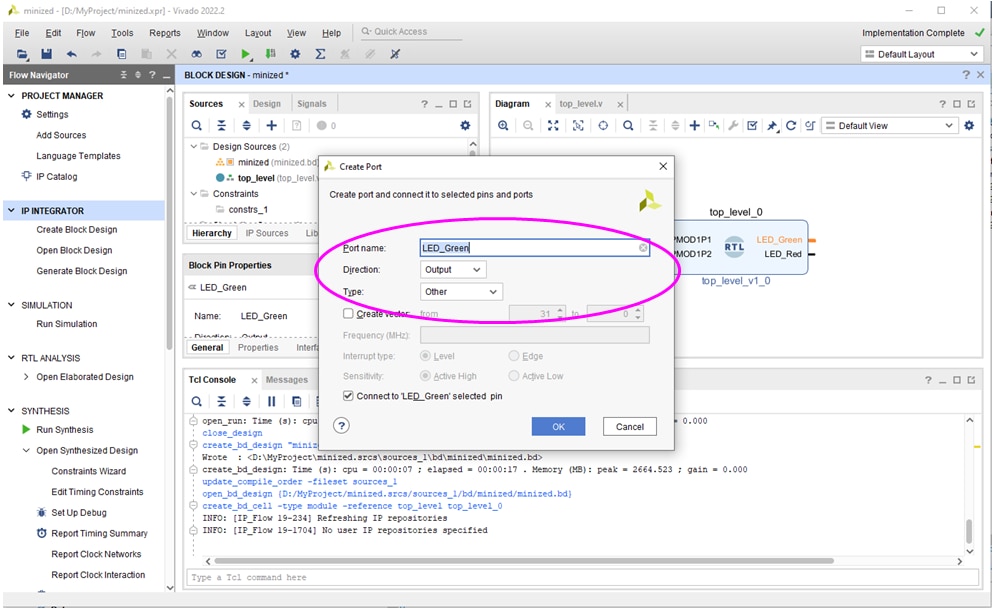
In the “Create Port” window I have defined the port name, direction, and type:
Then Vivado has added a pin symbol to the block design diagram:
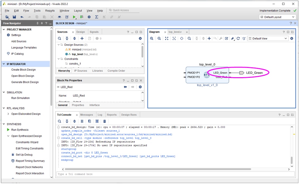
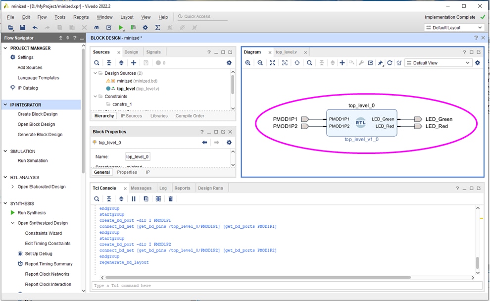
I have then repeated these steps and added ports for the rest of the pins:
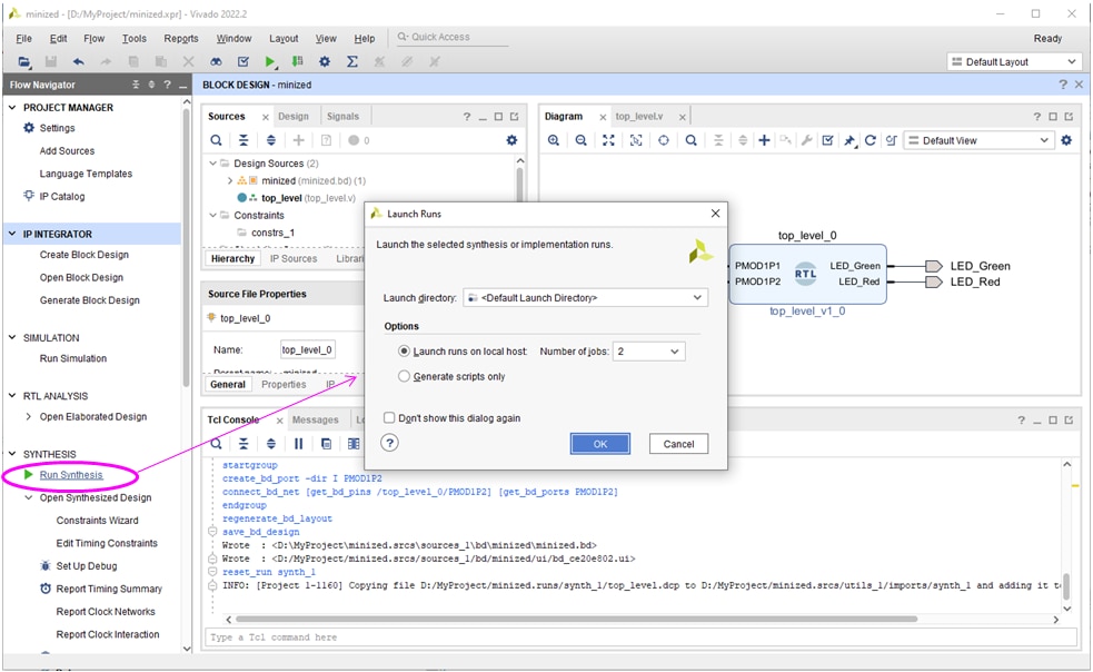
Next I synthesized the design:
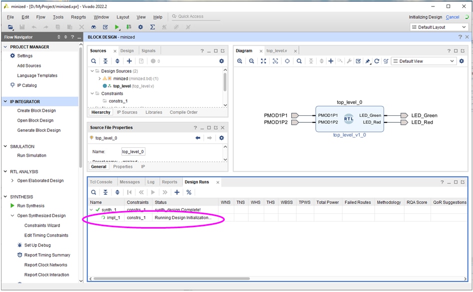
Then I run the implementation.
I need to remember that I have defined four pins that will be routed outside Zynq trough the GPIO interface, but I have not defined the location and the electric parameters for these pins. This is normally done though setting up the constraints prior to implementation. In my case I prefer to run the implementation first and then open the implemented design, which will assign some default values, and define the location and electrical parameters constraints by modifying what Vivado has put in there arbitrarily. So I click on “Open Implemented Design”:

Next I go to the I/O ports tab, which has the pin locations and I/O standard parameters:
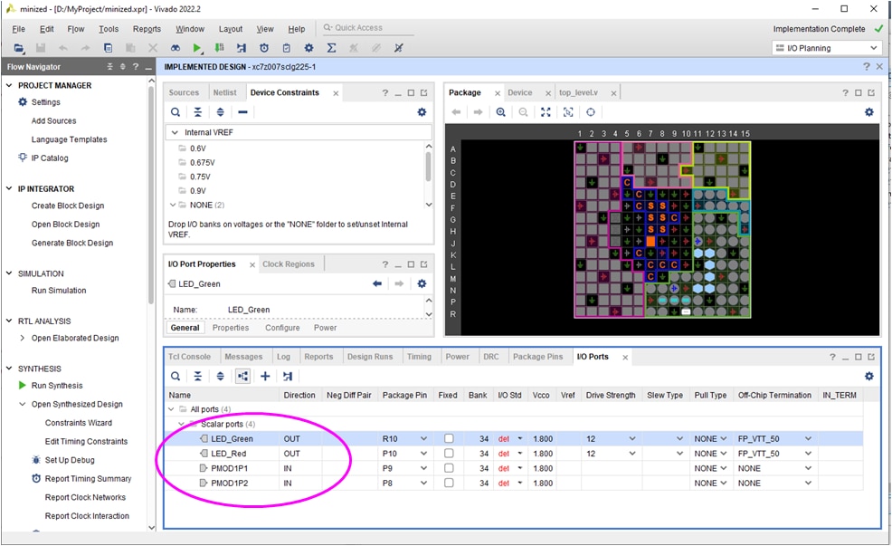
Now I had to look at the board schematic and pick the corresponding pins of the Zynq SoC that connect to the connector and LEDs that I am using:
So I edited the I/O ports from with this information:
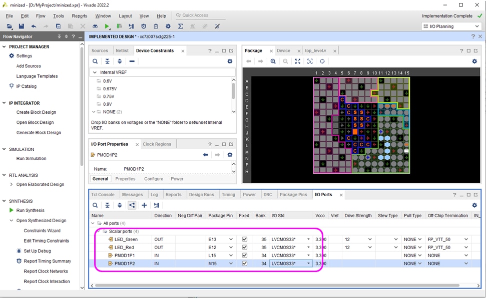
The I/O standard is now set to CMOS 3.3V, which corresponds to the I/O power supply on the corresponding banks 34 and 35. Next I have run again the synthesis and implementation with these updated I/O types and locations:
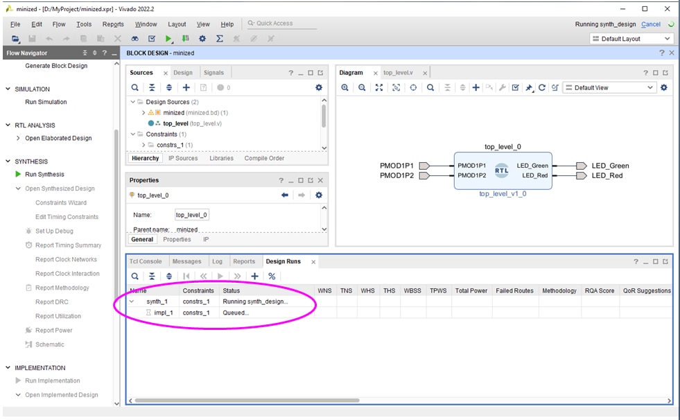
After the implementation run has completed I have generated the bitstream file:
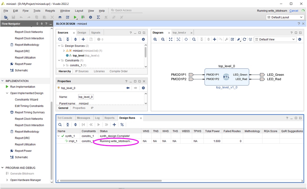
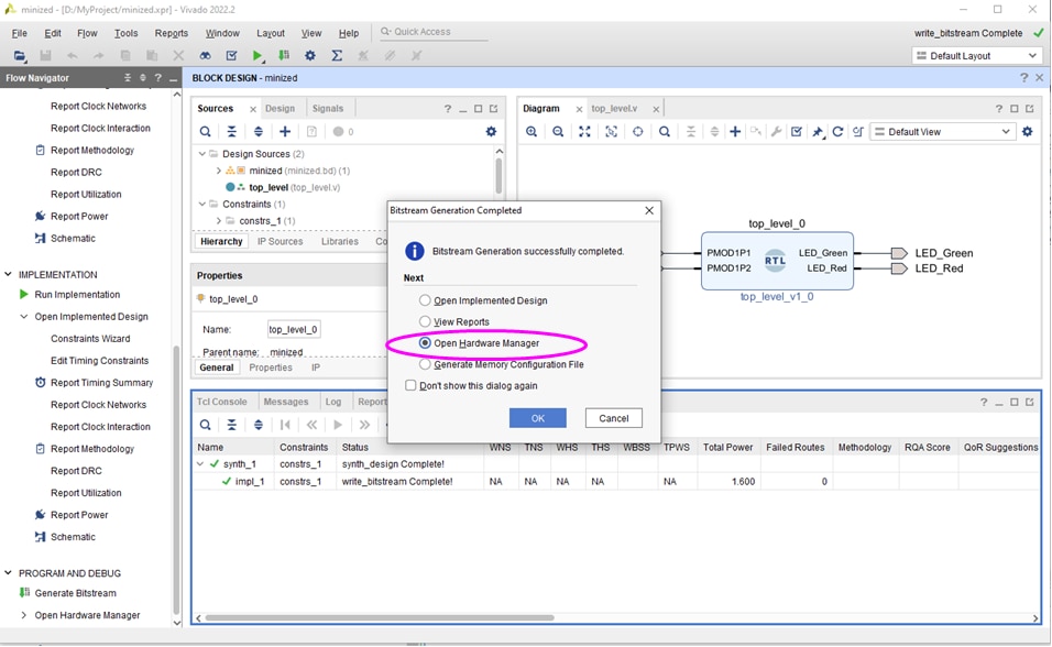
Next I have opened the hardware manager to program the Zynq SoC FPGA:
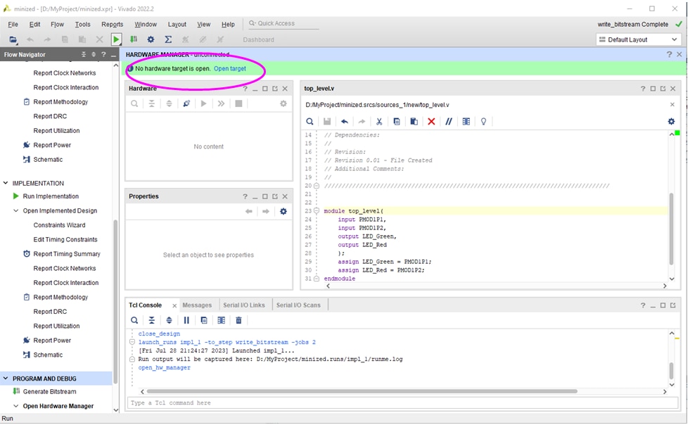
First step in the hardware manager was to open the target, which is the Zynq SoC FPGA on the MiniZed board:
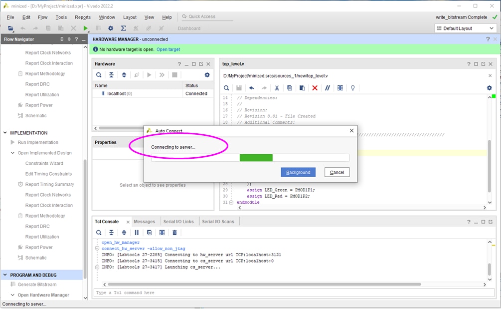
The hardware manager then connects to a local, which is probably part of the Vivado installed software:
The Zynq SoC is listed in the local host as xc7z007s_1 device:
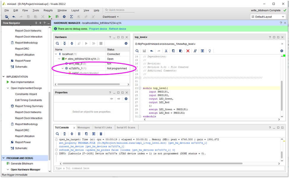
The Zynq is there but as the hardware manager shows it is not programmed. Next I right-clicked and selected program device:
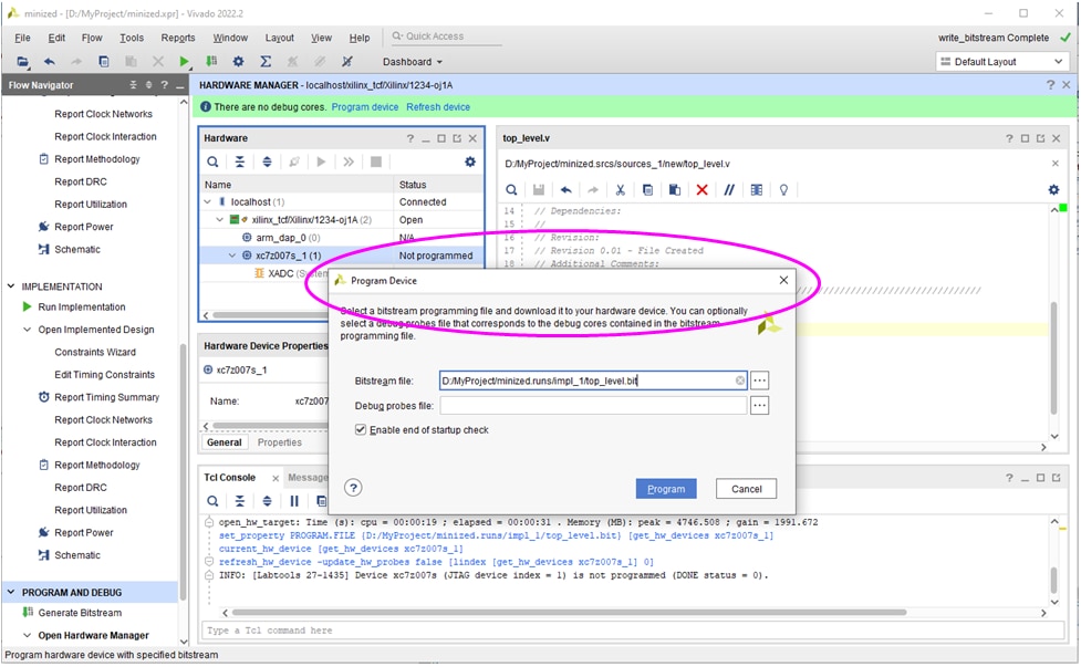
The path to the bitstream .bit file came automatically, so I only needed to press “Program”. The hardware manager then went through programming the device and when done it showed the Zynq SoC as “programmed”:
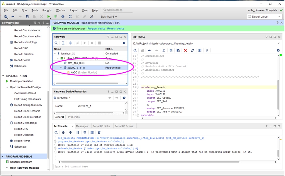
I was then ready to test the functionality of this simple experiment. Here is a video of me running the experiment:
The red and green LEDs were the ones built-in the MiniZed board. Next I wanted to add separate LEDs on the GPIO pins that will control the heater and cooler elements of this project. So I took a look at the MiniZed schematic and I picked different I/Os for the LEDS on PMOD2 connector pins 1 and 2 which are connected to pins P13 and P14 of the Zynq SoC as shown in the screenshot below:
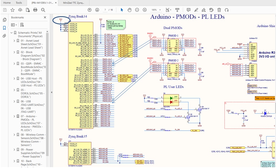
Then I opened the implemented design and I changed the location of the pins “LED_Green” and “LED_Red” to P13 and P14 pins of the Zynq SoC.
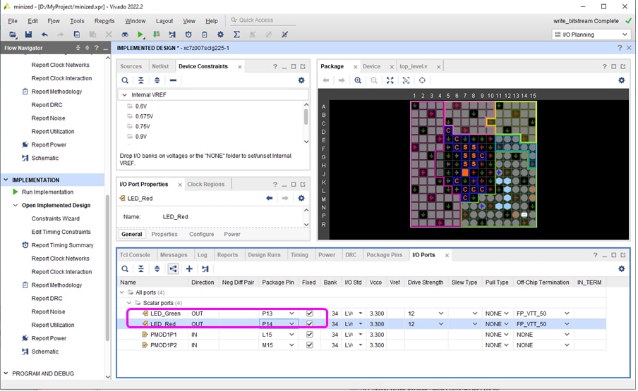
Next, I have run again the implementation and bitstream generation, and I have re-programmed the Zynq SoC. On the experiment setup in the lab, I have added two external LEDs connected to the PMOD2 pins 1 and 2 in series with series resistors to limit the current. Here is a picture of the test setup in the lab:
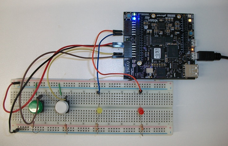
Next I ran again the lab experiment, as I am showing in the video below:
This concludes “Step 1” of this project. I then moved to “Step 2”.
Step 2
After I got the “confidence” that I can bring signals from “outside” to inside the Zynq SoC and I can drive signals from inside the Zynq SoC to the outside, in this step I will add flip-flops in the Zynq PL to “store” the logic values that I read from the two buttons (buttons for reading the user entry for adjusting the set temperature up or down). This step still uses only the PL of the Zynq SoC, so since in the MiniZed board there is no clock source connected directly to the PL I have decided generate the clock to the flip-flop externally from one push button.
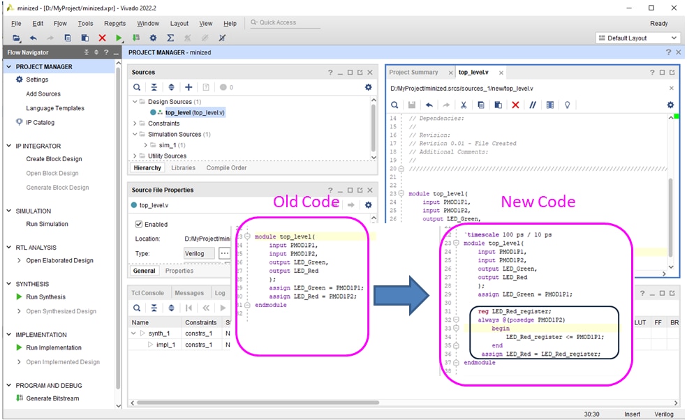
So first, I went back to the Verilog code in the “top_level” block and I added a register “reg LED_Red_register” which is different than an input and a wire since it has the capability to store a logic value (to memorize the value). This is what a flip-flop does; so it memorizes the input value on a transition of a clock signal and it keeps the value memorized until another transition of the clock happens (this is typical either a rising edge of the clock or a falling edge). This functionality is implemented with a “always @(posedge …) statement. The syntax and implementation is shown in the screenshot below:
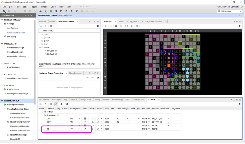
I also had to change the location of one of the input signals that I will use as clock, since the previous location did not allow a clock signal. Only a limited subset of Zynq input pins can be used as clock inputs:
Then I have synthesized, implemented, and generated the bitstream file for this new version of the project. The video below shows how I tested this “step 2” version of the design in the lab.
This concludes the second step. Next I have moved to “Step 3”.
Step 3
Now after I have validated that I can read data and store it in a flip-flop in the PL of the Zynq using an external “manually” generated clock, next I will add an internal clock signal to the flip-flops. The internal clock signal will be provided by the PS of the Zynq SoC. The PS receives an input clock signal from the MiniZed board, so I need to configure the PS to distribute a “copy” of that clock to the PL. Since this step uses the PS of the Zynq SoC, I will have to export the hardware from Vivado into Vitis and then use Vitis to compile the project and program the Zynq SoC.
First, I have added the Zynq processing system to the Vivado project. To do this I have clicked on the “+ sign at the top of the block diagram, and I have selected the “Zynq Processing System”.
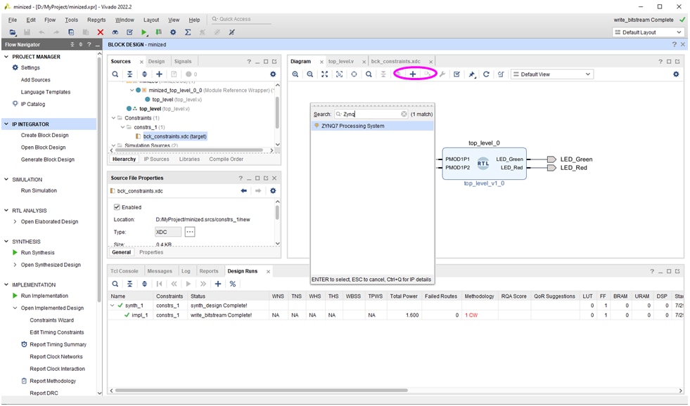
The Zynq processing system showed up in the block diagram next to the top_level symbol that we have placed before:
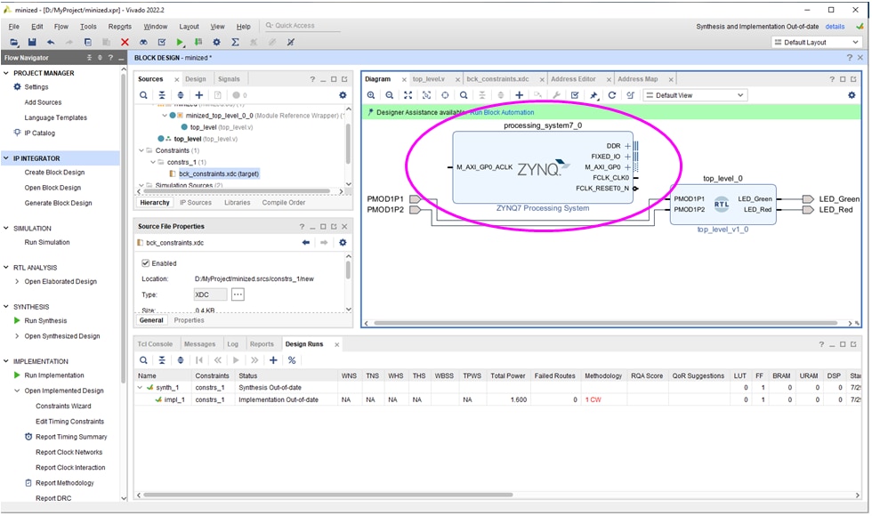
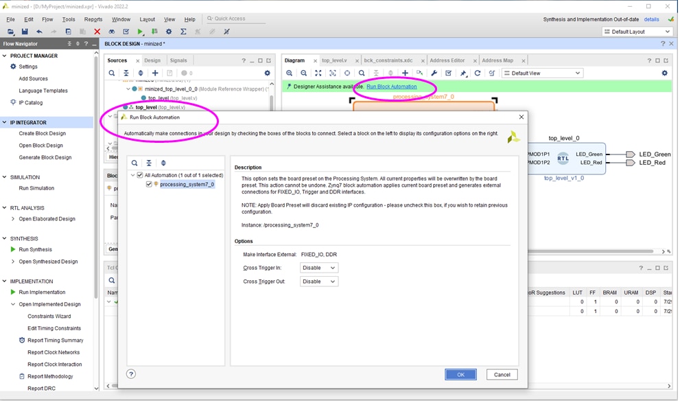
Next I have run the ”Block Automation”, which has added some of the connections from the Zynq processing system to the external pins:
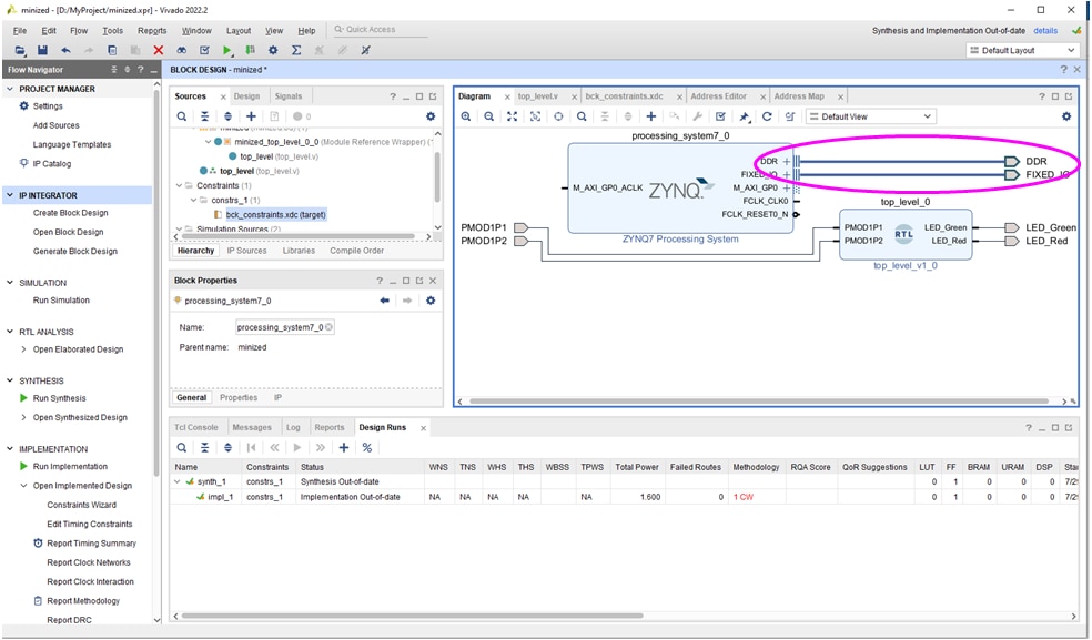
The DDR pins and the fixed IO pins are now connected to the Zynq processing system:
Initially, the Zynq processing system was “blank” not configured, so next I needed to configure it. To do this I have double-clicked on the symbol, which has opened the configuration window:
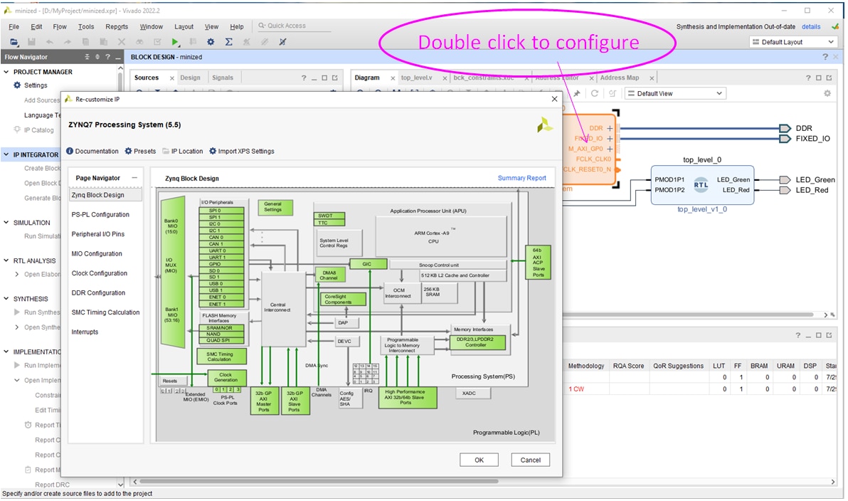
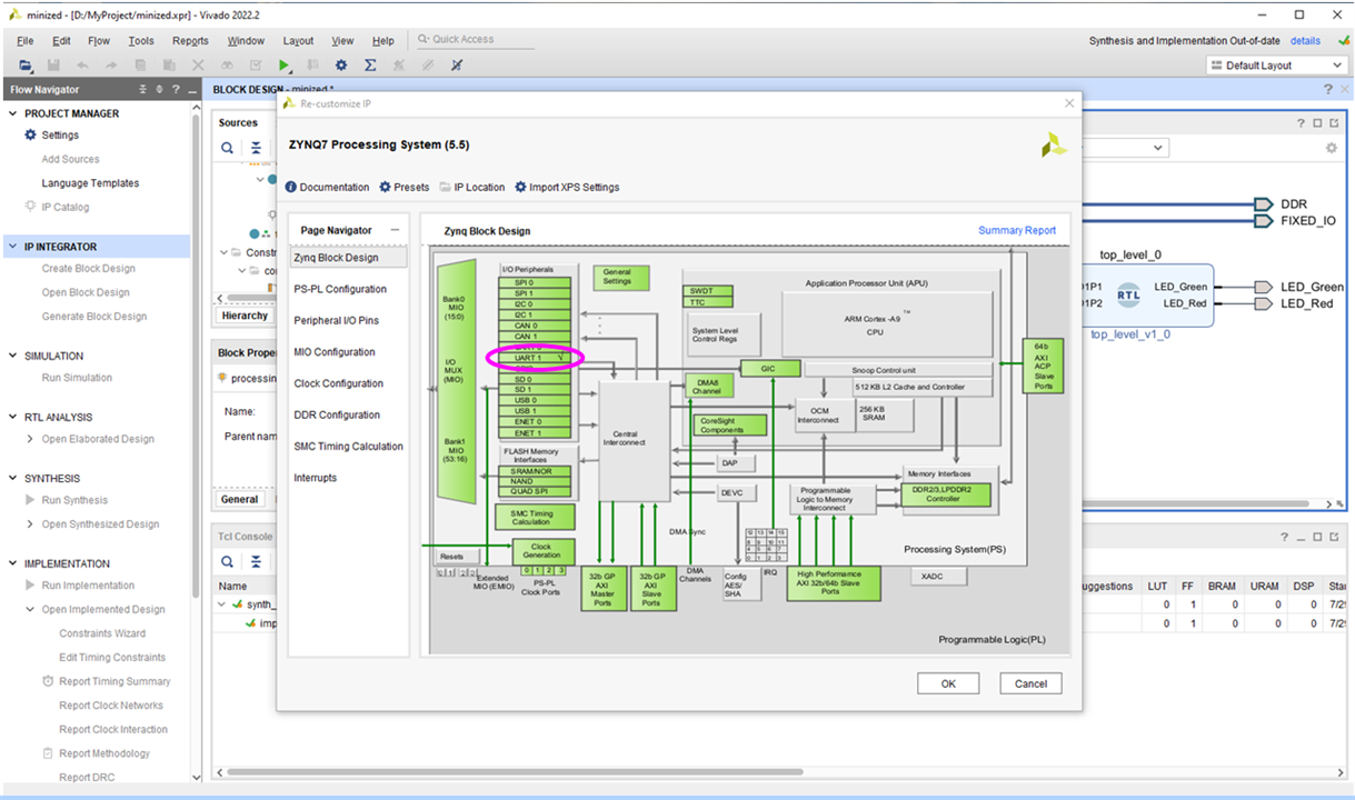
I need to enable the UART 1 interface that will communicate with the computer. I will use a COM serial monitor terminal on the computer to monitor the functionality of the code running in the processing system. Part of this communication, the code will write different messages and it will send measured values to the computer through this UART interface.
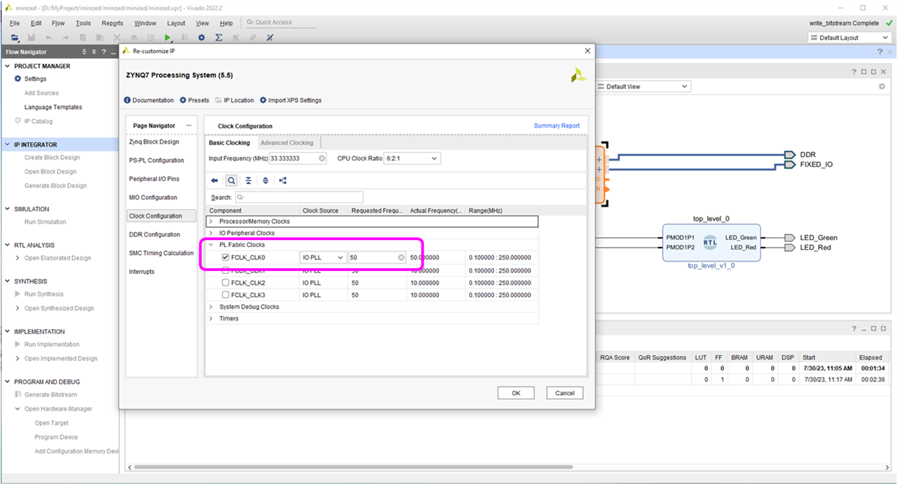
I also needed to enable the clock for the PL of the Zynq SoC, which will act as the clock for the flip-flops.
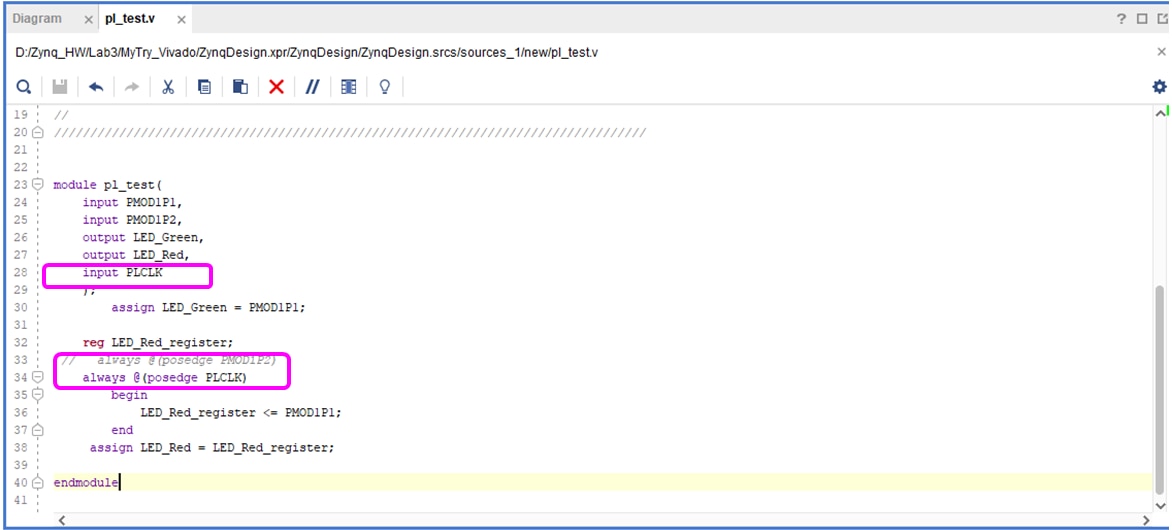
Next, I have added a clock input to the top_level verilog module. I named that clock input “PLCLK”. Then, in the Verilog code for the flip-flop I needed to replace the external button input that I used before as clock with the PLCLK clock. Here is a screenshot showing these changes:
Then, I updated the top_level symbol with the new clock input, and I connected the clock pin to the Zynq processing system:
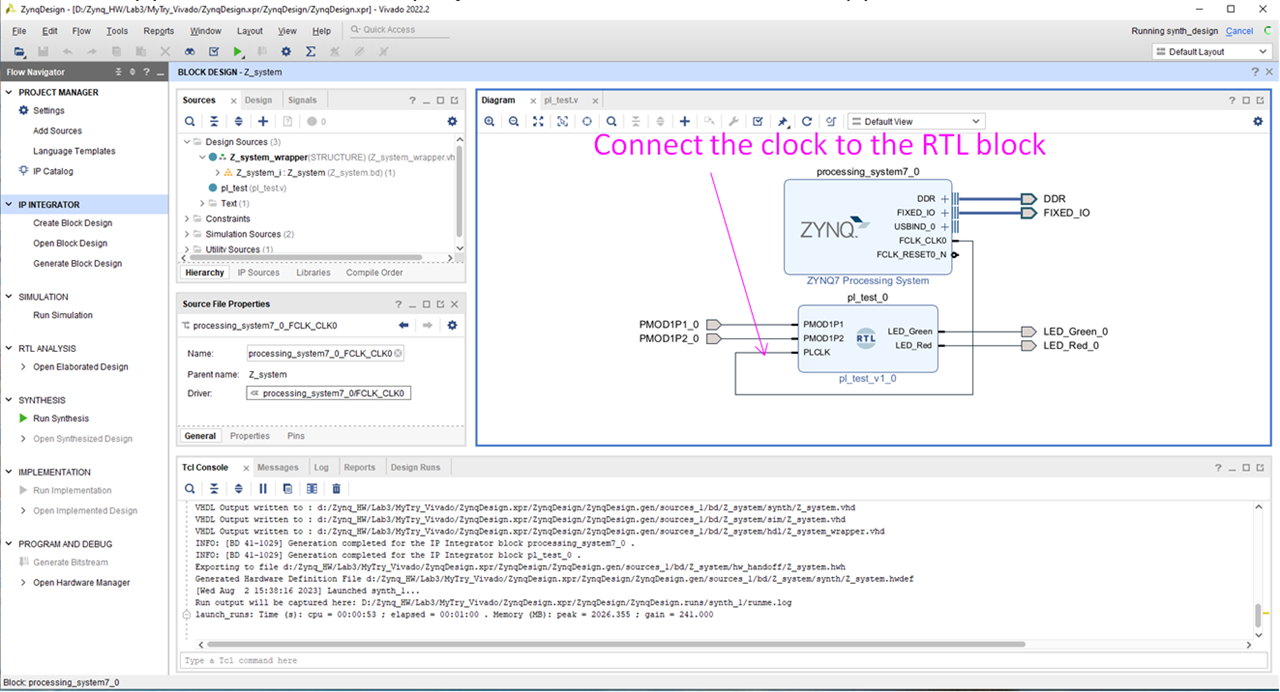
Then I run the synthesis, implementation, bitstream file generation. After the bitstream file has been generated, instead of programming the device I have clicked on “Export” and I exported the design to Vitis as a file called .xsa file. This .xsa file contains all the design information and the bitstream file (there is a checkbox that can be checked to include the bitstream file).
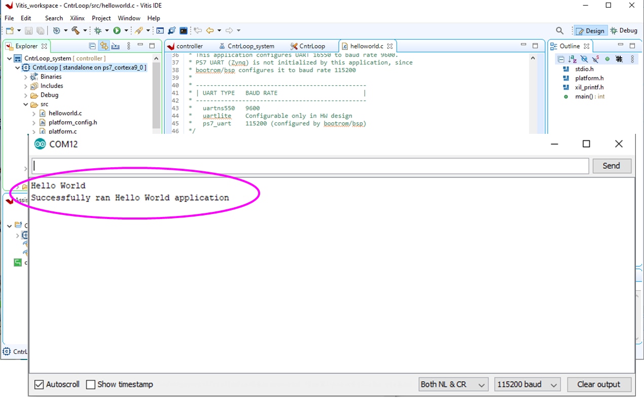
Next I moved to Vitis and I started by creating a platform project on the .xsa hardware file and then I have created an application project using the built-in “Hello World” template. Then I have built the project and have run the hello world application. No code changes were needed in Vitis for this experiment since I only use the PL clock of the PS to control the flip-flop in top_level RTL logic.
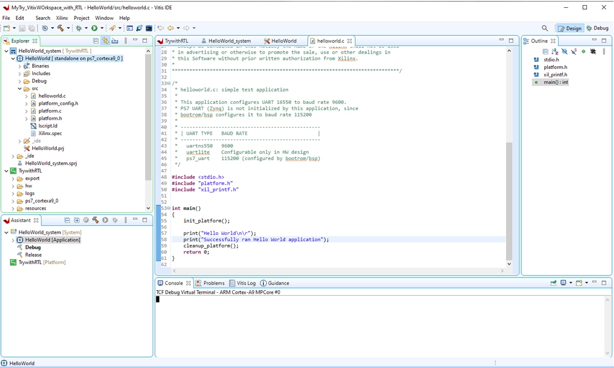
So I only needed to compile the project in Vitis and, when done, to right-click on the “Hello World” application and select “Run as” “Launch Hardware (Single Application Debug)”:
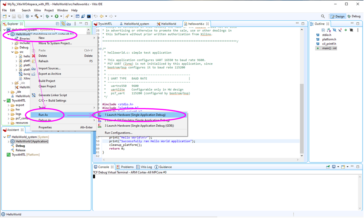
Then Vitis automatically programmed the Zynq SoC on the MiniZed board, and after that I was ready to check the functionality in a lab experiment. The lab experiment for this step is documented in the video below:
This concludes Step 3, and I am now ready to start Step 4.
Step 4
In Step 4 I will add the communication interface between the PL and PS. To do this I will have to create an AXI interface between Zynq PL ad PS and pass the temperature set buttons signals to PS through the AXI interface. I will also add two control signals for heater and cooler in the PS and route them to PL through the AXI interface.
To add the AXI interface block I had to go back to Vivado and to follow the same steps as for adding the processing system. So I clicked on the “+” sign at the top of the block diagram and I selected the AXI interface. After the AXI symbol got placed on the diagram I clicked on the “Run Block Automation” and then I manually connected the remaining inputs and outputs. Here is a screenshot of the completed diagram:
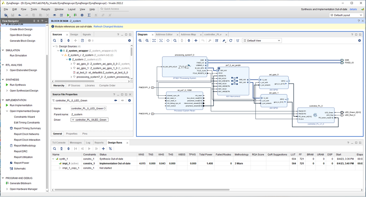
Notice that the design automation brings also a reset block “rst_ps7_0_100M” and connects it between the processing system and the AXI interface block.
Next, I have synthesized, implemented, and generated bitstream file in Vivado. When done, I exported the hardware to Vitis as .xsa file. Then I moved to Vitis, where I created a platform project around the .xsa file and then I created a simple “Hello World” application only to be able to compile and program so that I can run it on the Zynq SoC of the MiniZed board.
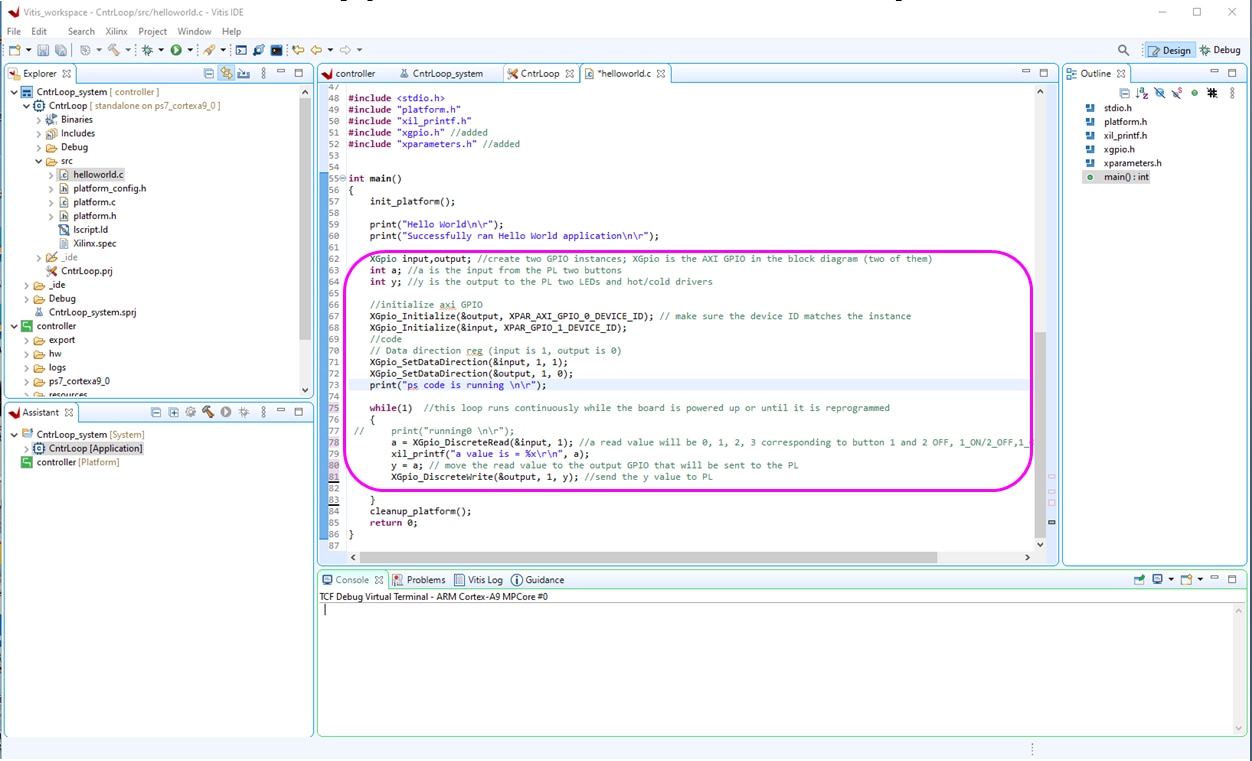
Then I edited the “Hello world” code to read the data from the external buttons through the PL and AXI and to send it back to the LEDs also through the AXI and then PL. This is to validate that my system can read data in PL and can pass that data to the PS through the AXI interface, and the other way send data from PS to PL through the AXI interface and then from PL to the outside to the external LEDs. Here is the code with annotated descriptions:
Next, I compiled the project in Vitis and I have run the application same as I did before with the Hello World test: “Launch Hardware (Single Application Debug)”. The lab testing is captured in the video below:
This concludes Step 4, and I am ready now to start Step 5, which builds the temperature control system.
Step 5
Now, after I have implemented and validated the project infrastructure in both PL and PS of the Zynq SoC, I will develop the temperature control software code that will execute in the Zynq PS microcontroller. Outside the MiniZed board I will add the HTU21D temperature sensor, a resistor as heating element, and a mini fan as cooling element. The schematic of this temperature control system is shown in the figure below:
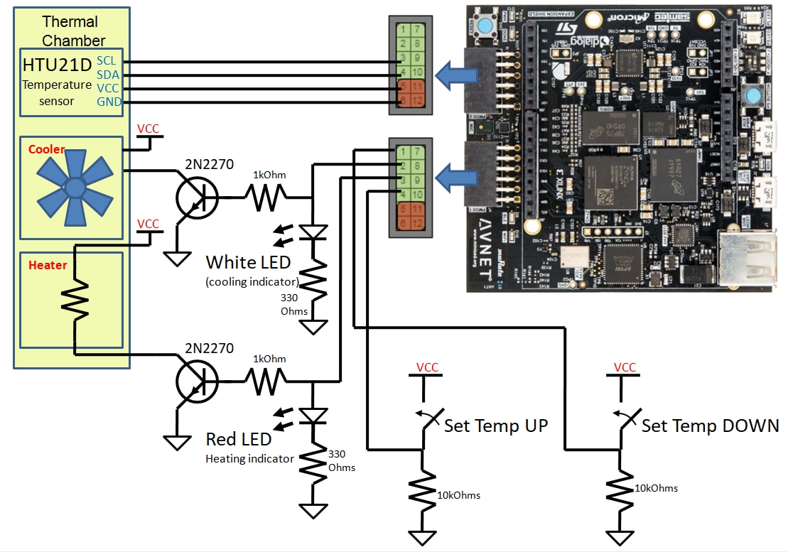
The HTU21D temperature sensor is connected to the Zynq SoC through an I2C interface having the SDA signal on 4 of the PMOD2 connector and the SCL signal on pin 3 of the PMOD2 connector. The drive strength of the Zynq SoC GPIOs was not enough for driving the heater and the cooling fan, so I added two 2N2270 power BJT transistors that can drive 1A currents. I have also added two LEDs, one of them color white lights up when the cooling fan turns on, and the other one color red lights up when the heater is turned on. The thermal sensor, heater, and cooler are mounted in a structure that I call “thermal chamber”. The temperature sensor measures the temperature of the thermal chamber, the heater heats up the thermal chamber, and the cooling fan cools down the thermal chamber. The set temperature adjust buttons are connected to pins 1 and 4 of the PMOD1 connector. When either button is pressed, the corresponding input is pulled to Vcc=3.3V. When a button is not pressed, the corresponding input is “weakly” pulled down to ground through a high value 10k resistor.
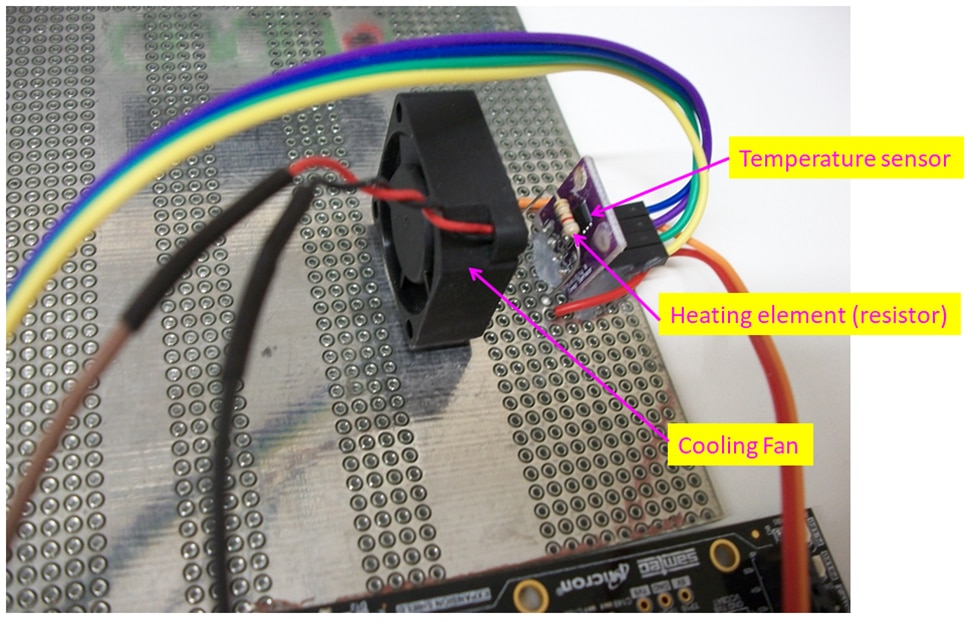
The lab fixture implementation is shown in the picture below:
The “thermal chamber” structure contains the temperature sensor, the heating resistor, and the cooling fan, as shown in the image below:
The HTU21D temperature sensor communicates with the Zynq SoC through an I2C interface, so I had to configure that interface. TO do this, I went back to Vivado and I opened the block design. At the top I clicked on the “+” sign same as I did before when I added the processing system and the AXI interface. This time I selected a block named “AXI IIC” and then Vivado has placed it on the block design. Next, I double-clicked on this new block to open the configuration window:
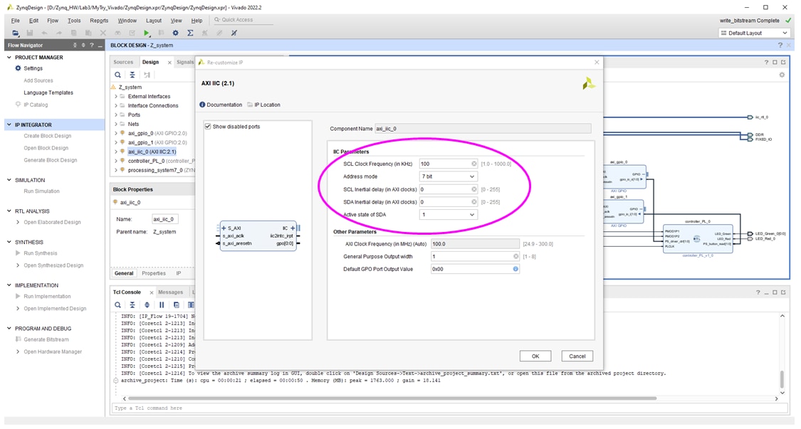
In this window I configured the clock frequency and for the rest of parameters I used the default values. Then, I closed this window and I clicked on “Run Design Automation”, which has routed the I2C AXI block into the existing schematic.
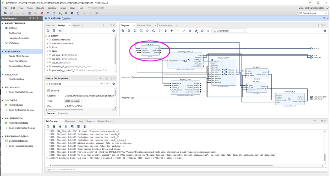
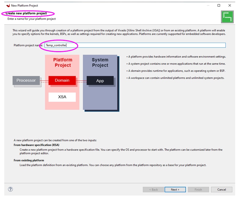
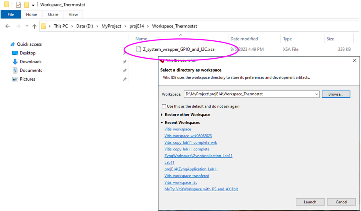
Next, I built the project, synthesized, implemented, and generated the bitstream file. When done I exported the .xsa file for Vitis. Then I moved to Vitis where I created a platform project that uses the newly generated .xsa hardware file:
,and I select the .xsa file:
Then, I created a platform project named “Temp_controller”:
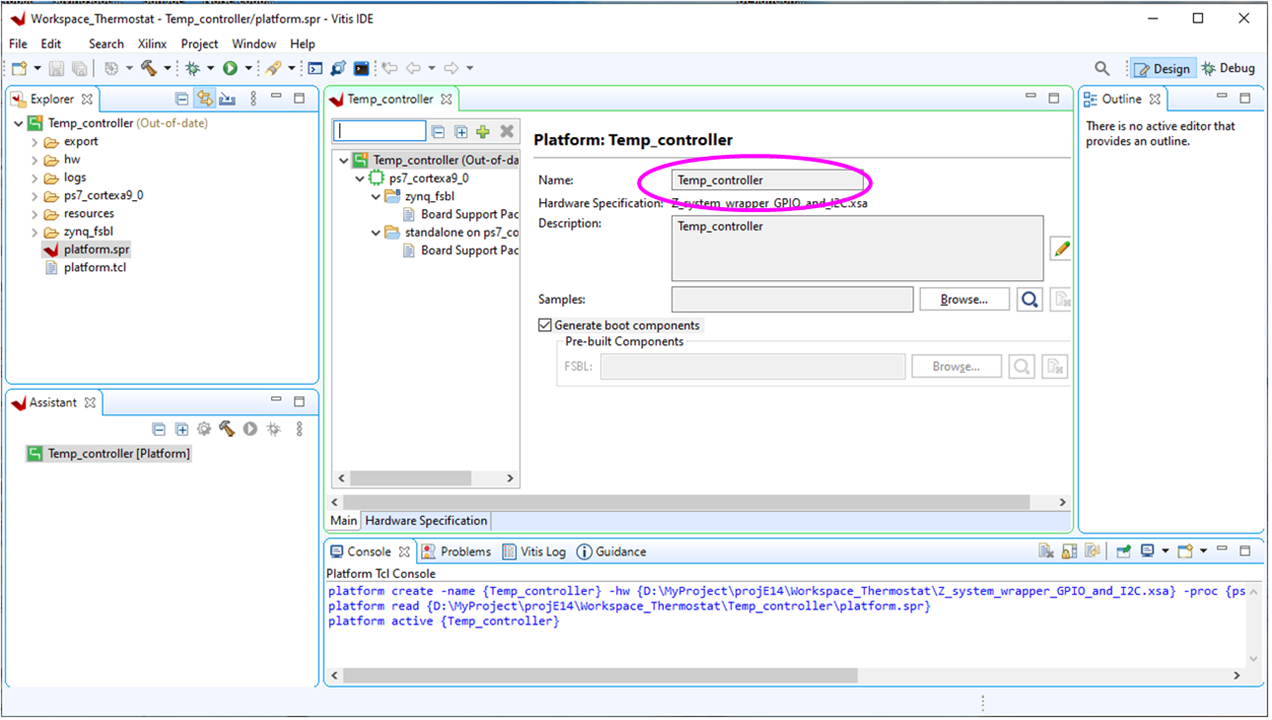
Next, inside the “Temp_controller” platform project I created an application project named “CntrLoop”:
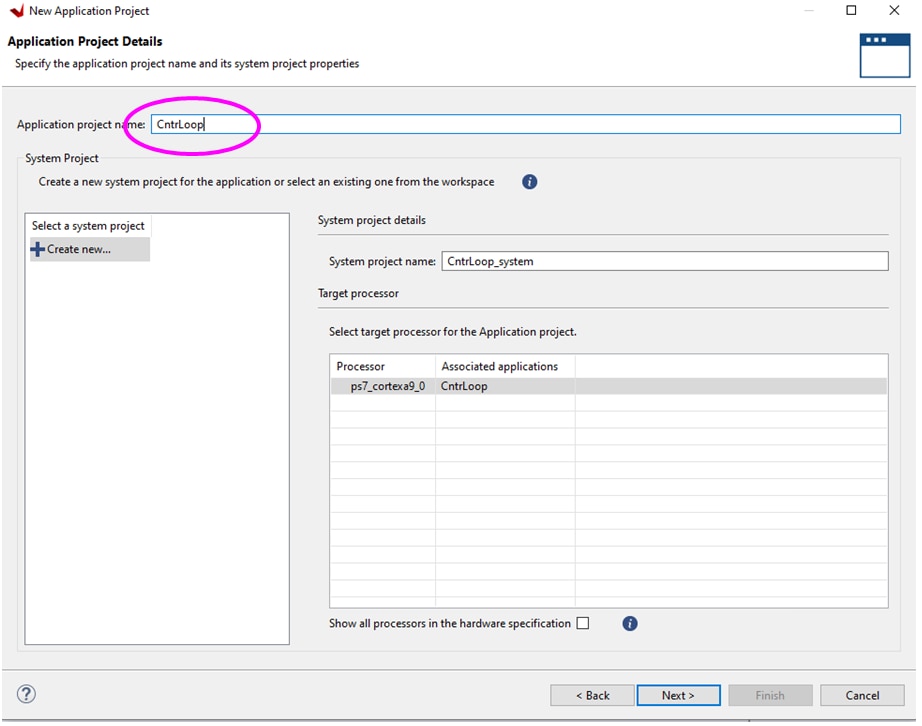
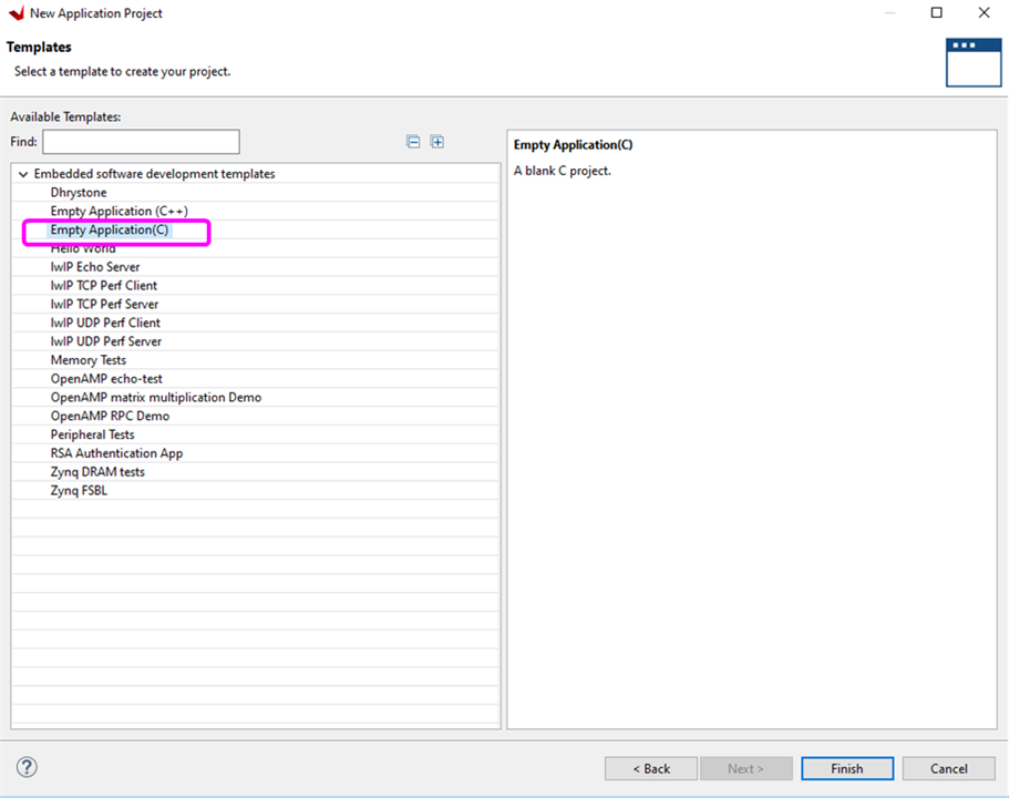
For this application project I have chosen as template “Empty Application” in C language:
Next I imported the sources from the project version in “Step 4”:
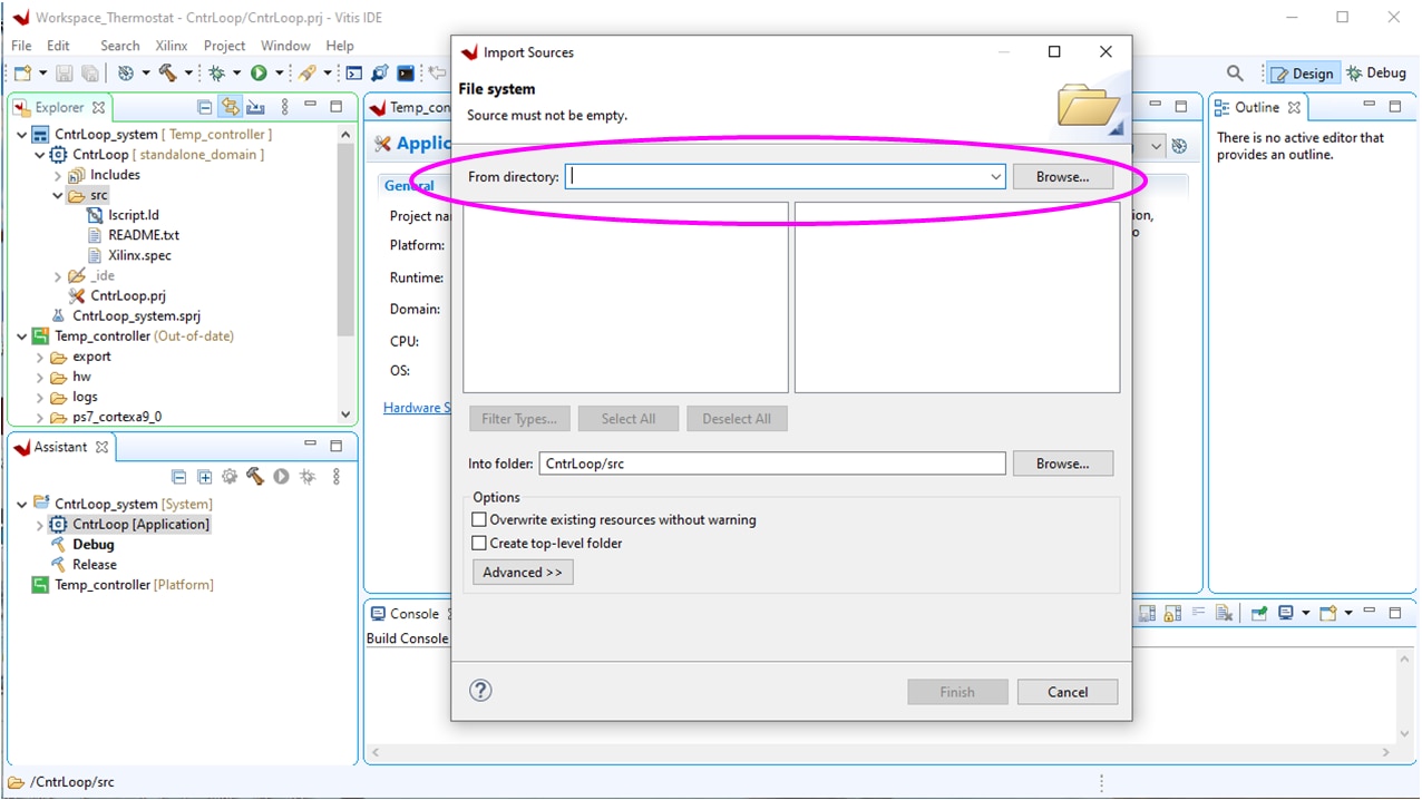
The imported sources were then shown in the “CntrLoop” application project:
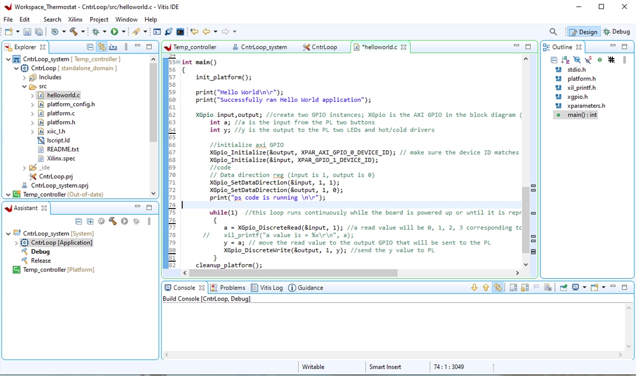
This software code was the starting point for developing the code for step 5 of this project. This starting point code has been validated experimentally in “Step 4”, which gave me the confidence that the Zynq PL is configured correctly and the interface between PL and PS is functional.
Next step, I added the initialization for the HTU21D temperature sensor, for which I have got inspiration from the training course Lab 11 of the software section. So I needed to add the htu21d.h library and to initialize the AXI block for the I2C interface. I also needed to initialize a starting value for the temperature set, which I set to 26C.
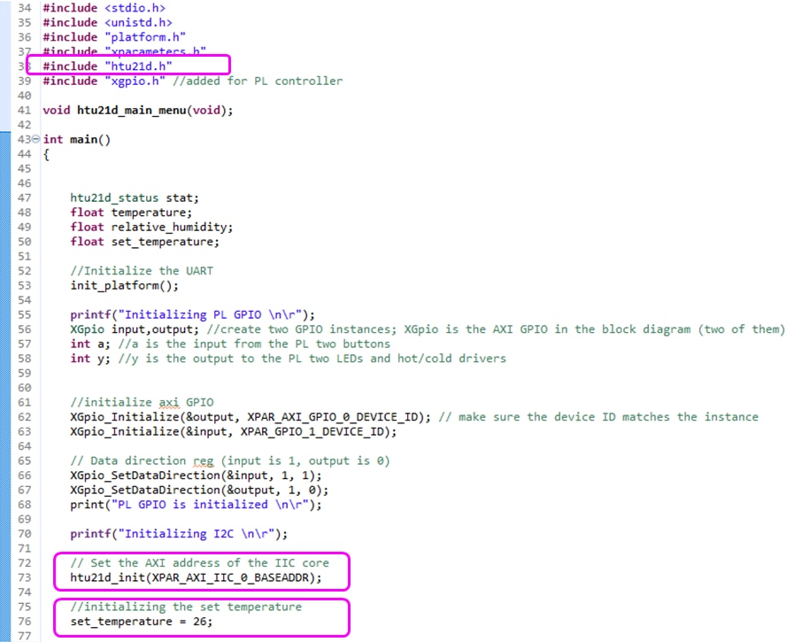
All the initializations are done now, so I can move to developing the code for the continuous running loop. Here I needed to go back to the flowchart and write a code that follows the sequence of functions in that flowchart. However, after the experience I gained during these steps, I realized that I should re-arrange the flowchart. The modified version has the same steps as the original flowchart, but arranged in a more convenient sequence. So the functionality stays the same. Here is the initial and the modified flowchart:
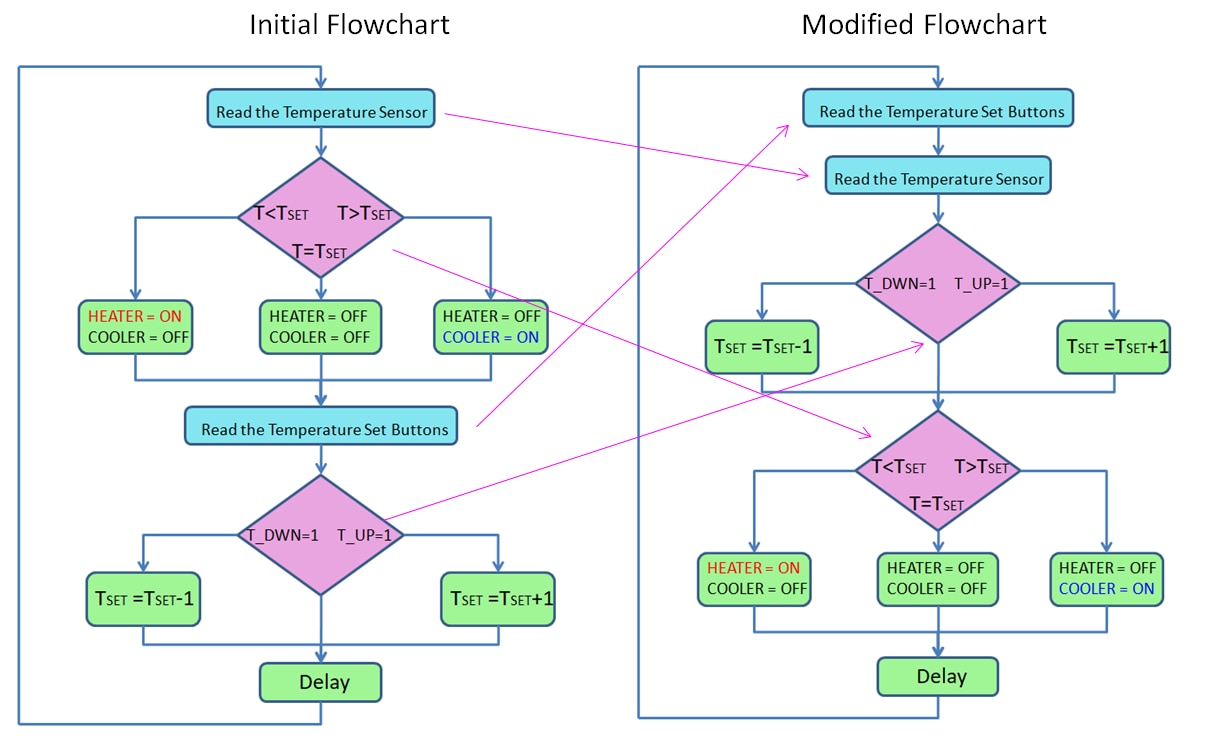
Following the modified flowchart, I have then developed the control loop code as a continuous “While” loop. Here is the code that I have written with annotated correspondence to the flow chart functions:
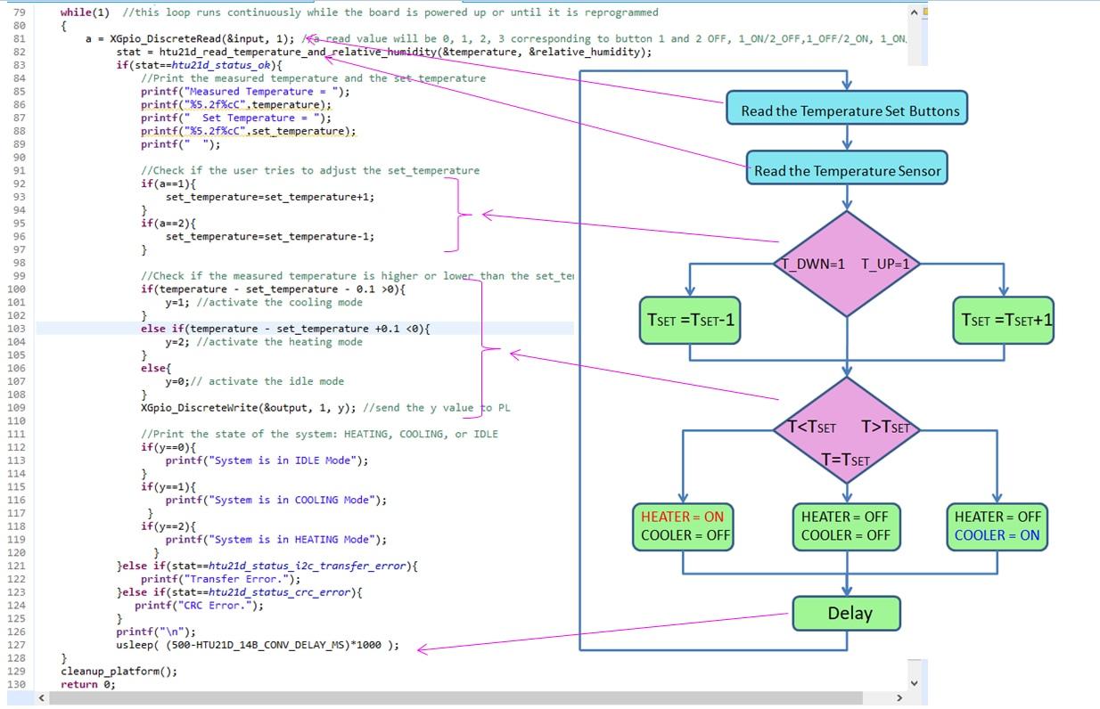
I have also added a few “printf” statements to send data to a serial monitor window on the computer. This way I can follow the functionality of the control loop, though the connection to the computer and the serial monitor is not needed for the functionality of this temperature control system. The system will work the same if I don’t connect it to the computer.
The temperature control system is now ready to be tested. To test it, I used Vitis run function for this application project to program the Zynq SoC and run various experiments to check the functionality. The MiniZed board was connected to a computer where I started a serial monitor window from the Arduino IDE tool. In the experiments, I used the serial monitor window to follow the functionality of the temperature control system as it went through the experimental stimuli and user commands.
The next section of this blog will describe some of the experiments that I ran in the lab.
Lab Experiment 1
In this first experiment I have set the temperature comparator window to zero, and I have just watched how the temperature control system maintains the “thermal chamber” temperature at the programmed value of T_set = 29C by turning ON and OFF as needed the heating element and the cooling fan. Here is a video that shows this experiment:
We see in this video how the temperature control system alternates in turning ON and OFF the heating element and the cooling fan to keep the temperature constant. This control process has been recorded on the serial monitor window, and I am showing a partial screenshot below:
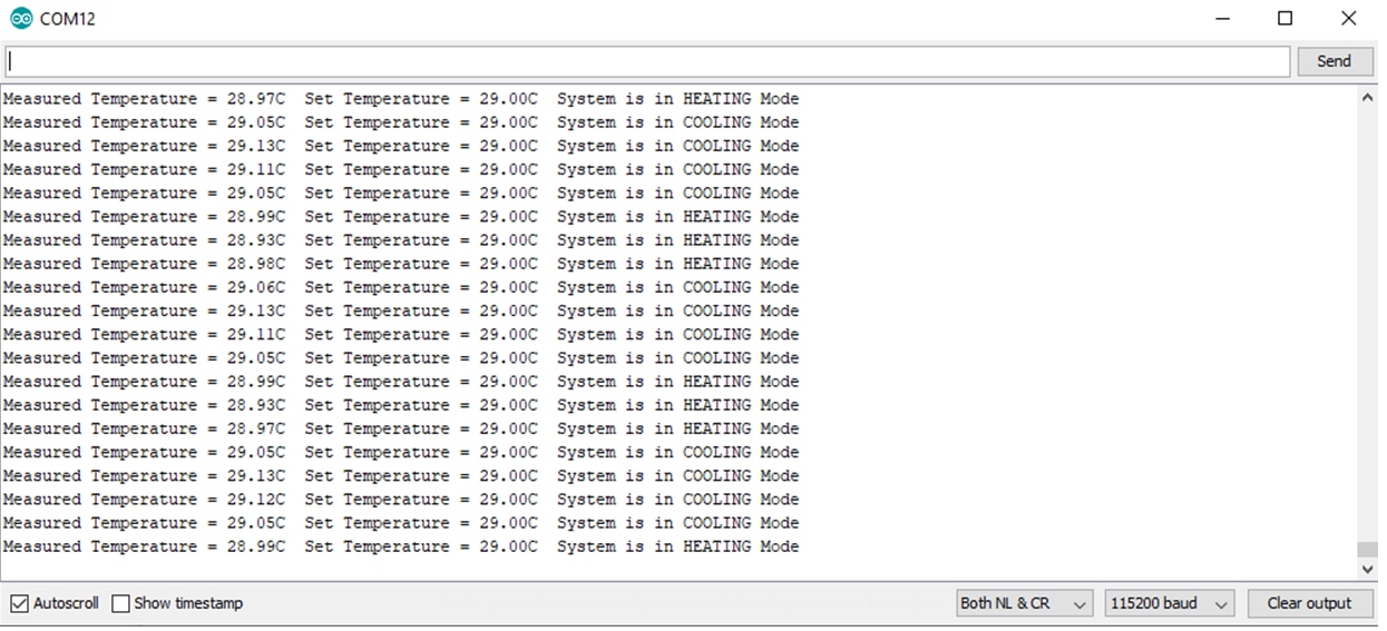
In this screenshot we see that the measured temperature “bounces” around 29C, which is the value of the “Set Temperature” programmed by the user and shown in the second column of values. The third column is informative only, and it displays the state of the temperature control system. In this case the temperature control system switches between cooling and heating.
The display on the serial monitor window is generated by this part of the code:
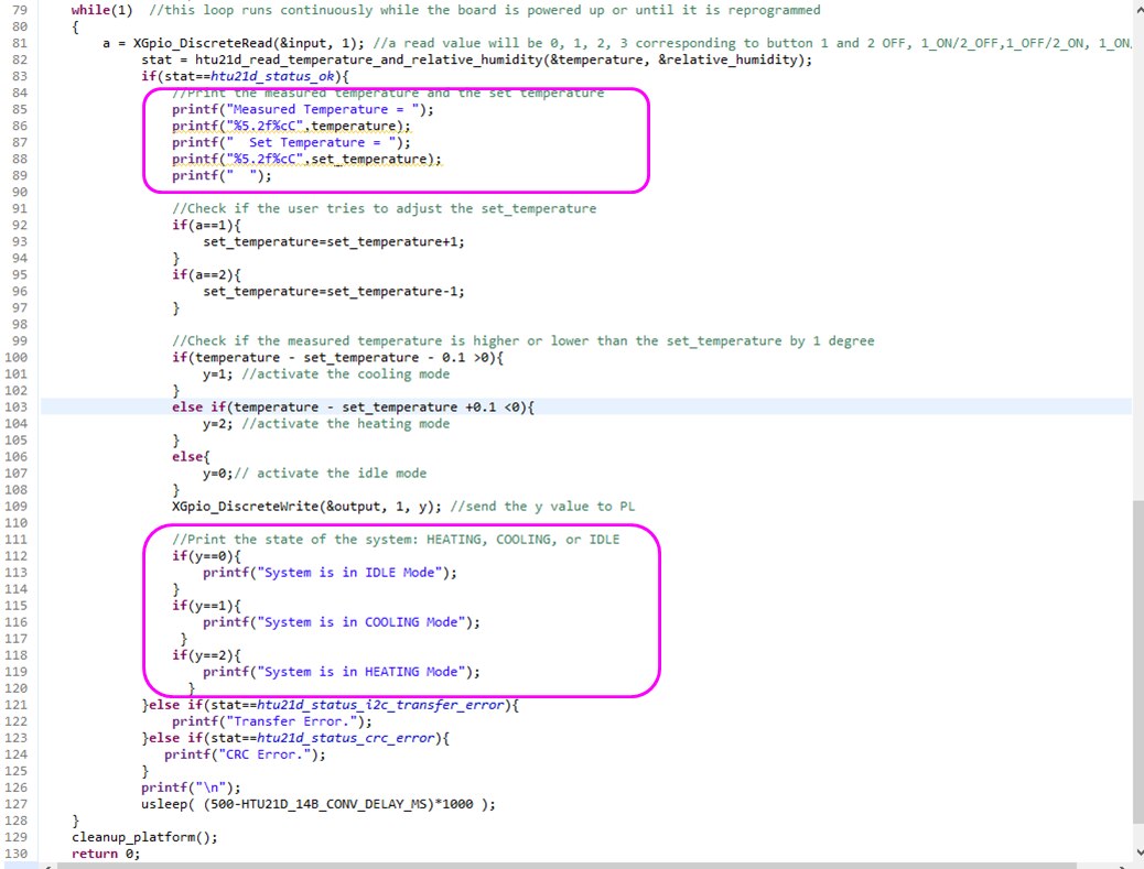
There is also a “IDLE” mode, but the system does not go in “IDLE” because the comparator window is set to zero. In the following experiments I have defined a non-zero comparator window and the system will sometimes be in “IDLE” mode.
Lab Experiment 2
The temperature comparator window of 0C, used in the first experiment, made the temperature control system change the operation mode continuously bouncing between cooling and heating. This functionality mode is not recommended since it puts stress on the components of the system. So I have setup a window in the temperature comparator of +/- 0.1C. This means that if the measured temperature is within the set temperature +/- 0.1C the system stays in “idle” mode and it keeps OFF both the heating element and the cooling fan. This modification required me to re-build the application and re-program the Zynq SoC. In this experiment I have setup the programmed temperature at 28C, which was a little lower than the initial “thermal chamber” temperature. So I expected the temperature control system to try to maintain the temperature at 28C +/-0.1C, thus between 27.9C and 28.1C. When the measured temperature is within this window the system should keep the heating element and the cooling element OFF. Here is a video that shows this second lab experiment:
We can see in the video how the thermal control system turns ON and OFF the cooling fan trying to keep the measured temperature in the 28C +/-0.1C window. When the measured temperature is within this window the system goes in “idle” mode, as recorded also on the serial monitor:
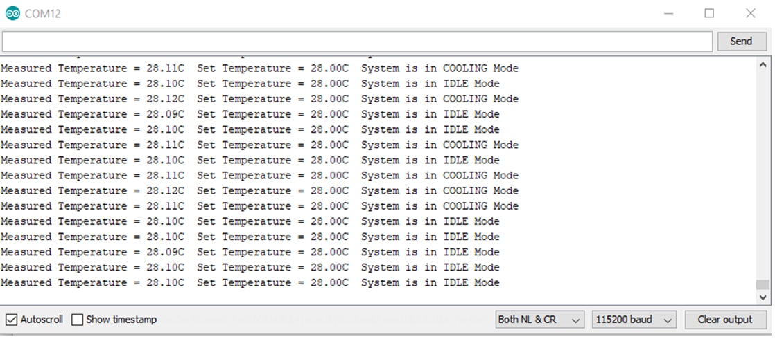
The temperature is controlled at the higher limit of the set temperature window, so only the cooler needs to turn ON and stay on until the temperature decreases below this higher limit. Then the cooler stops and the temperature rises gradually. The system stays in “IDLE” mode for some time before the temperature increases outside of the comparator window.
Lab Experiment 3
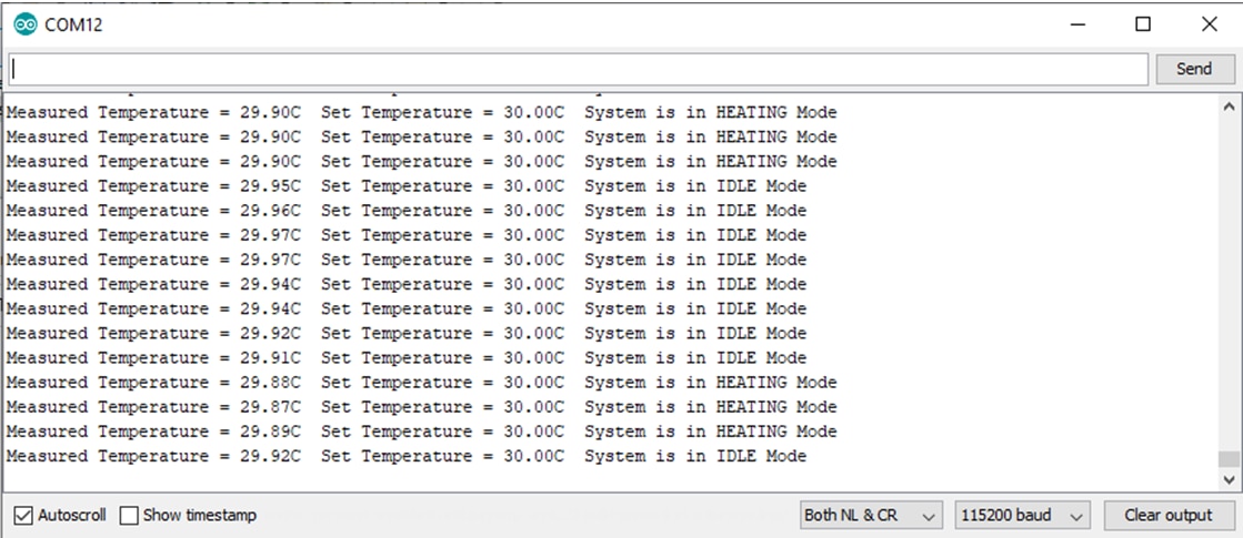
In this experiment I have setup the programmed temperature at 30C, which was a little higher than the initial “thermal chamber” temperature. So I expected the temperature control system to try to maintain the temperature at 30C +/-0.1C, so between 29.9C and 30.1C. When the measured temperature is within this window the system should keep the heating element and the cooling element OFF. Here is a video that shows this second lab experiment:
We can see in the video how the thermal control system turns ON and OFF the heating resistor trying to keep the measured temperature in the 30C +/-0.1C window. When the measured temperature is within this window the system goes in “IDLE” mode, as recorded also on the serial monitor:
Lab Experiment 4
In this experiment I wait until the thermal control system brings the temperature within the set window when the system enters an “equilibrium” state, and then I change the set temperature down by 1 degree by pressing one of the temperature adjust buttons. I then watch how the system turns the cooling fan ON and brings the temperature down at the newly programmed value. Here is a video showing this experiment:
Notice in the video how immediately after I pressed the temperature adjust button the cooling fan has turned ON (indicated by the white LED and the fan rotating). After the temperature is lowered within the programmed window the cooling fan stops and the system goes in idle mode (both cooling fan and heating resistor are off). Then after a while, the heating resistor is momentarily turned ON because the temperature has decreased too much and got below the lower limit of the programmed window.
Lab Experiment 5
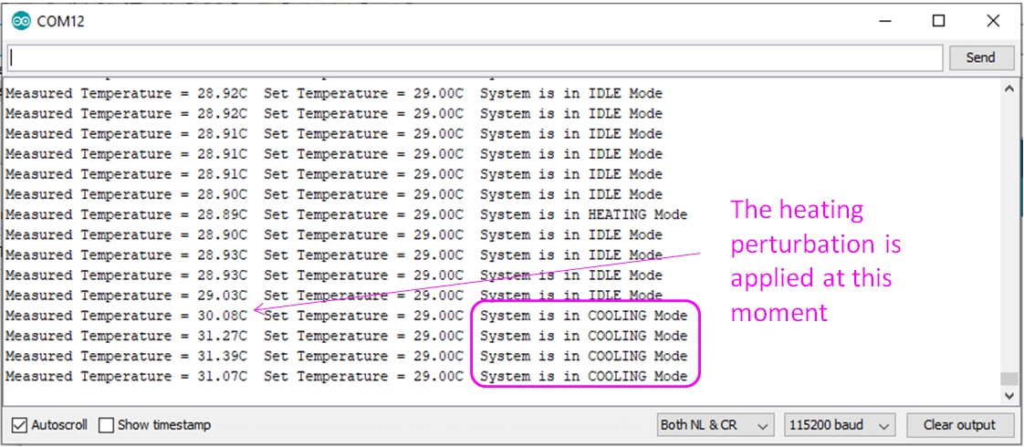
In this experiment I wait until the temperature control system brings the temperature within the set window and enters an “equilibrium” state. Then I apply a thermal perturbation in the form of a hot air hair dryer, which momentarily heats up the “thermal chamber”. Then after I remove the perturbation I watch how the system brings back the temperature towards the programmed value by turning ON the cooling fan. Here is a video showing this experiment:
The serial monitor sows the moment the hair dryer started to heat by the measured temperature jumping from 29C to 31C, and in that moment the cooling fan is activated:
These experiments have tested the main functions of the temperature control system that I have built.
Conclusion
My goal for this project was to start “from scratch” and design a control system implemented in the Zynq SoC on the MiniZed board. Besides being an engineer I am also a teacher, so in this project I have focused on following an “academic” path by starting from a concept block diagram, then developing a functionality flowchart, and then developing the system in a structured logical way layer by layer by understanding and validating each layer before moving to the next one.
This blog has followed me developing this project and describing it here in a “tutorial” format that I hope it may be a source of inspiration to “very beginners” who are just starting to develop projects in Zynq SoC platforms and MiniZed board.
This ends my final project blog and the series of Zynq MiniZed training courses that I have participated in. I have enjoyed this training process and I look forward to applying the knowledge gained here in future projects.
I wish all the best to all the Path to Programmable 3 organizers and participants.
Cosmin
Addendum
Links to the training courses blogs: Blog1, Blog2, Blog3, Blog4, Blog5

-

Murulidharlm
-
Cancel
-
Vote Up
0
Vote Down
-
-
Sign in to reply
-
More
-
Cancel
Comment-

Murulidharlm
-
Cancel
-
Vote Up
0
Vote Down
-
-
Sign in to reply
-
More
-
Cancel
Children