


Blog 4: Interfacing with OV7670 Camera
Now that we have the driver for the SD card where the images will be stored to, it is now time for the main event. The goal of this fourth blog is to to be able to interface with the OV7670 camera.
OV7670 is the most widely used camera module by electronics hobbyists. It is super cheap and small. If you are not looking for a high resolution camera, this module fits the bill.It has a resolution of 640x480 and running @30fps which is just enough for our mini camera security project.The OV7670 camera I bought has 18 pins.

How to Interface with OV7670 Camera
With 18 pins, the camera module might look daunting. But if you have a clear idea on what each of these pins do, it will easier for a beginner to interface to it. Let us take this slowly, let us first focus on how the host (the FPGA) can talk to the camera. The OV7670 is controlled using Serial Camera Control Bus (SCCB) which is just an I2C interface and the corresponding pins for that are the SIOC(Serial Clock) and SIOD(Serial Data) pins.
Now lets see, we already have an SPI driver(for SD card driver) but do we have an I2C driver?
I2C Driver
I2C is as simple as SPI, image below best shows how it works. It only needs two wires, unlike in SPI, since in I2C the Master and the Slave shares a common data pin. Messages are broken up into packets. Each message has an address frame that contains the binary address of the slave, and one or more data frames that contain the data to be transmitted. The message also includes start and stop conditions, read/write bits, and ACK/NACK bits between each data frame. That might look a lot but those are just simple handshakings between Master and Slave.
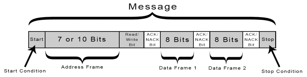
To explain it very briefly, START condition is when SDA becomes low while SCL is high. STOP condition is when SDA becomes high while SCL is high. Write bit is 0(Master will send data) while read bit is one(Slave will send the data). Last bit must be zero which signifies Slave has acknowledge/ACK the command, otherwise NACK which means there is a problem on the communication. Checking the ACK bit is the easiest way to know if Slave is active and is responding to your call.
And that is all there is need to know about I2C. Below is my I2C driver implementation in Verilog HDL,
`timescale 1ns / 1ps

module i2c_top //works on both i2c and SCCB mode(no pullups resistors needed) [NO REPEATED START ALLOWED]
	#(parameter main_clock=25_000_000, freq=100_000, addr_bytes=2) //addr_bytes=number of bytes of an address
	(
	input wire clk, rst_n,
	input wire start,stop,
	input wire[7:0] wr_data,
	output reg rd_tick, //ticks when read data from servant is ready,data will be taken from rd_data
	output reg[1:0] ack, //ack[1] ticks at the ack bit[9th bit],ack[0] asserts when ack bit is ACK,else NACK
	output wire[7:0] rd_data,
	inout scl,sda,
	output wire[3:0] state
    );

	 /*
	 i2c_top #(.freq(100_000)) m0
	(
		.clk(clk),
		.rst_n(rst_n),
		.start(start),
		.stop(stop),
		.wr_data(wr_data),
		.rd_tick(rd_tick), //ticks when read data from servant is ready,data will be taken from rd_data
		.ack(ack), //ack[1] ticks at the ack bit[9th bit],ack[0] asserts when ack bit is ACK,else NACK
		.rd_data(rd_data),
		.scl(scl),
		.sda(sda)
    );
	 */

	 localparam full= (main_clock)/(2*freq),
					half= full/2,
					counter_width=log2(full);
	 function integer log2(input integer n); //automatically determines the width needed by counter
		integer i;
		 begin
			log2=1;
			for(i=0;2**i<n;i=i+1)
				log2=i+1;
		 end
	 endfunction

	 //FSM state declarations
	 localparam[3:0] 		idle=0,
							starting=1,
							packet=2,
							ack_servant=3,
							read=4,
							ack_master=5,
							stop_1=6,
							stop_2=7;
	 reg[3:0] state_q=idle,state_d;
	 reg op_q=0,op_d;
	 reg[3:0] idx_q=0,idx_d;
	 reg[8:0] wr_data_q=0,wr_data_d;
	 reg[7:0] rd_data_q,rd_data_d;
	 reg scl_q=0,scl_d;
	 reg sda_q=0,sda_d;
	 reg[counter_width-1:0] counter_q=0,counter_d;
	 reg[1:0] addr_bytes_q=0,addr_bytes_d;
	 wire scl_lo,scl_hi;
	 wire sda_in;
	//register operations
	 always@(posedge clk, negedge rst_n) begin
		if(!rst_n) begin
			state_q<=idle;
			idx_q<=0;
			wr_data_q<=0;
			scl_q<=0;
			sda_q<=0;
			counter_q<=0;
			rd_data_q<=0;
			addr_bytes_q<=0;
		end
		else begin
			state_q<=state_d;
			op_q<=op_d;
			idx_q<=idx_d;
			wr_data_q<=wr_data_d;
			scl_q<=scl_d;
			sda_q<=sda_d;
			counter_q<=counter_d;
			rd_data_q<=rd_data_d;
			addr_bytes_q<=addr_bytes_d;
		end
	 end


	 //free-running clk, freq depends on parameter "freq"
	 always @* begin
		counter_d=counter_q+1;
		scl_d=scl_q;
		if(state_q==idle || state_q==starting) scl_d=1'b1;
		else if(counter_q==full) begin
			counter_d=0;
			scl_d=(scl_q==0)?1'b1:1'b0;
		end
	 end


	 //FSM next-state logic
	 always @* begin
		state_d=state_q;
		op_d=op_q;
		idx_d=idx_q;
		wr_data_d=wr_data_q;
		rd_data_d=rd_data_q;
		addr_bytes_d=addr_bytes_q;
		sda_d=sda_q;
		ack=0;
		rd_tick=0;

		case(state_q)
					idle: begin		//wait for the "start" to assert
								sda_d=1'b1;
								addr_bytes_d=addr_bytes;
								if(start==1'b1) begin
									wr_data_d={wr_data,1'b1}; //the last 1'b1 is for the ACK coming from the servant("1" means high impedance or "reading")
									op_d= (wr_data[0])? 1:0; // if last bit(R/W bit) is one:read operation, else write operation
									idx_d=8; //index to be used on transmitting the wr_data serially(MSB first)
									state_d=starting;
								end
							 end

				starting: if(scl_hi) begin //start command, change sda to low while scl is high
								sda_d=0;
								state_d=packet;
							 end

				  packet: if(scl_lo) begin //transmit wr_data serially(MSB first)
								sda_d= (wr_data_q[idx_q]==0)? 0:1'b1;
								idx_d= idx_q-1;
								if(idx_q==0) begin
									state_d=ack_servant;
									idx_d=0;
								end
							 end

			ack_servant: if(scl_hi) begin //wait for ACK bit response(9th bit) from servant
								ack[1]=1;
								ack[0]=!sda_in;
								wr_data_d={wr_data,1'b1}; //after acknowledge tick, master must have already have the next data it wants to give
								addr_bytes_d=addr_bytes_q-1;
								if(stop) state_d=stop_1; //master can forcefully stops the transaction(even if response is either NACK or ACK)
								else if(op_q && addr_bytes_q==0) begin //start reading after writing addr_bytes of packets for address
									idx_d=7;
									state_d=read;
								end
								else begin //write next packet
									idx_d=8;
									state_d=packet;
								end
							 end

					 read: if(scl_hi) begin //read data from slave(MSB first)
								rd_data_d[idx_q]=sda_in;
								idx_d=idx_q-1;
								if(idx_q==0) state_d=ack_master;
							 end

			 ack_master: if(scl_lo) begin //master must ACK after receiving data from servant
								sda_d=1'b0;
								if(sda_q==0) begin //one whole bit(two scl_lo) had passed
									rd_tick=1;
									idx_d=7;
									if(stop) state_d=stop_1; //after receiving data, master can opt to stop
									else state_d=read; ///after receiving data, master can also just continue receving more data
								end
							 end
				  stop_1: if(scl_lo) begin
								sda_d=1'b0;
								state_d=stop_2;
							 end
				  stop_2: if(scl_hi) begin
								sda_d=1'b1;
								state_d=idle;
							 end
				 default: state_d=idle;
		endcase
	 end

	 /*
	 //i2c output logic
	 assign scl=scl_q? 1'bz:0; //bidiectional logic for pull-up scl
	 assign sda=sda_q? 1'bz:0; //bidirectional logic for pull-up scl
	 assign sda_in=sda;
	 */

	 //sccb output logic
	 assign scl=scl_q; //sccb scl does not need pull-up
	 assign sda=(state_q==read || state_q==ack_servant)? 1'bz : sda_q; //sccb sda does not need pull-up
	 assign sda_in=sda;

	 /*
	 TRELLIS_IO #(.DIR("BIDIR")) tristate
	 (
	  .B(sda),
	  .I(sda_q),
	  .T(temp),
	  .O(sda_in)
	 );*/

	 assign scl_hi= scl_q==1'b1 && counter_q==half && scl==1'b1; //scl is on the middle of a high(1) bit
	 assign scl_lo= scl_q==1'b0 && counter_q==half; //scl is on the middle of a low(0) bit
	 assign rd_data=rd_data_q;
	 assign state=state_q;

endmodule
This I2C driver can be set to any frequency by setting the freq and main_clock.
I2C vs SCCB
Now, what is the difference between the two? Pull-up resistors. If you had played with I2C before, you would know that I2C need pull-ups. In I2C, the Master and Slave never produce a logic 1. It is just either low or high-impedance. High-impedance would be perceived as high by the receiving end because of the pull-ups. But in SCCB, the Master and Slave can produce all three states (high, low, and high-impedance) so there will be no need for pull-up resistors. In my I2C driver, you can choose either SCCB or I2C to use as you can see on the last part of the code (I2C is commented here):
     /*
	 //i2c output logic
	 assign scl=scl_q? 1'bz:0; //bidiectional logic for pull-up scl
	 assign sda=sda_q? 1'bz:0; //bidirectional logic for pull-up scl
	 assign sda_in=sda;
	 */

	 //sccb output logic
	 assign scl=scl_q; //sccb scl does not need pull-up
	 assign sda=(state_q==read || state_q==ack_servant)? 1'bz : sda_q; //sccb sda does not need pull-up
	 assign sda_in=sda;
OV7670 Initialization Sequence
Initialization of the OV7670 camera is very similar to SD card wherein we will need to send some commands to to set its parameters. There are a LOT of control registers we need to set and it will be exhaustive to list and explain it all here. You can access the list of device control register on this pdf (page 11 to 26).
Retrieving Pixel Data
After the initialization sequence, we can now retrieve the pixel data from the camera. This is where the most of the pins of the OV7670 is allocated for. As you might have guessed, pins D0-to-D7 are the pixel data in parallel(1 byte). This pixel data is synchronized to the PCLK coming from the camera. But before PCLK can run, the OV7670 must first have an input clock where the PCLK will be referenced to. And that is what the XCLK is for. The maximum frequency for XCLK is 25MHz.
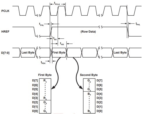
As we can see above, a single pixel has 16 bits (2 bytes) corresponding to RGB565 (5 bits red, 6 bits green, and 5 bits blue for a total of 16 bits). Each data bytes are synchronized to the falling edges of the PCLK (data is stable at rising edges). Since a single pixel has two bytes, two cycles of PCLK are needed to retrieve a single pixel. We just have to continue polling the PCLK pin to detect the rising edges and then store the data pixels. Take note that data pixels are valid if and only if HREF is high. When a frame of 640x480 ended, VSYNC will go high and when the camera is about to start a new frame, VSYNC will go low.
And that is all there is need to know about the basic interfacing with OV7670 camera, here is my camera driver in Verilog HDL,
`timescale 1ns / 1ps

  module camera_interface(
	input wire clk,rst_n, //100MHz clk
	input start_camera, //flag for starting the camera
	//triggers to start camera saving
	input btn,
	input pir_sensor,sound_sensor, temp_sensor,
	//camera fifo IO
	input wire rd_en,
	output empty,
	output wire[7:0] dout,
	//camera pinouts
	input wire cmos_pclk,cmos_href,cmos_vsync,
	input wire[7:0] cmos_db,
	inout cmos_sda,cmos_scl, //i2c comm wires
	output wire cmos_rst_n, cmos_pwdn, cmos_xclk,
	//Debugging
	output wire[3:0] led
    );
	 //FSM state declarations
	 localparam idle=0,
					start_sccb=1,
					write_address=2,
					write_data=3,
					digest_loop=4,
					delay=5,
					vsync_fedge=6,
					byte1=7,
					byte2=8,
					fifo_write=9,
					stopping=10,
					rest=11;

	 localparam wait_init=0,
					sccb_idle=1,
					sccb_address=2,
					sccb_data=3,
					sccb_stop=4;

	 localparam MSG_INDEX=77; //number of the last index to be digested by SCCB


	 reg[3:0] state_q=0,state_d;
	 reg[2:0] sccb_state_q=0,sccb_state_d;
	 reg[7:0] addr_q,addr_d;
	 reg[7:0] data_q,data_d;
	 reg[7:0] brightness_q,brightness_d;
	 reg[7:0] contrast_q,contrast_d;
	 reg start,stop;
	 reg[7:0] wr_data;
	 reg[3:0] led_q=0,led_d;
	 reg[27:0] delay_q=0,delay_d;
	 reg start_delay_q=0,start_delay_d;
	 reg delay_finish;
	 reg[15:0] message[250:0];
	 reg[7:0] message_index_q=0,message_index_d;
	 reg[15:0] pixel_q,pixel_d;
	 reg wr_en;
	 reg[7:0] gray_pixel_q=0,gray_pixel_d;
	 reg mod2_q=0,mod2_d;
	 reg[2:0] lines_q,lines_d;
	 reg[7:0] gray;
	 wire rd_tick;
	 wire[1:0] ack;
	 wire[7:0] rd_data;
	 wire[3:0] state;
	 wire full;
	 wire key0_tick,key1_tick,key2_tick,key3_tick;

	 reg[18:0] count_q=0,count_d;


	 //buffer for all inputs coming from the camera
	 reg pclk_1,pclk_2,href_1,href_2,vsync_1,vsync_2;


	 initial begin //collection of all adddresses and values to be written in the camera
				//{address,data}
	 message[0]=16'h12_80;  //reset all register to default values
	 message[1]=16'h12_04;  //set output format to RGB
	 message[2]=16'h15_20;  //pclk will not toggle during horizontal blank
	 message[3]=16'h40_d0;	//RGB565

	// These are values scalped from https://github.com/jonlwowski012/OV7670_NEXYS4_Verilog/blob/master/ov7670_registers_verilog.v
    message[4]= 16'h12_04; // COM7,     set RGB color output
    message[5]= 16'h11_80; // CLKRC     internal PLL matches input clock
    message[6]= 16'h0C_00; // COM3,     default settings
    message[7]= 16'h3E_00; // COM14,    no scaling, normal pclock
    message[8]= 16'h04_00; // COM1,     disable CCIR656
    message[9]= 16'h40_d0; //COM15,     RGB565, full output range
    message[10]= 16'h3a_04; //TSLB       set correct output data sequence (magic)
	 message[11]= 16'h14_18; //COM9       MAX AGC value x4 0001_1000
    message[12]= 16'h4F_B3; //MTX1       all of these are magical matrix coefficients
    message[13]= 16'h50_B3; //MTX2
    message[14]= 16'h51_00; //MTX3
    message[15]= 16'h52_3d; //MTX4
    message[16]= 16'h53_A7; //MTX5
    message[17]= 16'h54_E4; //MTX6
    message[18]= 16'h58_9E; //MTXS
    message[19]= 16'h3D_C0; //COM13      sets gamma enable, does not preserve reserved bits, may be wrong?
    message[20]= 16'h17_14; //HSTART     start high 8 bits
    message[21]= 16'h18_02; //HSTOP      stop high 8 bits //these kill the odd colored line
    message[22]= 16'h32_80; //HREF       edge offset
    message[23]= 16'h19_03; //VSTART     start high 8 bits
    message[24]= 16'h1A_7B; //VSTOP      stop high 8 bits
    message[25]= 16'h03_0A; //VREF       vsync edge offset
    message[26]= 16'h0F_41; //COM6       reset timings
    message[27]= 16'h1E_00; //MVFP       disable mirror / flip //might have magic value of 03
    message[28]= 16'h33_0B; //CHLF       //magic value from the internet
    message[29]= 16'h3C_78; //COM12      no HREF when VSYNC low
    message[30]= 16'h69_00; //GFIX       fix gain control
    message[31]= 16'h74_00; //REG74      Digital gain control
    message[32]= 16'hB0_84; //RSVD       magic value from the internet *required* for good color
    message[33]= 16'hB1_0c; //ABLC1
    message[34]= 16'hB2_0e; //RSVD       more magic internet values
    message[35]= 16'hB3_80; //THL_ST
    //begin mystery scaling numbers
    message[36]= 16'h70_3a;
    message[37]= 16'h71_35;
    message[38]= 16'h72_11;
    message[39]= 16'h73_f0;
    message[40]= 16'ha2_02;
    //gamma curve values
    message[41]= 16'h7a_20;
    message[42]= 16'h7b_10;
    message[43]= 16'h7c_1e;
    message[44]= 16'h7d_35;
    message[45]= 16'h7e_5a;
    message[46]= 16'h7f_69;
    message[47]= 16'h80_76;
    message[48]= 16'h81_80;
    message[49]= 16'h82_88;
    message[50]= 16'h83_8f;
    message[51]= 16'h84_96;
    message[52]= 16'h85_a3;
    message[53]= 16'h86_af;
    message[54]= 16'h87_c4;
    message[55]= 16'h88_d7;
    message[56]= 16'h89_e8;
    //AGC and AEC
    message[57]= 16'h13_e0; //COM8, disable AGC / AEC
    message[58]= 16'h00_00; //set gain reg to 0 for AGC
    message[59]= 16'h10_00; //set ARCJ reg to 0
    message[60]= 16'h0d_40; //magic reserved bit for COM4
    message[61]= 16'h14_18; //COM9, 4x gain + magic bit
    message[62]= 16'ha5_05; // BD50MAX
    message[63]= 16'hab_07; //DB60MAX
    message[64]= 16'h24_95; //AGC upper limit
    message[65]= 16'h25_33; //AGC lower limit
    message[66]= 16'h26_e3; //AGC/AEC fast mode op region
    message[67]= 16'h9f_78; //HAECC1
    message[68]= 16'ha0_68; //HAECC2
    message[69]= 16'ha1_03; //magic
    message[70]= 16'ha6_d8; //HAECC3
    message[71]= 16'ha7_d8; //HAECC4
    message[72]= 16'ha8_f0; //HAECC5
    message[73]= 16'ha9_90; //HAECC6
    message[74]= 16'haa_94; //HAECC7
    message[75]= 16'h13_e5; //COM8, enable AGC / AEC
	// message[76]= 16'h1E_23; //Mirror Image
	 message[77]= 16'h69_06; //gain of RGB(manually adjusted)
  end

	 //register operations
	 always @(posedge clk,negedge rst_n) begin
		if(!rst_n) begin
			state_q<=0;
			led_q<=0;
			delay_q<=0;
			start_delay_q<=0;
			message_index_q<=0;
			pixel_q<=0;
			gray_pixel_q<=0;

			sccb_state_q<=0;
			addr_q<=0;
			data_q<=0;
			brightness_q<=0;
			contrast_q<=0;
			mod2_q<=0;
			count_q<=0;
			lines_q<=0;
		end
		else begin
			state_q<=state_d;
			led_q<=led_d;
			delay_q<=delay_d;
			start_delay_q<=start_delay_d;
			message_index_q<=message_index_d;
			pclk_1<=cmos_pclk;
			pclk_2<=pclk_1;
			href_1<=cmos_href;
			href_2<=href_1;
			vsync_1<=cmos_vsync;
			vsync_2<=vsync_1;
			pixel_q<=pixel_d;

			gray_pixel_q<=gray_pixel_d;
			sccb_state_q<=sccb_state_d;
			addr_q<=addr_d;
			data_q<=data_d;
			brightness_q<=brightness_d;
			contrast_q<=contrast_d;
			mod2_q<=mod2_d;
			count_q<=count_d;
			lines_q<=lines_d;
		end
	 end


	 //FSM next-state logics
	 always @* begin
		state_d=state_q;
		led_d=led_q;
		start=0;
		stop=0;
		wr_data=0;
		start_delay_d=start_delay_q;
		delay_d=delay_q;
		delay_finish=0;
		message_index_d=message_index_q;
		pixel_d=pixel_q;
		gray_pixel_d=gray_pixel_q;
		lines_d=lines_q;
		wr_en=0;

		sccb_state_d=sccb_state_q;
		addr_d=addr_q;
		data_d=data_q;
		brightness_d=brightness_q;
		contrast_d=contrast_q;
		mod2_d=mod2_q;
		count_d=count_q;

		//delay logic
		if(start_delay_q) delay_d=delay_q+1'b1;
		if(delay_q[16] && message_index_q!=(MSG_INDEX+1) && (state_q!=start_sccb))  begin  //delay between SCCB transmissions (0.66ms)
			delay_finish=1;
			start_delay_d=0;
			delay_d=0;
		end
		else if((delay_q[26] && message_index_q==(MSG_INDEX+1)) || (delay_q[26] && state_q==start_sccb)) begin //delay BEFORE SCCB transmission, AFTER SCCB transmission, and BEFORE retrieving pixel data from camera (0.67s)
			delay_finish=1;
			start_delay_d=0;
			delay_d=0;
		end

		case(state_q)

					////////Begin: Setting register values of the camera via SCCB///////////

			  idle:  if(delay_finish && start_camera) begin //idle for 0.6s to start-up the camera
							state_d=start_sccb;
							start_delay_d=0;
							count_d=0;
							lines_d=0;
							led_d=4'b1000;
						end
						else start_delay_d=1;

		start_sccb:  begin   //start of SCCB transmission
							start=1;
							wr_data=8'h42; //slave address of OV7670 for write
							state_d=write_address;
							led_d=4'b1100;
						end
	 write_address: if(ack==2'b11) begin
							wr_data=message[message_index_q][15:8]; //write address
							state_d=write_data;
							led_d=4'b1110;
						end
		 write_data: if(ack==2'b11) begin
							wr_data=message[message_index_q][7:0]; //write data
							state_d=digest_loop;
						end
	  digest_loop: if(ack==2'b11) begin //stop sccb transmission
							stop=1;
							start_delay_d=1;
							message_index_d=message_index_q+1'b1;
							state_d=delay;
						end
			  delay: begin
							if(message_index_q==(MSG_INDEX+1) && delay_finish) begin
								state_d=rest; //if all messages are already digested, proceed to retrieving camera pixel data
								mod2_d=0;
								led_d=4'b1111; //red LEDs
							end
							else if(state==0 && delay_finish) state_d=start_sccb; //small delay before next SCCB transmission(if all messages are not yet digested)
						end


				///////////////Begin: Retrieving Pixel Data from Camera to be Stored to SDRAM/////////////////
			   rest: if(key_tick || pir_sensor || !sound_sensor || temp_sensor) begin
			             lines_d=0;
			             state_d=vsync_fedge;
			         end
		vsync_fedge: begin
                        if(vsync_1==0 && vsync_2==1 && empty && lines_q<5) begin
                              lines_d=lines_q+1;
                              state_d=byte1; //vsync falling edge means new frame is incoming
                              count_d=0;
                         end
                         else if(lines_q==5) begin
                                     state_d=rest;
                                     led_d=4'b0110;
                         end
                      end
				byte1: if(pclk_1==1 && pclk_2==0 && href_1==1 && href_2==1) begin //rising edge of pclk means new pixel data(first byte of 16-bit pixel RGB565) is available at output
								//pixel_d[15:8]=cmos_db;
								//state_d=byte2;
								///////////////
								case(lines_q)
								1:wr_en=count_q>=0 && count_q<=65535;
								2:wr_en=count_q>=65536 && count_q<=131071;
								3:wr_en=count_q>=131072 && count_q<=196607;
								4:wr_en=count_q>=196608 && count_q<=262143;
								5:wr_en=count_q>=262144 && count_q<=327679;
								endcase
                                state_d=byte2;
								///////////////
								led_d=4'b1001;
						 end
						 else if(vsync_1==1 && vsync_2==1) begin
							state_d=vsync_fedge;
						 end
				byte2: if(pclk_1==1 && pclk_2==0 && href_1==1 && href_2==1) begin //rising edge of pclk means new pixel data(second byte of 16-bit pixel RGB565) is available at output
								//pixel_d[7:0]=cmos_db;
								//state_d=fifo_write;
								case(lines_q)
								1:wr_en=count_q>=0 && count_q<=65535;
								2:wr_en=count_q>=65536 && count_q<=131071;
								3:wr_en=count_q>=131072 && count_q<=196607;
								4:wr_en=count_q>=196608 && count_q<=262143;
								5:wr_en=count_q>=262144 && count_q<=327679;
								endcase
                                state_d=byte1;
                                count_d=(count_q<307200)? (count_q+1'b1):count_q;
						 end
						 else if(vsync_1==1 && vsync_2==1) begin
							state_d=vsync_fedge;
						 end
		 /*fifo_write: begin //write the 16-bit data to asynchronous fifo to be retrieved later by SDRAM
								state_d=byte1;
								////////////////////////////
								gray=(pixel_q[15:11]+(pixel_q[10:5]>>1)+pixel_q[4:0])/3; //RGB to grayscale conversion using averaging method
								gray_pixel_d={gray_pixel_q[3:0],gray[3:0]};
								mod2_d=mod2_q+1;
								wr_en=(mod2_q==1) && count_q<256000; //save data when two gray pixel(8 bytes) are saved on gray_pixel_q;
								led_d=wr_en? 4'b1001:4'b0110;
						 end*/
		default: state_d=idle;
		endcase

		/*
		//Logic for increasing/decreasing brightness and contrast via the 4 keybuttons
		case(sccb_state_q)
			wait_init: if(state_q==byte1) begin //wait for initial SCCB transmission to finish
							sccb_state_d=sccb_idle;
							addr_d=0;
							data_d=0;
							brightness_d=8'h00;
							contrast_d=8'h40;
						  end
			sccb_idle: if(state==0) begin //wait for any pushbutton
								if(key0_tick) begin//increase brightness
									brightness_d=(brightness_q[7]==1)? brightness_q-5:brightness_q+5;
									if(brightness_q==8'h80) brightness_d=0;
									start=1;
									wr_data=8'h42; //slave address of OV7670 for write
									addr_d=8'h55; //brightness control address
									data_d=brightness_d;
									sccb_state_d=sccb_address;
									led_d=0;
								end
								if(key1_tick) begin //decrease brightness
									brightness_d=(brightness_q[7]==1)? brightness_q+5:brightness_q-5;
									if(brightness_q==0) brightness_d=8'h80;
									start=1;
									wr_data=8'h42;
									addr_d=8'h55;
									data_d=brightness_d;
									sccb_state_d=sccb_address;
									led_d=0;
								end
								else if(key2_tick) begin //increase contrast
									contrast_d=contrast_q+5;
									start=1;
									wr_data=8'h42; //slave address of OV7670 for write
									addr_d=8'h56; //contrast control address
									data_d=contrast_d;
									sccb_state_d=sccb_address;
									led_d=0;
								end
								else if(key3_tick) begin //decrease contrast
									contrast_d=contrast_q-5;
									start=1;
									wr_data=8'h42;
									addr_d=8'h56;
									data_d=contrast_d;
									sccb_state_d=sccb_address;
									led_d=0;
								end
						  end
		sccb_address: if(ack==2'b11) begin
							wr_data=addr_q; //write address
							sccb_state_d=sccb_data;
						end
		  sccb_data: if(ack==2'b11) begin
							wr_data=data_q; //write databyte
							sccb_state_d=sccb_stop;
						 end
		  sccb_stop: if(ack==2'b11) begin //stop
							stop=1;
							sccb_state_d=sccb_idle;
							led_d=4'b1001;
						 end
			 default: sccb_state_d=wait_init;
		endcase
		*/
		//debug
		/*if(count_q<38400) pixel_d={{5{1'b0}},{6{1'b0}},{5{1'b0}}};
		else if(count_q<76800) pixel_d={{5{1'b0}},{6{1'b0}},{5{1'b1}}};
		else if(count_q<115200) pixel_d={{5{1'b0}},{6{1'b1}},{5{1'b0}}};
		else if(count_q<153600) pixel_d={{5{1'b0}},{6{1'b1}},{5{1'b1}}};
		else if(count_q<192000) pixel_d={{5{1'b1}},{6{1'b0}},{5{1'b0}}};
		else if(count_q<230400) pixel_d={{5{1'b1}},{6{1'b0}},{5{1'b1}}};
		else if(count_q<268800) pixel_d={{5{1'b1}},{6{1'b1}},{5{1'b0}}};
		else if(count_q<307200) pixel_d={{5{1'b1}},{6{1'b1}},{5{1'b1}}};*/
	 end


	 assign cmos_pwdn=0;
	 assign cmos_rst_n=1;
	 assign led=led_q;

	 //module instantiations
	 i2c_top #(.main_clock(100_000_000), .freq(100_000)) m0
	(
		.clk(clk),
		.rst_n(rst_n),
		.start(start),
		.stop(stop),
		.wr_data(wr_data),
		.rd_tick(rd_tick), //ticks when read data from servant is ready,data will be taken from rd_data
		.ack(ack), //ack[1] ticks at the ack bit[9th bit],ack[0] asserts when ack bit is ACK,else NACK
		.rd_data(rd_data),
		.scl(cmos_scl),
		.sda(cmos_sda),
		.state(state)
    );


	assign cmos_xclk=clk;


	asyn_fifo #(.DATA_WIDTH(8),.FIFO_DEPTH_WIDTH(17)) m2 //2048x8 FIFO mem
	(
		.rst_n(rst_n),
		.clk_write(clk),
		.clk_read(clk), //clock input from both domains
		.write(wr_en),
		.read(rd_en),
		//.data_write(gray_pixel_q), //input FROM write clock domain
		.data_write(cmos_db),
		.data_read(dout), //output TO read clock domain
		.full(full),
		.empty(empty) //full=sync to write domain clk , empty=sync to read domain clk
		//.data_count_r()
    );

debounce_explicit m3
	(
		.clk(clk),
		.rst_n(rst_n),
		.sw(btn),
		.db_level(),
		.db_tick(key_tick)
    );

endmodule
If you try to read the code, you will notice that I instantiated an asynchronous FIFO (First-in First-out) module. FIFO simply acts as a buffer for the data pixels coming from the camera.
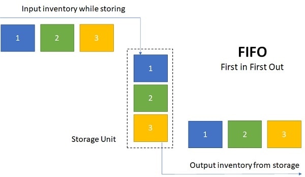
There are two types of FIFO, synchronous and asynchronous FIFO. The difference is that asynchronous FIFO have separate clock domains for read and write. Asynchronous FIFO is what I used here so that it will be much more flexible. This means the receiving end of the data pixels does not need to have the same clock frequency as the camera_interface module.
Here is my asynchronous FIFO module in Verilog HDL,
`timescale 1ns / 1ps

module asyn_fifo
	#(
		parameter DATA_WIDTH=8,
					 FIFO_DEPTH_WIDTH=11  //total depth will then be 2**FIFO_DEPTH_WIDTH
	)
	(
	input wire rst_n,
	input wire clk_write,clk_read, //clock input from both domains
	input wire write,read,
	input wire [DATA_WIDTH-1:0] data_write, //input FROM write clock domain
	output wire [DATA_WIDTH-1:0] data_read, //output TO read clock domain
	output reg full,empty //full=sync to write domain clk , empty=sync to read domain clk
	//output reg[FIFO_DEPTH_WIDTH-1:0] data_count_w,data_count_r //counts number of data left in fifo memory(sync to either write or read clk)
    );


	 /*
	 async_fifo #(.DATA_WIDTH(16),.FIFO_DEPTH_WIDTH(10)) m2 //1024x16 FIFO mem
	(
		.rst_n(rst_n),
		.clk_write(),
		.clk_read(), //clock input from both domains
		.write(),
		.read(),
		.data_write(), //input FROM write clock domain
		.data_read(), //output TO read clock domain
		.full(),
		.empty(), //full=sync to write domain clk , empty=sync to read domain clk
		..data_count_w(),
		.data_count_r() //counts number of data left in fifo memory(sync to either write or read clk)
    );
	 */


	 localparam FIFO_DEPTH=2**FIFO_DEPTH_WIDTH;

	 initial begin
		full=0;
		empty=1;
	 end


	 ///////////////////WRITE CLOCK DOMAIN//////////////////////////////
	 reg[FIFO_DEPTH_WIDTH:0] w_ptr_q=0; //binary counter for write pointer
	 reg[FIFO_DEPTH_WIDTH:0] r_ptr_sync; //binary pointer for read pointer sync to write clk
	 wire[FIFO_DEPTH_WIDTH:0] w_grey,w_grey_nxt; //grey counter for write pointer
	 reg[FIFO_DEPTH_WIDTH:0] r_grey_sync; //grey counter for the read pointer synchronized to write clock

	 wire we;
	 reg[5:0] i; //log_2(FIFO_DEPTH_WIDTH)

	 assign w_grey=w_ptr_q^(w_ptr_q>>1); //binary to grey code conversion for current write pointer
	 assign w_grey_nxt=(w_ptr_q+1'b1)^((w_ptr_q+1'b1)>>1);  //next grey code
	 assign we= write && !full;

	 //register operation
	 always @(posedge clk_write,negedge rst_n) begin
		if(!rst_n) begin
			w_ptr_q<=0;
			full<=0;
		end
		else begin
			if(write && !full) begin //write condition
				w_ptr_q<=w_ptr_q+1'b1;
				full <= w_grey_nxt == {~r_grey_sync[FIFO_DEPTH_WIDTH:FIFO_DEPTH_WIDTH-1],r_grey_sync[FIFO_DEPTH_WIDTH-2:0]}; //algorithm for full logic which can be observed on the grey code table
			end
			else full <= w_grey == {~r_grey_sync[FIFO_DEPTH_WIDTH:FIFO_DEPTH_WIDTH-1],r_grey_sync[FIFO_DEPTH_WIDTH-2:0]};

			for(i=0;i<=FIFO_DEPTH_WIDTH;i=i+1) r_ptr_sync[i]=^(r_grey_sync>>i); //grey code to binary converter
			//data_count_w <= (w_ptr_q>=r_ptr_sync)? (w_ptr_q-r_ptr_sync):(FIFO_DEPTH-r_ptr_sync+w_ptr_q); //compares write pointer and sync read pointer to generate data_count
		end
	 end

	/////////////////////////////////////////////////////////////////////


	  ///////////////////READ CLOCK DOMAIN//////////////////////////////
	 reg[FIFO_DEPTH_WIDTH:0] r_ptr_q=0; //binary counter for read pointer
	 wire[FIFO_DEPTH_WIDTH:0] r_ptr_d;
	 reg[FIFO_DEPTH_WIDTH:0] w_ptr_sync; //binary counter for write pointer sync to read clk
	 reg[FIFO_DEPTH_WIDTH:0] w_grey_sync; //grey counter for the write pointer synchronized to read clock
	 wire[FIFO_DEPTH_WIDTH:0] r_grey,r_grey_nxt; //grey counter for read pointer


	 assign r_grey= r_ptr_q^(r_ptr_q>>1);  //binary to grey code conversion
	 assign r_grey_nxt= (r_ptr_q+1'b1)^((r_ptr_q+1'b1)>>1); //next grey code
	 assign r_ptr_d= (read && !empty)? r_ptr_q+1'b1:r_ptr_q;

	 //register operation
	 always @(posedge clk_read,negedge rst_n) begin
		if(!rst_n) begin
			r_ptr_q<=0;
			empty<=1;
		end
		else begin
			r_ptr_q<=r_ptr_d;
			if(read && !empty) empty <= r_grey_nxt==w_grey_sync;//empty condition
			else empty <= r_grey==w_grey_sync;

			for(i=0;i<=FIFO_DEPTH_WIDTH;i=i+1) w_ptr_sync[i]=^(w_grey_sync>>i); //grey code to binary converter
			//data_count_r = (w_ptr_q>=r_ptr_sync)? (w_ptr_q-r_ptr_sync):(FIFO_DEPTH-r_ptr_sync+w_ptr_q); //compares read pointer to sync write pointer to generate data_count
		end
	 end
	 ////////////////////////////////////////////////////////////////////////


	 /////////////////////CLOCK DOMAIN CROSSING//////////////////////////////
	 reg[FIFO_DEPTH_WIDTH:0] r_grey_sync_temp;
	 reg[FIFO_DEPTH_WIDTH:0] w_grey_sync_temp;
	 always @(posedge clk_write) begin //2 D-Flipflops for reduced metastability in clock domain crossing from READ DOMAIN to WRITE DOMAIN
		r_grey_sync_temp<=r_grey;
		r_grey_sync<=r_grey_sync_temp;
	 end
	 always @(posedge clk_read) begin //2 D-Flipflops for reduced metastability in clock domain crossing from WRITE DOMAIN to READ DOMAIN
		w_grey_sync_temp<=w_grey;
		w_grey_sync<=w_grey_sync_temp;
	 end

	//////////////////////////////////////////////////////////////////////////


	//instantiation of dual port block ram
	dual_port_sync #(.ADDR_WIDTH(FIFO_DEPTH_WIDTH) , .DATA_WIDTH(DATA_WIDTH)) m0
	(
		.clk_r(clk_read),
		.clk_w(clk_write),
		.we(we),
		.din(data_write),
		.addr_a(w_ptr_q[FIFO_DEPTH_WIDTH-1:0]), //write address
		.addr_b(r_ptr_d[FIFO_DEPTH_WIDTH-1:0] ), //read address ,addr_b is already buffered inside this module so we will use the "_d" ptr to advance the data(not "_q")
		.dout(data_read)
	);

endmodule


	//inference template for dual port block ram
module dual_port_sync
	#(
		parameter ADDR_WIDTH=11, //2k by 8 dual port synchronous ram(16k block ram)
					 DATA_WIDTH=8
	)
	(
		input clk_r,
		input clk_w,
		input we,
		input[DATA_WIDTH-1:0] din,
		input[ADDR_WIDTH-1:0] addr_a,addr_b, //addr_a for write, addr_b for read
		output[DATA_WIDTH-1:0] dout
	);

	reg[DATA_WIDTH-1:0] ram[2**ADDR_WIDTH-1:0];
	reg[ADDR_WIDTH-1:0] addr_b_q;

	always @(posedge clk_w) begin
		if(we) ram[addr_a]<=din;
	end
	always @(posedge clk_r) begin
		addr_b_q<=addr_b;
	end
	assign dout=ram[addr_b_q];

endmodule
Limitations and Bottlenecks
Now that our camera is ready for action, we can now connect it to the SD card driver. But before that, let us first talk about the the limitations we need to face for this project. Remember that the SD card in SPI mode are relatively much slower than your average SD card running in 4-bit SD mode, this means we cannot directly save videos on it just like a normal video camera. We can only capture images one at a time. The biggest bottleneck in saving images to the SD card is that the CMOD S7 only has 1620Kb of Block Ram. But if we compute the number of bits needed on a single frame of 640x480 image produced by OV7670:
16 bits/pixel * 640 pixels/line * 480 lines/frame =4915200 bits/frame
4915Kb! That is over 3 times of what the CMOD S7 FPGA board can handle. You might think that if we cannot store all one frame to the block ram, then why can't we just skip the block ram and save it directly to the SD card? The SD card is the final destination of the data so why bother storing it first to block ram? AHA! But unfortunately, that will not work because another bottleneck here is the busy time of the SD card after writing a block. Remember on my blog 2 that after writing 512 bytes, the SD card will be busy for some definite time and will hold the SD MISO low. In my SD card (32GB SDHC), busy time takes an average of 1ms. This means that no matter how fast I write the 512 bytes consecutively, I will always be limited to 1ms of write per 512 bytes. This means that in a second, the fastest I can write is:
512 bytes/1ms * 8 bits/byte =4096000 bits/sec
That is NOT enough to cover the whole frame! (4915200 bits). And remember that in one second we have 30 frames(30fps), this means that if we want to save all 30 frames we will need:
4915200 bits/frame * 30 frames/sec =147.46 Kb/sec or 18.4KBytes/sec
HOLY! That is already the speed of a normal SD card in 4-bit SD mode.
So, what should we do now?
Hmmmm, lets see. If we cannot save all 30 frames in one second then let us focus on saving at least one frame. And since the block ram cannot handle one whole frame, then we can just divide the frame into chunks!


SPOILER ALERT! The image above was captured using the OV7670 camera already. By the way, that is my press ball globe. On the left side, you might perceive it as 1 whole frame. But the truth is that this image consists of 5 frames already. On the right side, you can see that there are 5 chunks. Saving of image data goes like this: Block 1 was saved first. After saving we wait for another frame to save Block 2, after saving we wait again for another frame to save Block 3, and so on. Saving a single 640x480 image with 16 bits per pixel took 1.5 seconds for my 32Gb SD card.
That is my solution for the bottlenecks of this project (divide into chunks, save, then combine together), if you have better ways to do it just comment it down! Now, the code for this is simple, we just have to make the counters that will count in all 640*480=307200 pixels and then divide it by five. Each chunks will be saved to the asyn_fifo. The asyn_fifo has 17 bits for the address for a total of 2^17=131072 bytes of writable addresses. This is already 70% of the block ram of CMOD S7.The camera driver I showed to you earlier has already that modification, the main code that deals with dividing the frames into chunks is:
byte1: if(pclk_1==1 && pclk_2==0 && href_1==1 && href_2==1) begin //rising edge of pclk means new pixel data(first byte of 16-bit pixel RGB565) is available at output
		///////////////
		case(lines_q)
		1:wr_en=count_q>=0 && count_q<=65535;
		2:wr_en=count_q>=65536 && count_q<=131071;
		3:wr_en=count_q>=131072 && count_q<=196607;
		4:wr_en=count_q>=196608 && count_q<=262143;
		5:wr_en=count_q>=262144 && count_q<=327679;
		endcase
        state_d=byte2;
		///////////////
		led_d=4'b1001;
        end
Now, it's time to connect the camera driver and SD card driver. It's pretty straightforward since what we want to do is to trigger the SD card driver to start write operation as long as data is available at the asyn_fifo. This is the same as saying that SD card write operation should start only when asyn_fifo is not empty. Below is the top module that connects all drivers used (mainly the camera driver and SD card driver). Notice how I connected the invert of the empty pin of the camera_interface to the write pin of sdcard_interface:
`timescale 1ns / 1ps

module top_module(
    input clk,
    input rst,
    //triggers to start saving picture to sdcard
    input wire btn, //manual capture of camera
    input pir_sensor, sound_sensor, //peripherals
    //leds for debugging
    output wire led0_r,led0_g,led0_b, //{red,green,blue} red if SDCARD initialization is stuck at CMD0, blue if stuck somewhere else, green if initialization complete
    output wire[3:0] led , //4 leds on after sdcard initialization
    //SPI pinouts
	input wire SD_MISO,
	output wire SD_MOSI,
	output wire SD_DCLK,SD_nCS,
	//UART for debugging
	output wire uart_rx,uart_tx,
    //camera pinouts
	input wire cmos_pclk,cmos_href,cmos_vsync,
	input wire[7:0] cmos_db,
	inout cmos_sda,cmos_scl, //i2c comm wires
	output wire cmos_rst_n, cmos_pwdn, cmos_xclk,
	//Analog input
	input wire vaux5_p, vaux5_n //pin 32
    );


    localparam TEMP_LIMIT=50; //trigger camera when reached 30 degrees Celsius
    wire idle;
    wire empty,rd_en_cam;
    wire[7:0] dout_cam;
    wire[11:0] adc_1;
    wire[11:0] temp;

    //module instantiations
    sdcard_interface m0
    (
        .clk(clk_out),
        .rst(rst),
        .led0_r(led0_r),
        .led0_g(led0_g),
        .led0_b(led0_b), //{red,green,blue} red if SDCARD initialization is stuck at CMD0, blue if stuck somewhere else, green if initialization complete
        .idle(idle),  //sdcard not busy
         //HOST interface
        .write({!empty}),
        .rd_fifo(rd_en_cam),
        .data(dout_cam),
        //SPI pinouts
        .SD_MISO(SD_MISO),
        .SD_MOSI(SD_MOSI),
        .SD_DCLK(SD_DCLK),
        .SD_nCS(SD_nCS),
        //UART for debugging
        .uart_rx(uart_rx),
        .uart_tx(uart_tx)
    );

    camera_interface m1
    (
	    .clk(clk_out),
	    .rst_n({!rst}), //100MHz clk
	    .start_camera(idle),
	    //triggers to start camera saving
	    .pir_sensor(pir_sensor),
	    .sound_sensor(sound_sensor),
	    .temp_sensor(fire),
	    .btn(btn),
         //camera fifo IO
	    .rd_en(rd_en_cam),
	    .empty(empty),
	    .dout(dout_cam),
	     //camera pinouts
        .cmos_pclk(cmos_pclk),
        .cmos_href(cmos_href),
        .cmos_vsync(cmos_vsync),
	    .cmos_db(cmos_db),
	    .cmos_sda(cmos_sda),
	    .cmos_scl(cmos_scl), //i2c comm wires
	    .cmos_rst_n(cmos_rst_n),
	    .cmos_pwdn(cmos_pwdn),
	     //Debugging
	    .led(led)
    );

    xadc_interface m2
    ( //reads ADC output and store to register
        .clk(clk),
        .rst(rst),
        .vaux5_p(vaux5_p),
        .vaux5_n(vaux5_n), //pin 32
        .adc_1(adc_1) //ADC CODE: adc_0(die temp) , adc_1(pin 32) , adc_2(pin33)
    );


   clk_wiz_1 m3 //100MHz clk
   (
        // Clock out ports
        .clk_out1(clk_out),     //100MHz
        .clk_out2(cmos_xclk), //12MHz
       // Clock in ports
        .clk_in1(clk)
   );      // input clk_in1


    wire fire; //logic 1 if temp is abnormally high
    assign temp=adc_1/12; //temp in celsius = [(adc_1/4095)*3.3V]*100Cel/V
    assign fire=temp>TEMP_LIMIT;
    //assign led=fire? 4'b1111:0;

     //temperature sensor data extraction
    ila_0 your_instance_name (
	.clk(clk), // input wire clk
	.probe0(adc_1), // input wire [11:0]  probe0
	.probe1(temp), // input wire [7:0]  probe1
	.probe2(fire), // input wire [0:0]  probe2
	.probe3(led) // input wire [3:0]  probe3
);

endmodule
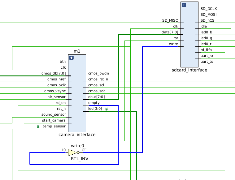
Below is the schematic for the connection of camera_interface and sdcard_interface,
Preview for the Next Blog
Now that the camera driver is connected to the SD card driver, are we finished already? NOT YET, because we are still missing the important pieces that will make this camera a real Security Camera. Next stop: adding peripheral sensors.
6-Part Blog Series
- Security Camera #1: Project Proposal
- Security Camera #2: SD Card Interfacing
- Security Camera #3: Testing the SD Card Driver
- Security Camera #4: Interfacing with OV7670 Camera
- Security Camera #5: Adding Peripheral Sensors
- Security Camera #6: Project Demonstration and Final Words
To see more of my FPGA projects, visit my GitHub account: https://github.com/AngeloJacobo
References
https://circuitdigest.com/microcontroller-projects/how-to-use-ov7670-camera-module-with-arduino
https://www.teachmemicro.com/arduino-camera-ov7670-tutorial/
https://www.circuitbasics.com/basics-of-the-i2c-communication-protocol/
https://www.circuitbasics.com/basics-of-the-i2c-communication-protocol/