Hello everyone. I welcome you to my 7th blog as part of Summer of Sensors Design Challenge and In the Air Tonight category. In my first blog I described plans as part of competition. In second blog I shown Evaluation Kit of ZMOD4510 Outdoor Air Quality. In third blog I shown software provided for evaluating the sensor. In forth blog I shown how easily integrate this sensor with Renesas RA2L1 Microcontroller. In fifth blog I described my journey when adding Renesas DA16600 Wi-Fi Module to the project for achieving Wi-Fi connectivity and finally, in previous (sixth) blog post I describe my box and my outdoor deployment of the project.
Today I will describe my results from my first outdoor deployment and its improvement.
Battery life
In previous blog post you have seen that for powering I used 3x AA batteries with nominal voltage 1.5V. They were connected in serie and powered onboard LDO which converted 5V (4.5V and less due to batteries) to 3.3V which was later used for powering RA2L1 MCU, onboard debugger MCU, ZMOD4510 sensor and Wi-Fi Module. As far I did only minor improvements like desoldering always-on LED. I estimated that everything will be fine because I used low-power MCU, low-power capable Wi-Fi module, low-power air quality sensor with low-power algorithm deployed on MCU and debugger MCU without any USB communication I estimated as also very low-power. But this was mistake and battery in this design was ruined out after first 6 hours of running. After aprox. 6 hours I received latest data and I noticed that MCU reboots frequently and debugger LED flashes less. Batteries voltage was 2.63V. This should be sufficient for all parts but most probably when Wi-Fi was transmitting data, power consumption grown, and voltage drop caused module instability and further issue.
Measuring Power Consumption
I considered battery life of 6 hours as a big failure, so I decided to take more advanced approach instead of opinion-based thoughts and decided to measure power consumption of whole device by amperemeter. For measuring I used USB current consumption measurement probe which I made as part of previous Experimenting with Current Sense Amplifiers project. Probe allowed me monitor current flowing through USB cable which was used for powering device. More details including schematics, board layout and detailed descriptions about this probe are in mentioned blog post.
With this setup I measured power consumption of whole device as 61.5 mA (note that I swapped red and black probe, so I was receiving negative values).
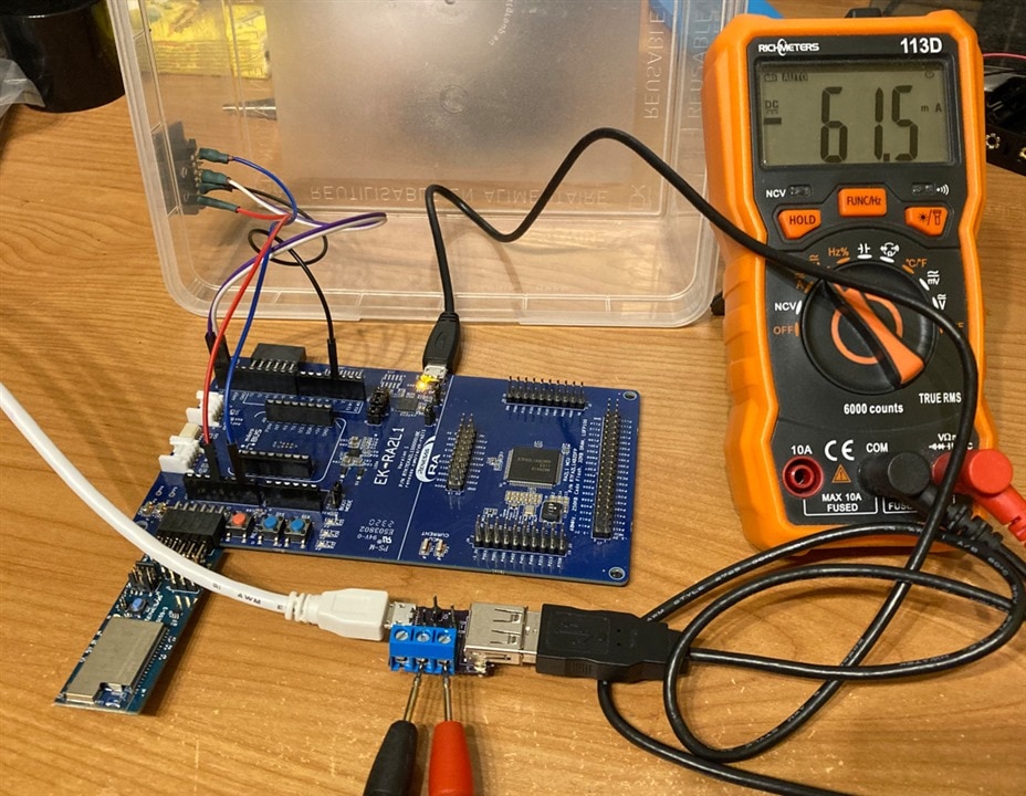
Power consumption without Wi-Fi
As the most power-hungry device I considered Wi-Fi module. For experiment I try disconnecting it. Power consumption dropped to 21.22 mA. After subtracting we get that Wi-Fi module consume the most energy (~40 mA).
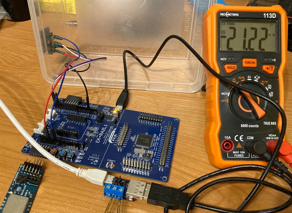
Power consumptions mentioned above were almost constant. Device consumed 61.5 mA for a whole time. There were no (visible) peaks or drops.
Remaining power consumption of about 21 mA is shared between:
- RA2L1 MCU
- J-Link OB Debugger + its LED
- ZMOD4510 sensor
- 5V -> 3.3V LDO quiescent current
Theoretical analysis
I analysed documentation to each part and take in account several ways how to reduce power consumption.
Optimization #1: DA16600 Wi-Fi Module
Reducing power consumption of module is hard. Originally, I developed way for powering-off module by N-MOS transistor. I added logic for buffering measured data in the RA2L1 MCU firmware. As far I sent to cloud immediately and now I send them to the cloud once per hour in batch. Power to module was cut-off by transistor at remaining time.
This solution was complicated because I had to change behaviour of all PMOD pins to Hi-Z (for preventing backpowering module from GPIO) and then drive transistor. On power on I had to restore GPIOs again and enable transistor. I also had to significantly change state machine of my driver for supporting this.
I also had to implement RTC logic for keeping time. When I was sending samples immediately, I just added timestamp at the upload time but now I need to timestamp samples at firmware because they are sent to the cloud in batch. Setting time is not manual task but instead I read time from Wi-Fi Module using AT command. Wi-Fi module runs NTP client. I sync time after every wi-fi reconnect.
This optimization helped me a lot, but I was still not satisfied and continued thinking about other parts.
Optimization #2: Renesas RA2L1 MCU
Renesas RA2L1 is my main MCU in this project. It is low power MCU which is nice, but I still needed to optimize power consumption.
The first step was reducing clock speed. RA2L1 MCU was at the beginning clocked at 48 MHz on all three clock domains. I first tried to reduce it to the half (24 MHz) of frequency and power consumption of whole device (with Wi-Fi module full-time active) dropped from 61.5 to 59.4 mA. I tried it even lower and clock it by 12 MHz (4x less than original). this resulted to power consumption of 56.98 mA.
Power consumption dropped few milliamps, but I noticed one strange thing. My system stopped working. The first issue which I noticed is that my thread for handling Wi-Fi communication never run. This thread has lower priority than thread responsible for handling ZMOD4510 data processing and after I lowered frequency of executing code, CPU was unable to complete all instructions in time.
I started to optimizing firmware. After analysis I found that both libraries for ZMOD4510 and DA16600 use busy waiting for delays. Busy waiting implemented using for loops with magic constants are not good solution and burn CPU power and also when used with FreeRTOS they are not reliable (they generally sleep more time than they should). So, I edited both libraries and changed R_BSP_SoftwareDelay calls to vTaskDelay which is delay implemented by FreeRTOS. It is more reliable and do not burn CPU cycles, instead it blocks thread which is much more efficient.
After this change my wifi thread start running. It runs at slots when ZMOD4510 thread was waiting (in sleep or when waiting for completing I2C transactions). But I noticed other issue. Communication with Wi-Fi module still did not work. After further debugging with logic analyser, I found that after reconfiguring clocks, baudrate of 115200 started to be very inaccurate. I originally thought that with 6 and 12 MHz clocks I reached boundary for reliable prescaling to 115.200 kHz. After further debugging I decided to change clocking of UART module from internal clock to external. External clock I generated (using PWM) and provided (using Wire) to the UART module (which is referred as SCI – Serial Communication Interface on Renesas RA platforms). This allowed me to clock only timer domain on higher frequencies (12 MHz) and let other clock domains (CPU and peripherals) at lower frequencies 3 or 6 MHz. This solution worked but I was not satisfied with using PWM for generating clocks, transmitting it outside MCU and then via wire back to MCU to the different peripheral. After further debugging I found that issue with inaccurate baudrate was not caused by reaching boundaries of MCU capabilities but rather by non-optimal implementation in DA16600 library. Library bypassed e2 studio generated structures and instead it computes prescallers by on its own with very high tolerance allowed. After I changed this constant, library started spending more time with computing parameters but generated more accurate parameters and baudrate 115200 became 115200 again even without need to use PWM, external clock for UART and external wire for connecting these two things. Also, it allowed me to decrease speed of timer domain because I did not need PWM anymore.
My final design use 12 MHz clock for CPU and 3 MHz for peripherals and timers:
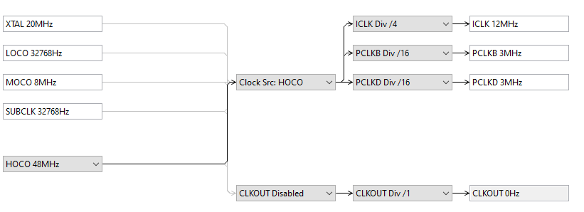
Changing clocks in this way reduced power consumption from 61.5 mA to approx.. 56.4 mA. Power saving is 5 mA which is about 8% of device original power consumption.
The next thing which I considered were sleep modes. There are several sleep modes but except the minimal mode all requires reconfiguring clocks before entering sleep. I can’t do this because my UART interface with Wi-Fi module is asynchronous and Wi-Fi module can send some status change messages at random time (including time when MCU is sleeping). When module send message at the same time when MCU is sleeping I will lose it because UART would be clocked by different clocks at sleep time. Maybe there is some workaround for this, but I decided to do not spend further time with it. So, I did not use any special mode. But I found that FreeRTOS port provided as part of e2 studio already enables basic sleep mode in idle task, so at least basic sleep mode is deployed (by default).
Optimization #3: Debugger MCU
After checking datasheet and schematics, I found that it is possible to cut-off power to the debug MCU. There is cut trace. I shorted one additional pullup for prevent back powering debugger MCU from GPIO. The problematic is that after cut-off I was unable to flash new program to the device. So I was soldering jumper back and then desoldering it, and then soldering when needed to flash and desoldering again, and then soldering and then desoldering, ….
It was sufficient but later I found better way for bypassing debugger MCU without need to solder/desolder. I will describe it as optimization #6 later.
Optimization #4: Power LDO
Onboard LDO used for converting 5V to 3.3V is Renesas ISL80102. It support high currents but is very inefficient. First issue is that efficiency of dropout regulator is low by design but there is also other parameter – quiescent current and this is current consumed by regulator itself. At light load it is 7.5 mA in case of this regulator! Note that there are on the market available regulators with Iq in range of uA.
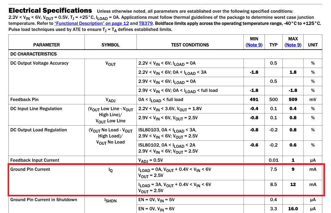
So, I decided to go alternative way. I was checking all regulators which I have home and decided to use my MAX16935 DC/DC module. It has best properties in comparison with all other regulators which I have. I desoldered LEDs from my module. In datasheet this regulator has mentioned quiescent current as about 40 uA (0.040 mA) which is much more better than 7.5 mA.
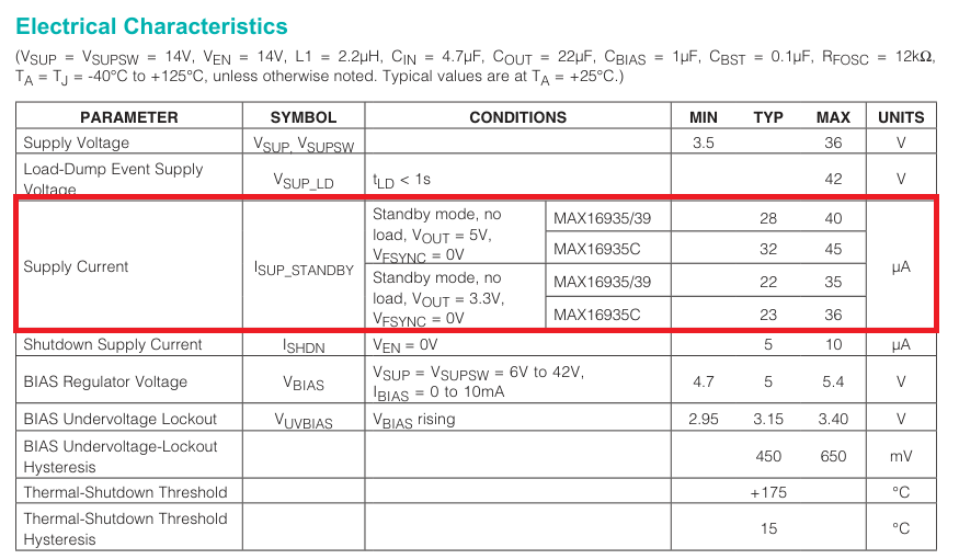
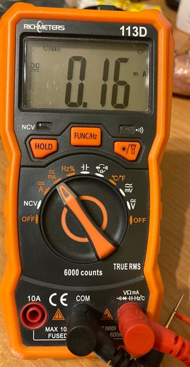
Note that this applies in specific conditions and also passives on my module consume some current. I measured current consumption without any load connected to it as 0.16 mA. It is not as good as 0.04 mA but still much better than several milliamps consumed by onboard LDO.
The remaining thing is that how to handle 5V voltage. After thinking I decided to bypass onboard regulator by providing regulated 3.3V to both 3.3V and 5V nets. This should bypass onboard LDO. I lose 5V branch but I do not need when powered from battery. Only need for 5V is when used with USB connected (only when flashing and debugging firmware).
Optimization #5: Battery Change
In previous optimization I changed regulator to regulator which withstand higher voltages (up to 36V). original onboard regulator withstands only 6V. Consequence is that now I can connect more batteries in serie to the regulator input and increase capacity in this way. At my second attempt I used 6xAA instead of 3xAA.
Optimization #6: Changing power cut-off to hold-in-reset
In optimizations 1 and 3 I cut of power to peripherals. But this had several side effects like need for soldering/desoldering shunts when using debugger. Similarly connecting transistor to cut-off power from Wi-Fi module significantly complicated connection because I need to add breadboard with transistor, route wires to both module and MCU board and interconnect remaining signals using wires.
So, I decided to change approach and instead of cutting power I decided to hold chips in reset. Idea is that they will have some static power consumption but in reset state digital logic inside chip is mostly suppressed and I guessed it will not be significant. I did it and power consumption did not grow significantly but design simplified significantly. It also simplified firmware little because I was not needed to set PMOD GPIOs to Hi-Z anymore and similarly debugging was easier because holding debugger MCU in reset is done by jumper.
Result
At the end I had design which continuously consume about 21.5 mA when Wi-Fi module is inactive (held in reset) and once per hour for several seconds it grows to 65 mA when Wi-Fi module is active.
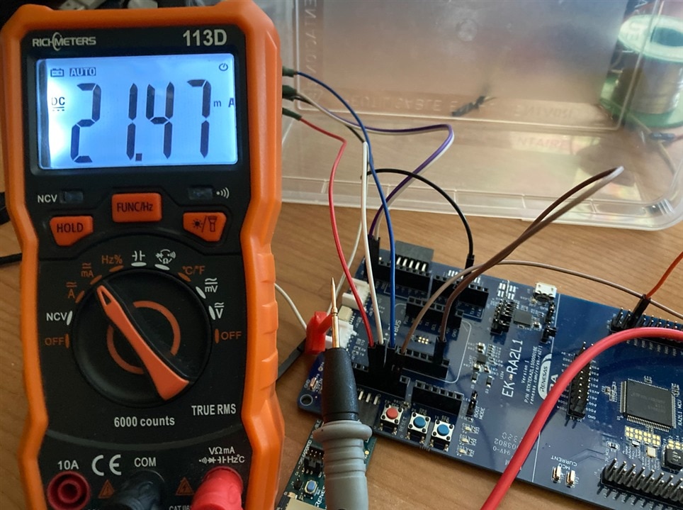
But 21.5 mA is power consumption on 3.3V net after voltage regulator. Because it is DC/DC regulator current drawn from source (battery) is lower because input voltage is higher than output. Theoretically because battery voltage 9V is about 3× higher than output voltage 3.3V we should see 1/3 of output current. But efficiency of regulator is not 100%, so in real power consumption is higher. Especially because our currents are low, and DC/DC stepdown converters are less efficient on these light loads.
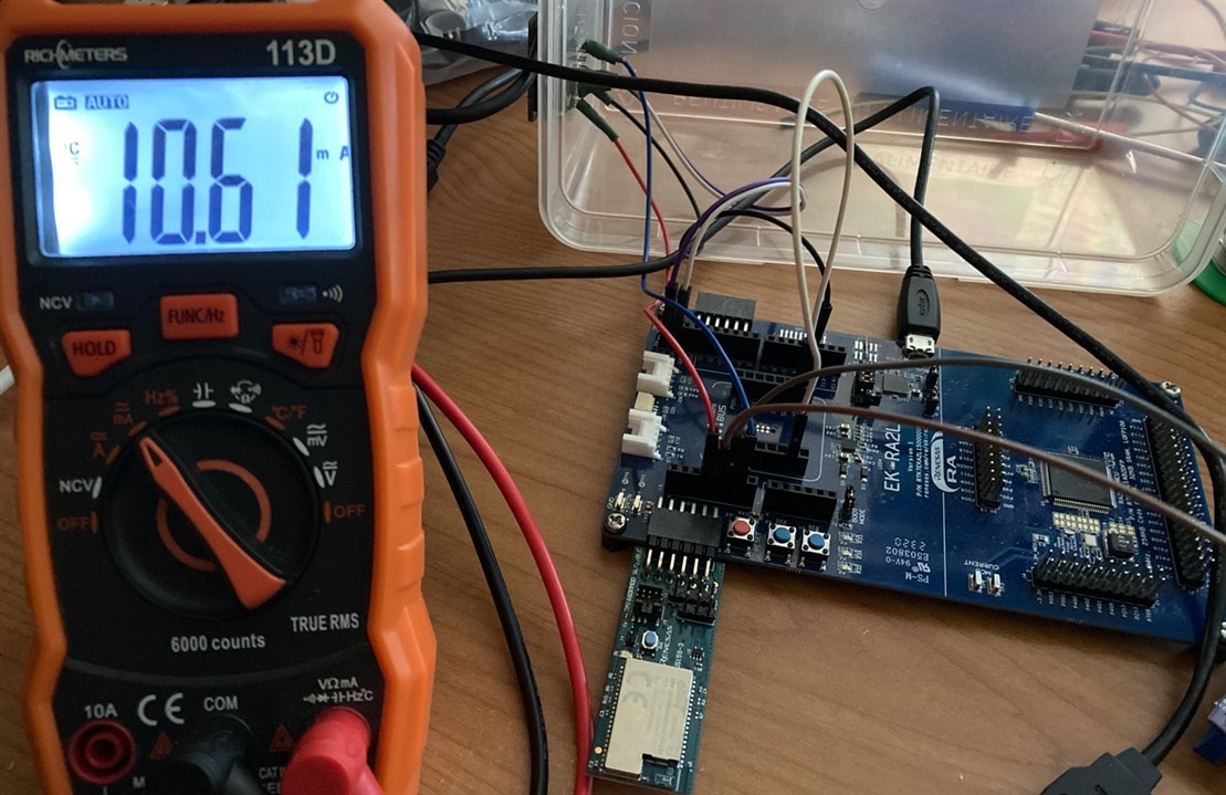
Finally, device draw 10.61 mA from battery which is much better than original 61.5 mA. It is not ideal and there is still space for optimizations in idle but all further optimizations which I took in account was very advanced and very hard to implement by deadline.
Summary
In this blog you have seen techniques which I used for reducing power consumption of my device and improving battery life of my device. In next blog I will show data from the sensor when running outside.
Time is running out and competition deadline is very near. I have already completed all my experiments, but I am busy with writing blog posts at this time.
Thank you for reading this blog. Have a nice day.
Next blog: Blog #8: ZMOD4510 Collected Data Analysis


-

dougw
-
Cancel
-
Vote Up
0
Vote Down
-
-
Sign in to reply
-
More
-
Cancel
Comment-

dougw
-
Cancel
-
Vote Up
0
Vote Down
-
-
Sign in to reply
-
More
-
Cancel
Children