
Welcome to the Analog Devices page on element14. Here you can find things such as our latest news, training videos, and product details. Additionally, you can engage with us in our forums.

by Rafael Marengo
We discussed how mobile robots navigate their environments through a variety of sensor types to collect data about the real world in the previous blog. However, we didn't explore how this data is communicated within the robot to translate perception into actions, such as movement.
Mobile robots consist of various technologies that must communicate with each other quickly and reliably to transmit critical messages for navigation and performing tasks, whether it's an Autonomous Mobile Robot (AMR) or an Automated Guided Vehicle (AGV). For a refresher on the differences between these types of robots, you can refer to this this blog in the series. Let’s consider the architecture of an AMR as shown:

Figure 1. AMR Communication Overview
There are several components that make up any mobile robot (such as wheel drive & encoder systems, vision inputs, inertial measurement unit (IMU) data, and battery management systems), and all of them need to communicate, usually with a main controller or main compute unit or sometimes to decentralized units that control specific functions of the robot, which can be done to reduce the overhead on a main controller and also aid in time critical applications such as perception of its environment and actuator control. There are many communication methods that live within the operation of a typical mobile robot, and each type of protocol has their pros and cons for use. In the above example there are potentially 7 different communication methods employed within the one mobile robot: GMSL, UART, CAN, Ethernet, RS-485, SPI, RS-422. While this blog focuses on wired communication protocols, it is important to note that mobile robots typically require wireless communication as well. Wireless communication is essential for enabling mobile robots to interact with a base station and collaborate with other robots, ensuring seamless coordination and operation in dynamic environments.
Here is a quick comparison of a selection of technologies comparing their speed and latency.

As it can be seen in table 1, the parameters for the highlighted technologies vary in speed and latency and the appropriate technology needs to be chosen according to the need and the design itself and will most likely include a combination of different technologies. Operations in mobile robots typically demand near real-time speeds to function effectively. This is crucial for tasks such as obstacle avoidance, navigation, and interaction with dynamic environments, where even slight delays can impact performance and safety. The key parameters that need to be taken into consideration for communication are performance, reliability, and scalability.
An AMR needs to be able to navigate while perceiving its surroundings to execute tasks in an efficient way, and a simple flow diagram can describe how it acts:

Both the perception and the action parts play important roles, the environment needs to be perceived in order for actions to be taken and this data is usually acquired with RGB cameras, depth cameras, Lidar sensors and radar or a combination but transferring all this data to a processing unit needs a robust link with enough bandwidth and in the case of industrial robots, reliability against interferences. That critical work can be executed by protocols such as GMSL.
Gigabit Multimedia Serial Link
There is a new protocol entering the mobile robotics scene, GMSL. The protocol can transfer up to 6 Gbps of advanced driver assistance systems (ADAS) sensor data over a coax cable while simultaneously transferring power and control data over a reverse channel. It is a highly configurable serializer deserializer (SERDES) interconnect solution which supports sensor data aggregation (Video, LiDAR, Radar, etc.), video splitting, low latency and low bit error, and Power over Coax (PoC)
The topology for a GMSL application consists of the sensor, a serializer, a cable, and a deserializer on the system on chip (SoC) side.

This simplifies the mobile robot design and makes it more robust since GMSL was designed with transferring this type of data and was optimized to ensure high bandwidth, low latency transmission of data.
The synergy between Industrial Ethernet, GMSL, and wireless communication technologies is driving the next generation of mobile robotics. These technologies provide the robust, high-speed, and flexible communication necessary for mobile robots to operate autonomously and efficiently in various environments. As innovations continue to emerge, the capabilities of mobile robots will expand, revolutionizing industries and transforming our daily lives. To learn more, visit analog.com/mobile-robotics.
WIRED COMMUNICATION
MAX96717R-AAK-EVK# Evaluation Kit
EVAL-ADIN1110EBZ Eval Kit ADIN1110BCPZ ADIN1110CCPZ
DEMO-ADIN1100D2Z Evaluation Kit EVAL-SPOE-KIT-AZ Evaluation Kit ADIN1100BCPZ ADIN1100CCPZ EVAL-ADIN1100EBZ
EVAL-ADIN1200FMCZ Evaluation Kit EVAL-10BT1L-MCS-BZ Evaluation Kit EVAL-10BT1L-MCS-AZ Evaluation Kit ADIN1200BCP32Z
EVAL-ADIN1300FMCZ Evaluation Kit EVAL-CN0506-FMCZ ADIN1300CCPZ ADIN1300BCPZ
WIRELESS COMMUNICATION
The MAX32630FTHR chip comes with a very handy feature. You can set the logic level for any GPIO in software. You can define your logic level either at 3V3 level (default) or at 1V8 logic level with the following commands: useVDDIOH(pin_no) for 3V3 and useVDDIO(pin_no) for 1v8.

Little did I realise that I would find a useful application for this feature so soon.
Over the weekend I decided to set up my Arduino Q board. This did not go smoothly. I found that my board would not always boot up correctly (see video). So, when I did get access to the board I decided to do a full system upgrade. This then locked me out the board, so to speak, on reboot as the HDMI stopped working. A quick SSH into the board confirmed that all was fine but it did prompt me to look at whether you get access to a debug UART port, like with a Rasberry Pi board for example.

The official Arduino Q users manual webpage confirmed that you do have access to a debug UART via the JCTL header pins. The gotcha is that this is 1V8 logic. Of course you can simply use a logic level shifter to handle this, as the JCTL connector includes a handy +1V8 VOUT pin. But this is all rather messy, in my opinion.
To solve this, I simply grabbed my MAX32630FTHR feather board and flashed it with the standard Arduino passthrough example with a couple of code amendments.

I needed to use "Serial2" at 1V8 logic, which is provided on pins P3_0 and P3_1. I decided to also start with 115200 baud rate, but as I'm not constrained by the speed of the logic level shifter, I could go push this higher if needs be.
/*
  SerialPassthrough sketch

   created 23 May 2016
  by Erik Nyquist

  https://docs.arduino.cc/built-in-examples/communication/SerialPassthrough/
*/

void setup() {
  Serial.begin(115200);

  // set the 1v8 logic for P3_0 and P3_1
  useVDDIO(P3_0);
  useVDDIO(P3_1);

  Serial2.begin(115200);
}

void loop() {
  if (Serial.available()) {        // If anything comes in Serial (USB),
    Serial2.write(Serial.read());  // read it and send it out Serial1 (pins 0 & 1)
  }

  if (Serial2.available()) {       // If anything comes in Serial1 (pins 0 & 1)
    Serial.write(Serial2.read());  // read it and send it out Serial (USB)
  }
}
And that's it. You then connect the two boards with 3 wires (for RXD, TXD, and GND):

And here's the result. It works a charm.
What makes this really handy is that I can now search in real time for keywords etc. The MAX32630FTHR ARM Cortex M4 is well suited for this.
by Sarvesh Pimpalkar
Previously we discussed the importance that inertial measurement units (IMUs) play in localization for autonomous mobile robots (AMRs) in a Localization: The Key to Truly Autonomous Mobile Robots - element14 Community. Today we will elaborate on how navigation relies on a fusion of sensor technologies working together to allow AMRs true freedom within dynamically changing environments.
So how do mobile robots learn to get around? As kids we are all thought to “stop, look and listen” before crossing a road, but does this same concept apply to robots. As humans we rely on our eyes and ears to help us “navigate” our environment, robots on the other hand use sensors to provide an awareness of their surroundings.
AMRs use Simultaneous Localization and Mapping (SLAM) techniques to navigate. The process involves the AMR being driven around the facility and scanning its environment. These scans are combined and generate a complete map of the area. AMRs utilize an array of sensors and algorithms for localization and navigation. Sensor technology such as industrial vision time-of-flight cameras, radar and lidar are the “eyes” of an AMR, combined with data from IMUs and wheel odometry (position encoders).
However, no single sensor is perfect. The true power lies in the diverse sensor types working together to produce effortless navigation in dynamically changing environments.
Each sensor has strengths and weaknesses that are balanced out by having more than one sensor type being relied on for navigation purposes. Let’s consider how multiple sensors can enhance the overall AMR performance.
Environmental Factors while Navigating
Lidar sensors can be sensitive to various environmental factors, such as ambient light, dust, fog, and rain. These factors can degrade the quality of the sensor data and, in turn, affect the performance of the SLAM algorithm. Similarly, other sensor modalities can be affected by reflective surfaces, dynamic moving objects (other AMRs or workers) thus further confusing SLAM. The table below summarizes how environment affects different sensors modalities.

Table 1: Comparison table of sensor modalities
While IMUs and wheel odometry are not affected by visual elements within the working environment, the use of this sensor data in conjunction with visual data means the AMR can operate better in any scenario encountered. Let’s consider the challenge of navigating on a sloping floor surface.
Navigating on a Slope
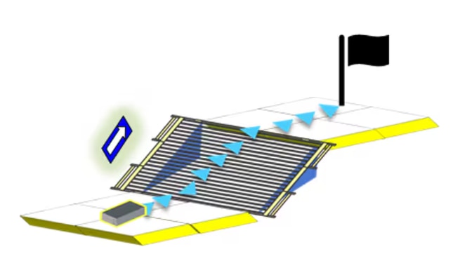
While maneuvering on a slope, traditional SLAM algorithms encounter challenges when relying on lidar, as the 2D point data does not show gradient information. Consequently, slopes are misconstrued as walls or obstacles, leading to higher cost maps. As a result, conventional SLAM approaches with 2D systems become ineffective on slopes. IMUs help to solve this challenge by extracting gradient information to effectively negotiate navigating on a slope.
How does the sensor data get combined?
In a typical ROS (Robot Operating System), vision sensors along with IMU and wheel odometry are combined through a process called sensor fusion. A widely used opensource ROS package is robot_locatlizaton1 which utilizes EKF (Extended Kalman filtering) algorithms at its core. By fusing data from diverse sensors such as lidar, cameras, IMUs, and wheel encoders, EKF helps in better estimating and understanding of the robot's state and its environment. Through recursive estimation, EKF refines the robot's position, orientation, and velocity while simultaneously creating and updating a comprehensive map of the surroundings. This fusion of sensor data enables mobile robots to overcome individual sensor limitations and navigate complex terrains with greater precision and reliability. By leveraging techniques like EKF help in collective insights of sensors, deriving meaningful sensor fusion of various sensor modalities allowing mobile robots to effectively perceive and interact with their environment and help navigate AMRs autonomously.
A future blog in this series will cover the Robot Operating System in more detail. However, the focus of this blog is to leave you confident that sensor fusion offers increased reliability, increases the quality of data, while providing greater safety for objects and people within the environment as AMRs aren’t relying on a single means to navigate. To learn more visit analog.com/mobile-robotics.
Reference / Resources:
1 https://docs.ros.org/en/melodic/api/robot_localization/html/index.html
ADTF3175 1 MegaPixel Time-of-Flight Module
ADTF3175BMLZ ANALOG DEVICES, Imaging Module, 1024 x 1024 Active Pixel, 3.5µm x 3.5µm | Farnell® Ireland
EVAL-ADTF3175 Time-of-Flight Evaluation Kit
EVAL-ADTF3175D-NXZ ANALOG DEVICES, Evaluation Board, ADTF3175, ADSD3100 | Farnell® Ireland
by Sarvesh Pimpalkar
In our previous blog Finding the Right Fit for your Industrial Automation Need - AGVs or AMRs we explored the key differences between Automated Guided Vehicles (AGVs) and Autonomous Mobile Robots (AMRs). One major takeaway was that AMRs hold a clear advantage when navigating dynamic environments, thanks to their superior sensing capabilities and advanced computing power.
But why exactly do these features make such a difference?
In this next series, we will dive deeper into the technology behind AMRs and uncover how their advanced perception and decision-making enable them to adapt, respond, and thrive in complex, ever-changing industrial settings. Stay tuned as we break down the reasons AMRs are redefining flexibility and efficiency in automation.
Localization is the process of determining where a robot is located within its environment. For mobile robots, the ability to map its surroundings and identify its position relative to that map are key. With greater localization awareness, tasks can be performed faster and more efficiently, as the majority of a mobile robot’s tasks involve moving from one location to another. It is this freedom of movement that gives AMRs independence within a factory, but how does it work?
Introduction to Inertial Measurement Units (IMUs)
Inertial Measurement Units (IMUs) provide crucial motion data for precise robot positioning. Integrated accelerometers measure acceleration with respect to the earth’s gravitational field, gyroscopes measure the rate of rotation providing angular velocity, and magnetometers support accurate orientation estimation in challenging environments. By integrating all three of these advanced sensing technologies, IMUs enable robots to precisely determine their orientation, position, and movement. Let’s consider the challenges for localization and how IMUs overcome these.
Dead Reckoning: A navigation technique to estimate current position based on a previously known position. By constantly providing data on position, orientation, and speed over elapsed time, IMUs enable precise estimation, contributing to reliable navigation for AMRs.
Robustness: Environmental factors can have a significant impact on sensor performance. Lidar sensors, for instance, may exhibit sensitivity to ambient light, dust, fog, and rain, resulting in decreased sensor data quality and potential disruptions in performance. Other sensor modalities, such as cameras, may encounter challenges from reflective surfaces and dynamic obstacles like other AMRs or workers. In contrast, IMUs demonstrate robustness across diverse conditions, including environments with electromagnetic interference, enabling them to operate effectively both indoors and outdoors. This adaptability makes IMUs an optimal choice for mobile robots, ensuring consistent performance in the face of environmental complexities.
Enhanced Reliability: IMUs stand out by providing high-fidelity positional output of up to 4kHz raw data. Other perception sensors are typically limited to update rates of ~10Hz to 30Hz. This increased update rate enhances reliability of IMU performance, especially in dynamic environments, enabling AMRs to estimate their position quickly and accurately in the short time between other measurements.

IMUs Versus Visual Odometry
You might be wondering, with the advancement in vision systems, why is the IMU still playing such a pivotal role in mobile robotics? Here’s why:
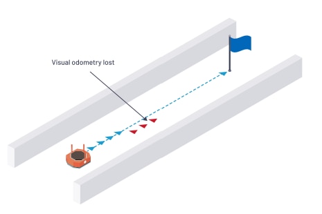
SLAM (Simultaneous Localization And Mapping) algorithms match observed sensor data with stored data to localize within the map. But what happens when observed sensor data is limited, for example in a long corridor with straight walls of uniform color, texture, or reflectivity? SLAM algorithms can struggle to localize precisely in such environments, and the AMR is likely to lose its position quickly due to a lack of distinctive features.
IMUs act as a valuable guidance system by providing heading and orientation information in feature-sparse environments such as corridors. They provide high short-term accuracy and immediate measurements between vision sensor measurements. IMUs have lower computational needs than visual odometry, enhancing redundancy and further endorsing them for AMR operations.
While IMUs offer many benefits over other sensors, they can also be prone to drift. In situations where the environment is constantly changing, it may be advantageous for AMR operations to rely on multiple sensor inputs. This allows each sensor to overcome the limitations of the others for greater success. The next blog of the series will explore how this sensor fusion works and the combined benefit it brings to robotics.
Factories of the future may be purpose built and optimized for AMRs to operate in, but adapting these robots to existing warehouses and factories presents challenges. Learn more about how ADI’s IMU technology can be utilized in mobile robotics at analog.com/mobile-robotics.
ADIS16500AMLZ ANALOG DEVICES, MEMS Module, Accelerometer, Gyroscope | Farnell® Ireland
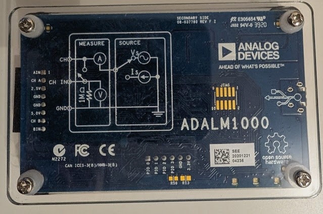
During my search for a low cost electronics learning module, I came accross the ADALM1K which has interesting features for the price point (approx. 70$). It incorporates a source measure unit (SMU), an oscilloscope and a function generator. On top of that the hardware and software is open-source which is a learning experience in itself to undestand how the kit works.
My goal was first to test how the kit works overall. Once I had some confidence in its usage functions, I dived deeper into its evaluation / application software to look for automation oppurtinites with Python, where one could automate custom workflows for measurement and learning purposes.
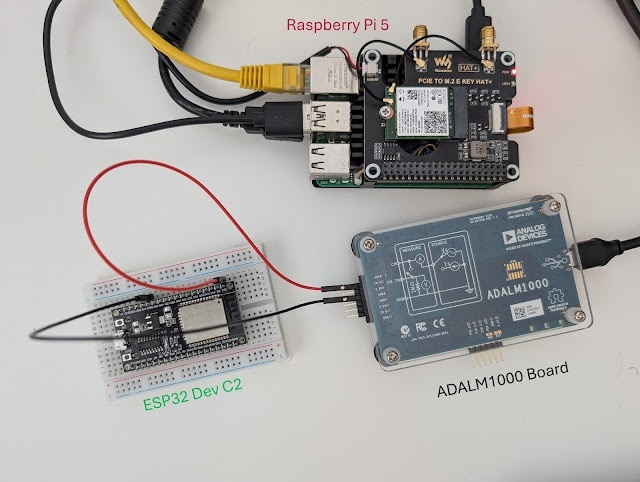
I was able to integrate the ADALM1K with my Raspberry Pi setup and automate its functionality using the provided libsmu/pysmu Python package from Analog. I ended up creating a small Python library (pytest-analog) around libsmu so I could write some automated tested for my projects usning the ADALM1K.
As an example, I created automated test cases via Python to measure the power consumption of a DUT (ESP32 Dev board). This could be extended to create more complex test cases for your system under test using very low cost equipment such as the ADALM1K
The main hardware sepcs are as follows:
 |
| ADALM1K Block diagram per SMU Channel (wiki.analog.com) |
As per the above the diagram, an analog channel on the ADALM1K combines a function generator and an oscilliscope instrument on the same pin. In Rev F of the board, the analog ouput and input functions could be seperated with the two provided addiotnal split pins such that the oscillscope function is brought out along with 1 MΩ from the function generator function. Therefore, each analog channel could be configured to one of the following options:
If you would like to learn more about the ADALM1K hardware and its design, the following resources are good to read through:
 |
| ADALM1000 Board Upside View |
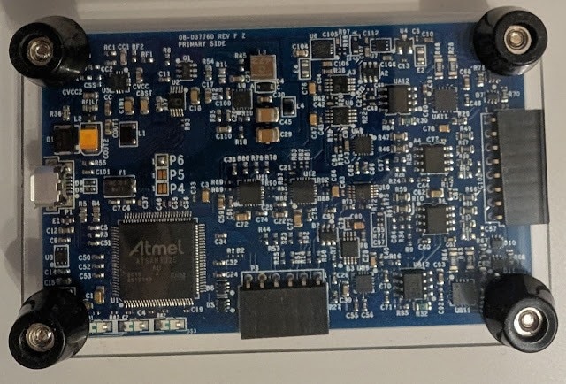 |
| ADALM1000 Board Underside View |
The software landscape of the ADALM1K comprises the device firmware and the host software which can run on different platforms (Winodws / Linx / OS-X).
The ADALM1K firmware runs on an Atmel based microcontroller. The host software includes a C++ library (libsmu) containing the abstractions for streaming data to and from ADALM1K via USB. In addition, the Pixelpulse 2 and ALICE GUI-based tools are available to control the ADALM1K and make measurements with it.
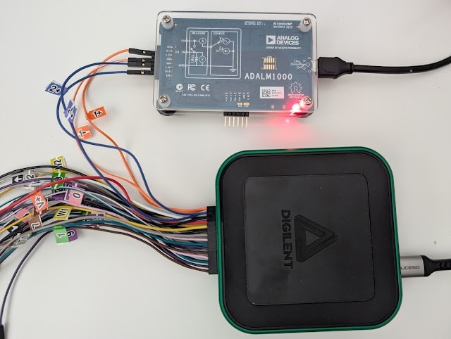
In order to test the opertion of the ADALM1K via the provided GUI software Pixelpulse 2 and ALICE, I did some basic checks to test the ADALM1K analog and digital inputs/outptus via my Analog Discovery 3 (another great electronics learning tool). In these tests, I connected the two instruments to my PC and started their host softwares simultaneously to feed inputs and read outputs.
Test 1: Checking analog outputs of the ADALM1K via the Analog Discovery scope channels:
As shown in the image below, I connected the ADALM1K source channels A, B to the Analog Discovery scope channels 1, 2. Then using ALICE software I configured an output voltage on channels A, B and then read measured voltages on the scope channels via the WaveForms software of Analog Discovery 3. I configured channels A, B to output 3.6, 1.2 V. On the Analog Discovery, I read approximately similar values on channels 1, 2. There is a slight 200 mV deviations which also seem to occur when I set the ADALM1K to ouput 0 V. Therfore, the ADALM1K requires some calibration before doing any real testing.

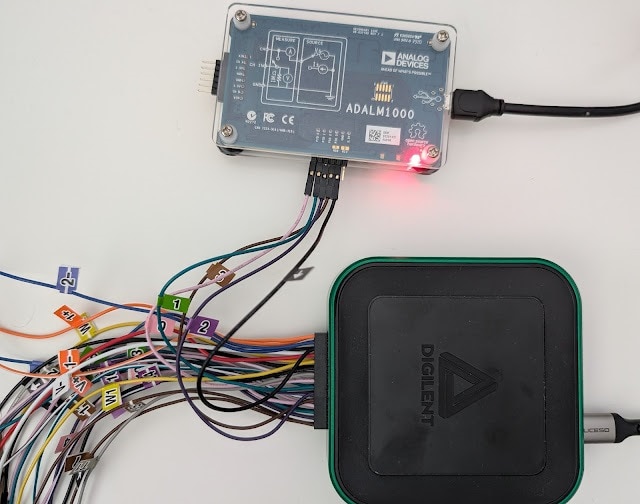
Test 2: Checking GPIOs state of the ADALM1K via the Analog Discovery digital channels:
In this test, I connected the ADALM1K GPIO pins (0-3) to the Analog Discovery Digital IOs (0-3). Using ALICE software, I have set the ADALM1K GPIOs to a defined high / low state and then checked if the same state is read on the Analog Discovery side using its Static IO instrument in the WaveForms software. I was able to confirm the GPIOs state (high for pins 0,1 and low for pins 2,3
)


After integrating the ADALM1K with my Raspberry Pi setup and getting familiar with the libsmu / pysmu libraries, I decided to create a small python library (wrapper class) to ease the control of the instrument functions and also create pytest-fixtures for setting up / tear down of the instrument in an automated testing environment. The library is named pytest-analog and it also support the automation of the Analog Discovery instrument from Digilent.
To demonstrate the usage of ADALM1K with pytest-analog in automated testing context, I created a small python test case where the ADALM1K would measure the power consumption of an ESP32 microcontroller running different sketches.
Given the instrument source and measure capabilites, it can power the ESP32 with a given voltage and measure drawn current simultaneously.
The steps to create an automated test with the ADALM1K via pytest-analog are listed below:
[pytest]
# pytest options
addopts = -v --capture=tee-sys

# Filtering Warnings
filterwarnings =
    ignore::DeprecationWarning

# Logging Options
log_cli=true
log_level=INFO
log_format = %(asctime)s %(levelname)s %(message)s
log_date_format = %Y-%m-%d %H:%M:%S

# ADALM1000 Fixtures Options
# Voltage Source
adalm1k_ch_a_voltage = 3.30
adalm1k_ch_b_voltage = 0.00 import numpy as np
import pytest
import time
import math
import logging
import matplotlib.pyplot as plt
from pytest_analog import ADALM1KWrapper, AnalogChannel
from datetime import datetime
def test_esp32_current_consumption(
adalm1k_voltage_source: ADALM1KWrapper
) -> None:
# 2000 samples collected at base rate 100 kHz with averaging every 1000 samples -> 20 seconds
MEASUREMENTS_COUNT = int(2000)
# Do some averaging over collected data
AVERAGE_RATE = int(1e3) # average every 1 / AVERAGE_RATE, Default sampling rate of ADALM1K is 100 kHz
samples = []
ch_a_avg_voltage = []
ch_a_avg_current = []
# Read incoming samples in a blocking fashion (timeout = -1)
for _ in range(MEASUREMENTS_COUNT):
samples.append(adalm1k_voltage_source.read_all(AVERAGE_RATE, -1))
# Average captured readings
for idx in range(MEASUREMENTS_COUNT):
# voltages in V
ch_a_voltage = [sample[0][0] for sample in samples[idx]]
# currents in mA
ch_a_current = [sample[0][1] * 1000 for sample in samples[idx]]
ch_a_avg_voltage.append(np.mean(ch_a_voltage))
ch_a_avg_current.append(np.mean(ch_a_current))
logging.info(f"Average current consumption: channel A: {np.mean(ch_a_avg_current):.3f} mA")
logging.info(f"Max current consumption: channel A: {np.max(ch_a_avg_current):.3f} mA")
# plot current profile
t = np.arange(0, MEASUREMENTS_COUNT) / (100e3 / AVERAGE_RATE) # Default sampling rate is 100 kHz
fig, ax = plt.subplots()
fig.suptitle(f"ESP32 Blinky current consumption", wrap=True)
fig.supxlabel("Time (s)")
ax.plot(t, ch_a_avg_current, color='red')
ax.set(ylabel= "CH_A I(mA)")
ax.margins()
ax.set_xlim([0, math.ceil(np.max(t))])
ax.grid(True, which='both')
ax.minorticks_on()
plt.savefig(f"I_consumption_esp32_blinky_{time.strftime(datetime.now().strftime('%H%M'))}.png")
 |
| Current consumption profile for ESP32 blinking an LED every 2 seconds |
 |
| Current consumption profile for ESP32 going into deep sleep mode for 5 seconds then waking up shortly |
After the test execution, a graph is generated with the measured current consumption profile during the test. The graphs above are for two different sketches running on the ESP32.
The first one is a basic blinky sketch where one could certainly see an increase in current draw when the LED is on. The duration of those peaks match closely with the LED-On period as expected.
The second sketch showcases the ESP32 deep sleep mode for extreme power saving applications, where the device is consuming a couple of miliamps during sleep mode and then waking up shortly every 5 seconds.
IMPORTANT: The above results can be inaccurate and require verification with a professional equipment to compare how good the ADALM1K is in capturing power characterstics of a given DUT.


.png-100x100x2.png?sv=2016-05-31&sr=b&sig=%2FGbIOj3u58gIWVutzm12eJRyFzb%2F4pNyYYEtPV68dWo%3D&se=2026-06-15T23%3A59%3A59Z&sp=r&_=MSQhnf5EMGSMX+OYc3S0yA==)


