


Application Note
EMI Filter Design for Non-Isolated DC/DC Converters
ANS018 by Timur Uludag
1. INTRODUCTION
Today, many industrial applications run with input voltage levels such as 5VDC or lower, as shown in Figure 1. The power distribution system used to power such applications is often a DC bus voltage of 24VDC. DC/DC power modules are commonly chosen to handle the conversion of the higher DC bus voltage down to the lower voltage level.
A clear advantage that comes with the use of power modules is that very high efficiencies (often greater than 90%) can be realized. However, the switching behavior of these modules present additional design challenges. Constant switching during operation generates interference energy that can a negative impact on the components in the application. Therefore, developers should always check whether EMI filtering measures are required in their design when using DC/DC power modules.
Figure 1 shows the block diagram of a typical industrial environment application with a 24VDC bus. Non-isolated power modules are used to provide the operating voltage of all subsystems. This indicates the importance of DC/DC converters for industrial applications, since these existing subsystems must be supplied with different voltage levels. The converted voltages can be used to supply programmable logic controller systems or further peripheral interfaces for data acquisition, data transmission or human-machine interfaces such as industrial control panels. The DC/DC power module 171032401 is a fully integrated DC/DC converter including the switching regulator IC with integrated MOSFETs, compensation and a shielded inductor in a single housing. For physical reasons, the switching processes of the MOSFETs cause EMC interference in every DC/DC converter, whether discrete or fully integrated as in the power module. Based on the switching frequency, this interference can occur in the EMC measurement, e.g. as conducted harmonic interference amplitudes. Therefore, a fundamental understanding of the EMI basics is essential for the topic of EMI filter for Non-Isolated DC/DC Converters. Chapter 2 and 3 will provide the basics about the types of emissions and the noise modes here.
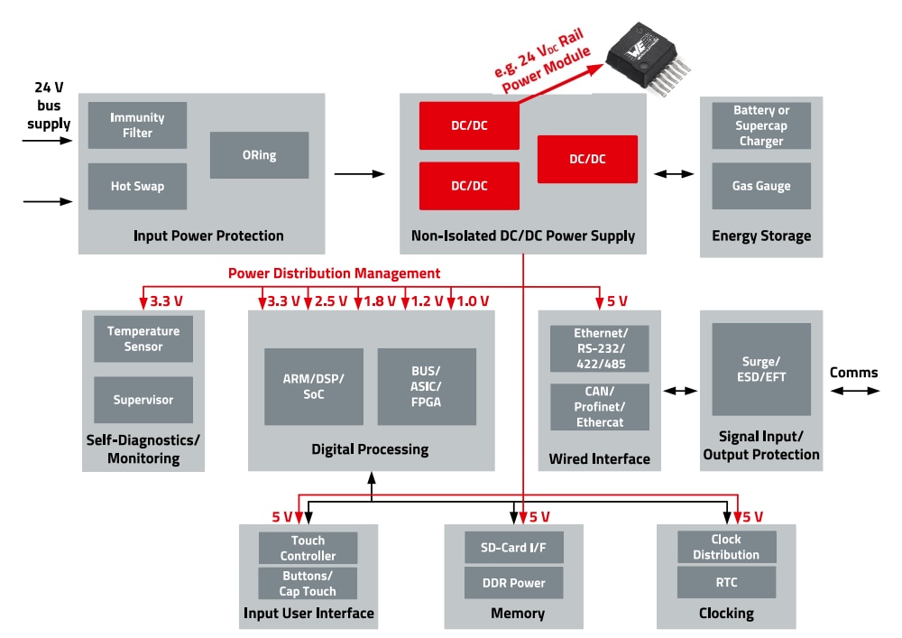
Figure 1: Typical industrial application environment.
2. TYPES OF EMI EMISSIONS
2.1 Conducted EMI
Conducted emissions are interferences that propagate via the connecting lines of the device. This type of interference voltage is usually specified logarithmically as dBµV and is an alternating voltage.
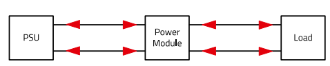
Figure 2: Block diagram of conducted EMI.
The arrows in Figure 2 symbolize disturbances that flow in different directions from different systems and can therefore be both sources and sinks. In case of power modules, the IEC 55032 / CISPR32 standard "Electromagnetic compatibility of multimedia equipment - Emission Requirements " (derived from IEC 55022 / CISPR22 and CISPR13) is used as a reference for the interference voltage limit values. This standard is used in the field of information technology. It contains the limits for the interference voltage in the frequency range from 150 kHz to 30 MHz. Two classes are defined regarding the application area:
- Class A: For use in industrial environment.
- Class B: For use in the immediate vicinity of residential, business and commercial areas.
The noise levels are divided into Max Peak, Quasi-peak and Average. The Max Peak only indicates the peak value of the interference level. The quasi-peak value evaluates the “modulation frequency” and intensity, i.e. amplitude of a signal. The more frequent the signal appears in its periodicity and the "louder" it is, the higher the quasi-peak value. This is used to evaluate pulsed signals with a low repetition rate. Figure 3 shows the CISPR32 limits for the Quasi-peak and average levels.
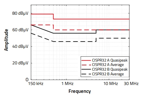
Figure 3: Limits for conducted EMI according to IEC 55032 / CISPR32.
2.2 Radiated EMI
In contrast to conducted interference emissions, radiated interference emissions are the transmission of interference from the interference source to the interference sink across the space and are measured in dBµV/m. Figure 4 represents the radiation of the power module and the connected load.
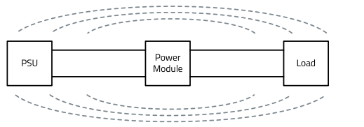
Figure 4: Schematic of radiated EMI.
The limits for the radiated interference field strength in the frequency range from 30MHz to 1GHz can also be taken from the CISPR32 standard. These are shown in Figure 5.
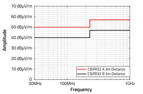
Figure 5: Limits of radiated EMI according to IEC 55032 / CISPR32.
3. NOISE MODES
3.1 Differential Mode
In the case of differential mode (DM) interference, the interference current flows in opposite directions in the forward and return conductors. These currents cause a corresponding voltage drop at the impedance of the interference sink. Figure 6 illustrates the DM current IDM between the interference source and the interference sink using a non-isolated MagI³C Power Module with a load connected at the output as an example.
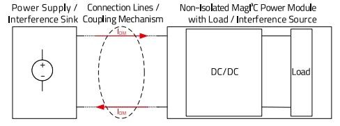
Figure 6: Differential mode interference.
3.2 Common Mode
The interference current ICM of common mode noise (CM) flows in the same direction in the forward and return conductors. In a symmetrical circuit design, these currents do not cause a voltage drop at the interference sink between the forward and return conductors. However, the interference voltage VCM can be measured against ground. In addition to the DM input current, a common-mode current is most frequently observed with isolated power modules. The common mode circuit is closed by the coupling capacitances between primary and secondary windings. To enable current flow in the same direction on the forward and return path, the stray capacitances to ground must be taken into account. Consideration of these stray capacitances is the only way for the noise circuit to be closed. This is shown in Figure 7 using an isolated MagI³C Power Module with a connected load as an example. The stray capacitances are symbolized as CP1 with connection to ground.
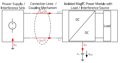
Figure 7: Common mode interference.
4. REDUCE INTERFERENCE THROUGH PASSIVE FILTERS
Passive filters are frequency dependent current and voltage dividers made of L, C and R components. These current and voltage dividers reduce spurious emissions from the power module at the interference sink. However, the filtering effect in real passive devices is limited because they always have parasitic elements. For example, above the resonant frequency, the capacitor increasingly behaves like an inductor and exhibits inductive phase behavior. This means that the phase shift gradually changes from -90° (capacitive) to +90° (inductive). The capacitor now acts as an inductive impedance, as the parasitic inductance dominates, and the impedance increases with increasing frequency.
Similarly, the capacitive influence increases with inductors above the resonant frequency. The phase shift gradually moves into the negative range and approaches -90° (capacitive behavior), whereby the progression is continuous and dependent on the frequency. In this range, the coil is more or less a capacitor, as the parasitic capacitance now has a stronger effect than the inductance. However, this does not mean that the components no longer have any filter effect from this point on. Instead, it means that from this frequency on, careful attention must be paid to the impedance of the component to determine the corresponding filter effect. But since this application note is about conducted interference in the frequency range up to max. 40MHz regarding DC-DC converters most passive components (inductors & capacitors) can be used for EMI suppression. The larger challenge with the circuits considered is to find a clean reference ground for the capacitor and to prevent "over coupling" of the filter. 1
1This application note focuses on passive filters for non-isolated MagI³C power modules and thus on filtering of DM interferences. For an understanding of the filtering of CM interferences as well as the passive filter design for isolated MagI³C power modules, at this point reference is made to the WE application note ANS022.
5. EMI FILTER DESIGN FOR NON-ISOLATED MAGI³C POWER MODULES
In order to effectively filter both conducted interference and radiated interference from the power module, a series impedance (choke) and a bypass impedance (capacitor) are added to the input circuit, resulting in a low-pass filter with an attenuation of 40 dB/decade.
Normally, the power module is operated with a necessary input capacitor, which must be considered in the filter configuration. The resulting filter design is generally referred to as a PI filter. Figure 8 shows the circuit diagram of the LC filter including the interference sink (LISN)2 and a non-isolated MagI³C power module shown as the interference source (constant current source). Here the complex impedance ZBP1 corresponds to the input capacitor, ZBP2 corresponds to the added bypass capacitor, ZL to the series inductance and ZV to the impedance of the interference sink.
2 Here only conducted emissions up to 30MHz are considered. Above 30 MHz the impedance concept of the LISN doesn’t work anymore because it is supposed to replicate the typical impedance of a household mains connection.
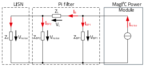
Figure 8: EMC model with the MagI³C power module as current source.
To simplify the model, the constant current source is converted into a constant voltage source, whereby the first bypass impedance ZBP1 (impedance of the input capacitor) is integrated into the voltage source. This can be done by considering the input capacitor as a very low impedance compared to the inductor impedance and the LISN impedance. This means that the input capacitor is the dominant part and defines the voltage by drawing the main current in this setup. This results in an LC filter due to the series impedance, ZL, and the second bypass impedance, ZBP2.
The resulting circuit diagram is shown in Figure 9.
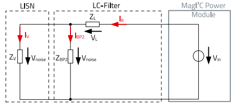
Figure 9: EMC model with the MagI³C module as voltage source.
Using the assumptions just discussed, the attenuation of an LC filter can be calculated as follows. The voltage VIN is the voltage that occurs when the power module is connected only with input capacitors to the LISN. Consequently, A1 corresponds to the measured amplitude of a power module without further filtering and A2 corresponds to the measured amplitude with an additional filter.
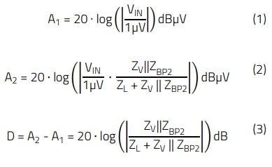
The difference between A2 and A1 is the damping D.
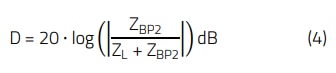
This formula can be simplified if the dominant parts of the circuit are considered. It can therefore be assumed that if a capacitor is used as ZBP2, this is the dominant part and the parallel circuit can be reduced to this. This results in the following formula:
This formula can be further simplified under the condition that ZL ≫ ZBP2. This is due to the fact that ZL is the dominant part for the current in this curcuit.
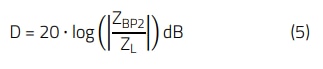
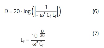
To determine the component values, this formula must be converted to use C and L values, see Figure 10.
When designing passive filters, it must be considered that the filter components are not ideal and have parasitic impedances as mentioned already. Furthermore, the components often show a derating with respect to voltage and/or current. For example, the capacitance of a capacitor, depending on its material and design, decreases with an increasing DC bias voltage, likewise an inductor has a lower inductance with a higher DC current and must not reach core saturation (Reference Guide: Trilogy of Magnetics).
6. INPUT EMI FILTER FOR MAGI³C POWER MODULES
From the previous chapters, the filter design was explained theoretically. For the practical implementation, however, the exact components recommended will have an important role to play in creating an effective filter. The online design tool Redexpert4 from Würth Elektronik is perfectly suited for this purpose, as it maps the impedance curves of all the filter components. Additionally, use its EMI Filter Designer to recommend values and plot the resulting response. Due to the frequency behavior of MLCCs as well as polymer capacitors, these capacitor types are very well suited to be filter capacitors. The WE-PD2 series of inductors offers excellent characteristics for the role of filter inductance. To support developers in circuit design, Würth Elektronik offers application-specific filter configurations for isolated and non-isolated power modules. Figure 10 shows an example of a filter circuit of a non-isolated MagI³C power module with variable output voltage using the TO-263EP package (VDRM).
The module requires additional, external input capacitance (C2 and C3) to optimize the input current ripple. This input capacitance should be placed as close as possible to the power module.
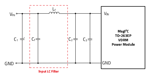
Figure 10: Input EMI filter for non-isolated MagI³C Power Modules.
This approach to input filter design is valid for the entire non-isolated MagI³C power module portfolio. Figure 11 and Figure 12 show the measured conducted emissions according to the IEC55032 / CISPR32 test setup with the evaluation board 178032401 of the 171032401 MagI³C module to provide real validation of the filter design.
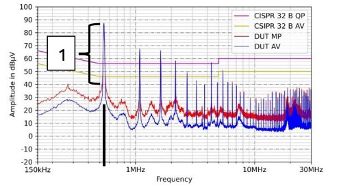
Figure 11: Measured conducted emission of MagI³C VDRM 171032401 without input filter.
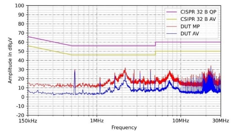
Figure 12: Measured conducted emission of MagI³C VDRM 171032401 with input filter.
The diagram shows that the limit values of the IEC55032 / CISPR32 are exceeded at the switching frequency of 500 kHz as well as with some of the following harmonics. Therefore, further attenuation D of more than 40 dB is needed see Figure 11 detail 1. With the equation we have already evaluated we can now calculate the needed value for the inductance L. To calculate the inductance L, we need an initial value for the capacitance C. Experiments have shown that 2 x 4.7 µF, i.e. twice the value of the input capacitance, is a sensible output value. This procedure has been verified experimentally and provides the most sensible output values. To have a more realistic value for the capacitor for the calculation we must take the DC bias effect into account (see REDEXPERT). The capacitance therefore will be set to 70% (6.8 µF) for the two capacitors 885012209048. D will be set to 55 dB to have here a good attenuation with enough margin (15 dB margin) to the limits:

After implementing the designed input LC filter with Lf = 6.8 µH (744774068) and Cf ≈ 10 µF (2x 885012209048), nearly 60 dB of attenuation could be achieved. The selected inductor has no derating in the current range under consideration. Furthermore, no limits are exceeded at any frequency within the spectrum range of 150 kHz to 30 MHz.
7. SUMMARY & CONCLUSION
In summary, using DC/DC power modules allows developers to profit from their high efficiency but does not remove the need for EMI filter design. Figure 13 shows a block diagram of the whole system, including the MagI³C filter concept, for overall EMC (radiated and conducted) compliance with the EMI IEC 55032 / CISPR32 standards, as well as to the surge and burst immunity standards IEC 61000-4-4 and IEC 61000-4-5. The emission reduction filter does not include protection against transient overvoltages, which must be added in practice. For this purpose, voltage-limiting components are added to the filter. A separate application note covers the details (ANS023).
For any application using a non-isolated DC/DC switching regulator, power module or not, EMI filtering must be considered. An improper EMI design leads to malfunctioning due to unwanted interferences of components in the application area. Also, other nearby electrical devices can be affected. Therefore, to reach EMI compliance it is mandatory to consider EMI filtering. This application note represents the best EMI counter measures, whether the non-isolated DC/DC converter is implemented discretely or as a compact package solution of a power module. Würth Elektronik offers comprehensive, competent technical support for all EMI filter designs as well as EMS protection designs including customer design-in support and layout reviews (MagI³C Service & Support).
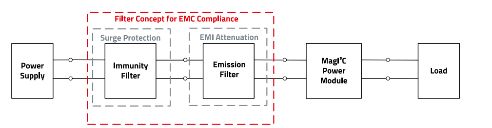
Figure 13: MagI³C filter concept for EMC compliance to IEC 55032 / CISPR32, IEC 61000-4-4 and IEC 61000-4-5.
IMPORTANT NOTICE
The Application Note is based on our knowledge and experience of typical requirements concerning these areas. It serves as general guidance and should not be construed as a commitment for the suitability for customer applications by Würth Elektronik eiSos GmbH & Co. KG. The information in the Application Note is subject to change without notice. This document and parts thereof must not be reproduced or copied without written permission, and contents thereof must not be imparted to a third party nor be used for any unauthorized purpose. Würth Elektronik eiSos GmbH & Co. KG and its subsidiaries and affiliates (WE) are not liable for application assistance of any kind. Customers may use WE’s assistance and product recommendations for their applications and design. The responsibility for the applicability and use of WE Products in a particular customer design is always solely within the authority of the customer. Due to this fact it is up to the customer to evaluate and investigate, where appropriate, and decide whether the device with the specific product characteristics described in the product specification is valid and suitable for the respective customer application or not. The technical specifications are stated in the current data sheet of the products. Therefore the customers shall use the data sheets and are cautioned to verify that data sheets are current. The current data sheets can be downloaded at www.we-online.com. Customers shall strictly observe any product-specific notes, cautions and warnings. WE reserves the right to make corrections, modifications, enhancements, improvements, and other changes to its products and services. WE DOES NOT WARRANT OR REPRESENT THAT ANY LICENSE, EITHER EXPRESS OR IMPLIED, IS GRANTED UNDER ANY PATENT RIGHT, COPYRIGHT, MASK WORK RIGHT, OR OTHER INTELLECTUAL PROPERTY RIGHT RELATING TO ANY COMBINATION, MACHINE, OR PROCESS IN WHICH WE PRODUCTS OR SERVICES ARE USED. INFORMATION PUBLISHED BY WE REGARDING THIRD-PARTY PRODUCTS OR SERVICES DOES NOT CONSTITUTE A LICENSE FROM WE TO USE SUCH PRODUCTS OR SERVICES OR A WARRANTY OR ENDORSEMENT THEREOF. WE products are not authorized for use in safety-critical applications, or where a failure of the product is reasonably expected to cause severe personal injury or death. Moreover, WE products are neither designed nor intended for use in areas such as military, aerospace, aviation, nuclear control, submarine, transportation (automotive control, train control, ship control), transportation signal, disaster prevention, medical, public information network etc. Customers shall inform WE about the intent of such usage before design-in stage. In certain customer applications requiring a very high level of safety and in which the malfunction or failure of an electronic component could endanger human life or health, customers must ensure that they have all necessary expertise in the safety and regulatory ramifications of their applications. Customers acknowledge and agree that they are solely responsible for all legal, regulatory and safety-related requirements concerning their products and any use of WE products in such safety-critical applications, notwithstanding any applicationsrelated information or support that may be provided by WE. CUSTOMERS SHALL INDEMNIFY WE AGAINST ANY DAMAGES ARISING OUT OF THE USE OF WE PRODUCTS IN SUCH SAFETYCRITICAL APPLICATION.
DIRECT LINK
ANS018 | EMI Filter Design for Non-Isolated DC/DC Converters
USEFUL LINKS:
Application Notes : https://we-online.com/en/support/knowledge/application-notes
Services: https://we-online.com/en/products/components/service
Contact : https://we-online.com/en/support/contact
CONTACT INFORMATION
Würth Elektronik eiSos GmbH & Co. KG
Max-Eyth-Str. 1, 74638 Waldenburg, Germany
Tel.: +49 (0) 7942 / 945 – 0
Email: appnotes@we-online.de
