element14 Community
element14 Community
    Register Log In
  • Site
  • Search
  • Log In Register
  • Members
    Members
    • Benefits of Membership
    • Achievement Levels
    • Members Area
    • Personal Blogs
    • Feedback and Support
    • What's New on element14
  • Learn
    Learn
    • Learning Center
    • eBooks
    • STEM Academy
    • Webinars, Training and Events
    • Learning Groups
  • Technologies
    Technologies
    • 3D Printing
    • FPGA
    • Industrial Automation
    • Internet of Things
    • Power & Energy
    • Sensors
    • Technology Groups
  • Challenges & Projects
    Challenges & Projects
    • Design Challenges
    • element14 presents
    • Project14
    • Arduino Projects
    • Raspberry Pi Projects
    • Project Groups
  • Products
    Products
    • Arduino
    • Dev Tools
    • Manufacturers
    • Raspberry Pi
    • RoadTests & Reviews
    • Avnet Boards Community
    • Product Groups
  • Store
    Store
    • Visit Your Store
    • Choose Another Store
      • Europe
      •  Austria (German)
      •  Belgium (Dutch, French)
      •  Bulgaria (Bulgarian)
      •  Czech Republic (Czech)
      •  Denmark (Danish)
      •  Estonia (Estonian)
      •  Finland (Finnish)
      •  France (French)
      •  Germany (German)
      •  Hungary (Hungarian)
      •  Ireland
      •  Israel
      •  Italy (Italian)
      •  Latvia (Latvian)
      •  
      •  Lithuania (Lithuanian)
      •  Netherlands (Dutch)
      •  Norway (Norwegian)
      •  Poland (Polish)
      •  Portugal (Portuguese)
      •  Romania (Romanian)
      •  Russia (Russian)
      •  Slovakia (Slovak)
      •  Slovenia (Slovenian)
      •  Spain (Spanish)
      •  Sweden (Swedish)
      •  Switzerland(German, French)
      •  Turkey (Turkish)
      •  United Kingdom
      • Asia Pacific
      •  Australia
      •  China
      •  Hong Kong
      •  India
      •  Korea (Korean)
      •  Malaysia
      •  New Zealand
      •  Philippines
      •  Singapore
      •  Taiwan
      •  Thailand (Thai)
      • Americas
      •  Brazil (Portuguese)
      •  Canada
      •  Mexico (Spanish)
      •  United States
      Can't find the country/region you're looking for? Visit our export site or find a local distributor.
  • Translate
  • Profile
PCB Design, Prototyping and Production
  • Products
  • More
PCB Design, Prototyping and Production
PCB Blogs Create a custom footprint in KiCad 7 - 2a: create the footprint for an SMA coax connector with the editor - initial outline
  • Blog
  • Forum
  • Documents
  • Leaderboard
  • Members
  • Mentions
  • Sub-Groups
  • Tags
  • More
  • Cancel
  • New
PCB Design, Prototyping and Production requires membership for participation - click to join
Blog Post Actions
  • Subscribe by email
  • More
  • Cancel
  • Share
  • Subscribe by email
  • More
  • Cancel
Group Actions
  • Group RSS
  • More
  • Cancel
Engagement
  • Author Author: Jan Cumps
  • Date Created: 21 Jan 2023 1:31 PM Date Created
  • Views 159 views
  • Likes 8 likes
  • Comments 11 comments
  • kicad
  • footprint
  • pcb
  • amphenol
  • SF2921-61506
  • SF2921-61506-1S
Related
Recommended

Create a custom footprint in KiCad 7 - 2a: create the footprint for an SMA coax connector with the editor - initial outline

Jan Cumps
Jan Cumps
21 Jan 2023
Create a custom footprint in KiCad 7 - 2a: create the footprint for an SMA coax connector with the editor - initial outline

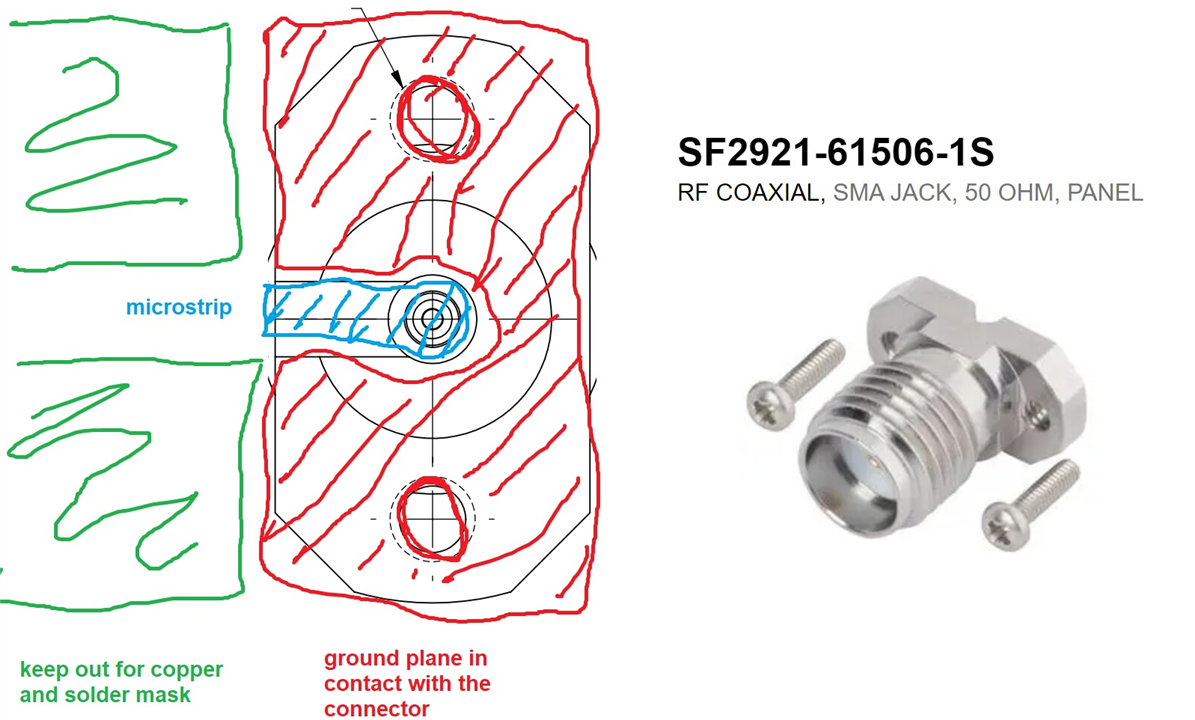
Part 2 of the exercise to create a custom footprint for the Amphenol /  SV Microwave SF2921-61506-1S   SMA coaxial connector. The previous post checked the possible layout. In this one, I'm drawing it in the footprint editor. This is the proposed design:

image
image source: Amphenol / SV Microwave documentation on element14 shop, annotated by me

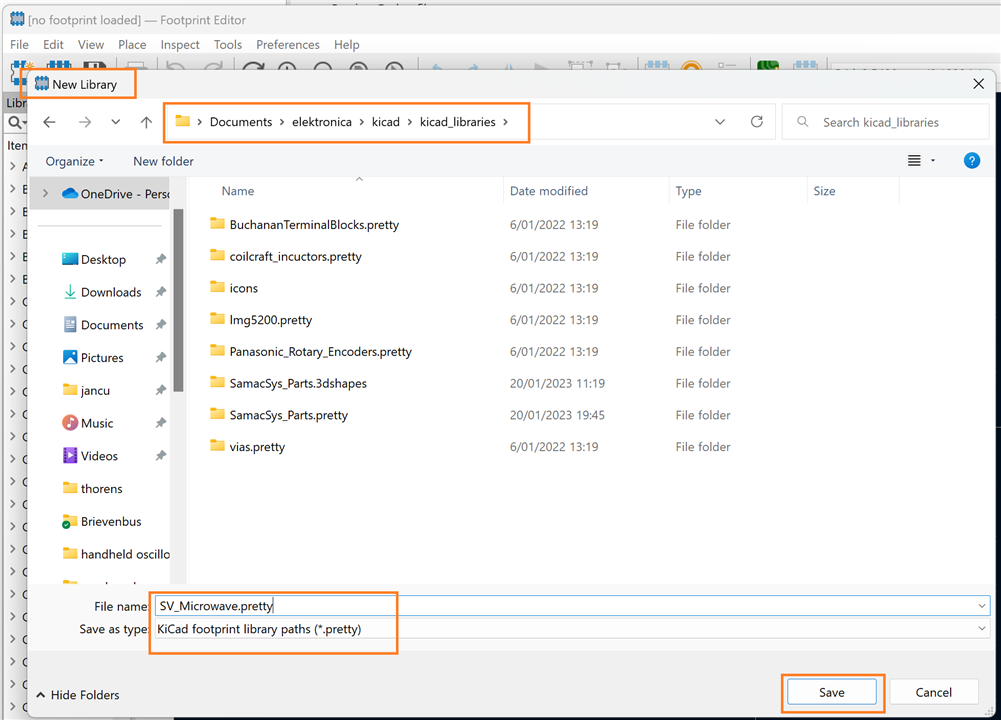
Create a new library and footprint

I have a directory with custom footprints that I made or collected. I'm creating anew one for SV Microwave.

image

Then I add a new footprint for the SF2921-61506-1S:

image

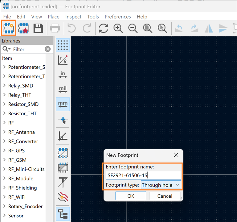
That's the starting point. I did a first save at that point.

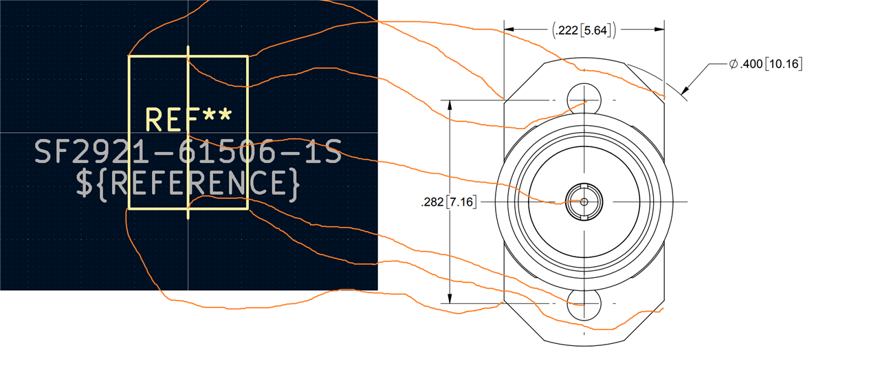
Step 1: initial outline

I try to start with a simple drawing that has a few reference points for later. Usually, I search for some square or rectangular simplification. In this case, I took the rectangle defined by the width of the connector and the distance of the drill holes for the screws. That immediately gives me 5 data points:

  • width
  • middle point where the spring sits
  • the two drill holes
  • middle point for the circle that defines the most outer vertical limits of the base
  • the mouse hole where the microstrip will escape

image

Quick check, compared to the stock footprint:
image

due to time limits, this post will be broken up in chunks. I try to keep these chunks big enough to document a step in the exercise.

  • Sign in to reply

Top Comments

  • scottiebabe
    scottiebabe 13 days ago +2
    You can play with kicads pcb calculator for some ballpark striplline/cpw geometry. You could target a 2-layer 0.6mm PCB or a 4+ layer where the top dielectric thickness is 0.1mm or 0.2 mm.
  • Jan Cumps
    Jan Cumps 13 days ago in reply to shabaz

    Example, where there's a copper and mask clearance around the signal line.

    image

    Once the traces leave the footprint area, the keepouts are defined in the PCB design.

    • Cancel
    • Vote Up 0 Vote Down
    • Sign in to reply
    • More
    • Cancel
  • scottiebabe
    scottiebabe 13 days ago

    You can play with kicads pcb calculator for some ballpark striplline/cpw geometry. You could target a 2-layer 0.6mm PCB or a 4+ layer where the top dielectric thickness is 0.1mm or 0.2 mm.

    image

    • Cancel
    • Vote Up +2 Vote Down
    • Sign in to reply
    • More
    • Cancel
  • Jan Cumps
    Jan Cumps 13 days ago in reply to Jan Cumps

    Extending that a little as guidance for the designer isn't hard:

    image

    The board designer will have to draw the keepout zones from there on, because I don't know where the traces head off to

    • Cancel
    • Vote Up 0 Vote Down
    • Sign in to reply
    • More
    • Cancel
  • Jan Cumps
    Jan Cumps 13 days ago in reply to shabaz

    Good point with removal of the solder mask. Some users will continue that on the entire trace anyway (kind of an optional thing). 

    That's the goal, but it's an exercise for the board designer. I stopped the predefined clearance at the outer boundaries of the connector's real estate.

    • Cancel
    • Vote Up 0 Vote Down
    • Sign in to reply
    • More
    • Cancel
  • Jan Cumps
    Jan Cumps 13 days ago in reply to shabaz

    I did the silkscreen with arch edges - although they will have to go because they interfere with the flush mounting of the connector on the pads.

    For the copper plains and the mask clearances, I used polygons with enough points to pretend they are a circle.

    The most difficult one is the location where the ground plain surrounds the centre pin. I've bodged that a little. When I know that the footprint is usable, I'll add some more polygon pins to mimic a circle form:

    image

    • Cancel
    • Vote Up 0 Vote Down
    • Sign in to reply
    • More
    • Cancel
>
element14 Community

element14 is the first online community specifically for engineers. Connect with your peers and get expert answers to your questions.

  • Members
  • Learn
  • Technologies
  • Challenges & Projects
  • Products
  • Store
  • About Us
  • Feedback & Support
  • FAQs
  • Terms of Use
  • Privacy Policy
  • Legal and Copyright Notices
  • Sitemap
  • Cookies

An Avnet Company © 2023 Premier Farnell Limited. All Rights Reserved.

Premier Farnell Ltd, registered in England and Wales (no 00876412), registered office: Farnell House, Forge Lane, Leeds LS12 2NE.

ICP 备案号 10220084.

Follow element14

  • Facebook
  • Twitter
  • linkedin
  • YouTube