


|
I'm going to draw my first footprint in the KiCad 7 Footprint editor.
I have experience with previous versions. To try out version 7, I'm going to make one for the Amphenol / SV Microwave SF2921-61506-1S SMA coaxial connector. In a first post on KiCad 7, I checked how to import a public domain footprint. This time I will try to mimic the microstripdesign that scottiebabe spotted in an application note. In this exercise, I will make it single layer, without vias. I don't want to prescribe that the microstrip's reference plane is the bottom layer of a PCB stack. I can always make a second version with reference plane and vias. |

Info collection and component details
As comparison, the imported footprint from previous post, the one from the application note with the best view, and the one from the note that I want to achieve:
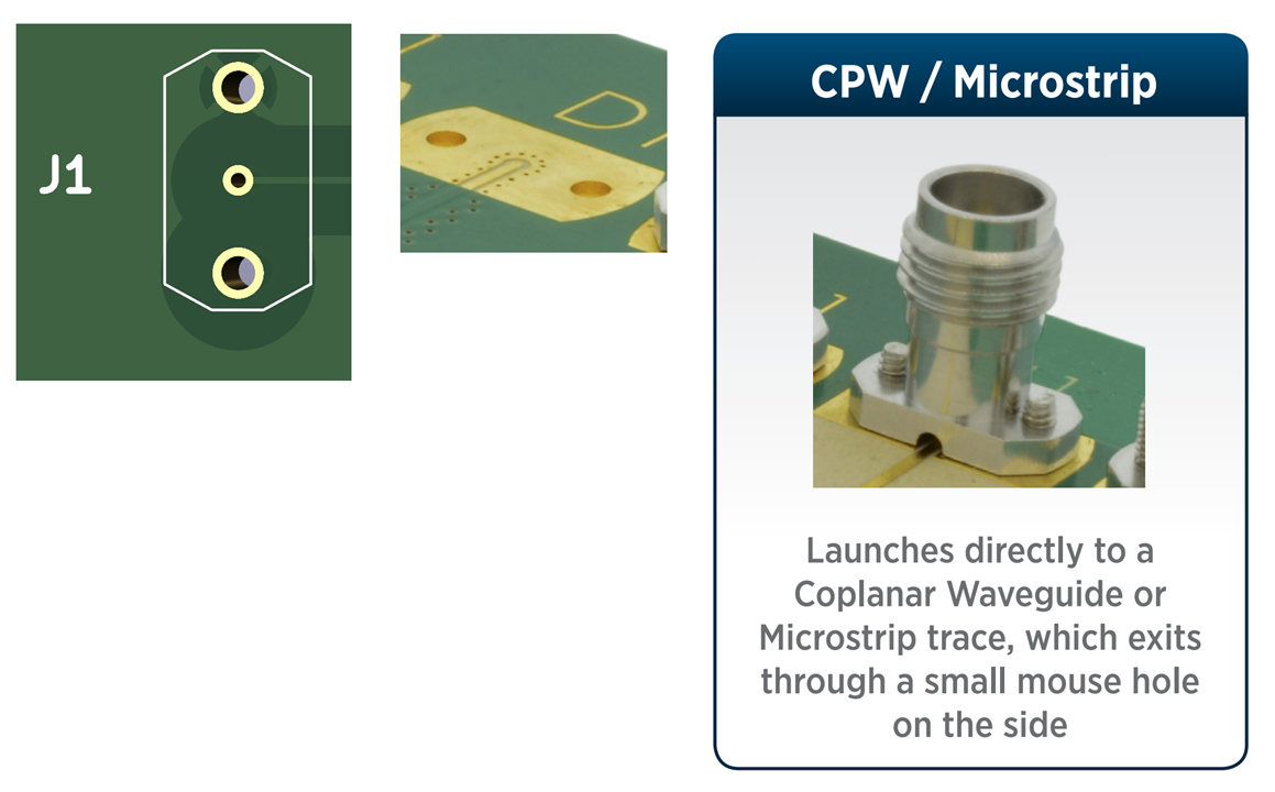
image source for 2 and 3: Amphenol / SV Microwave app note
The middle pin of the coax connector is best set on a PCB copper layer. It has spring action and does not need a hole. The housing should land on a copper pad that's the size of the connector's footprint. The middle pin's microstrip trace (conductor) should snake out via the opening in the underside of the connector.
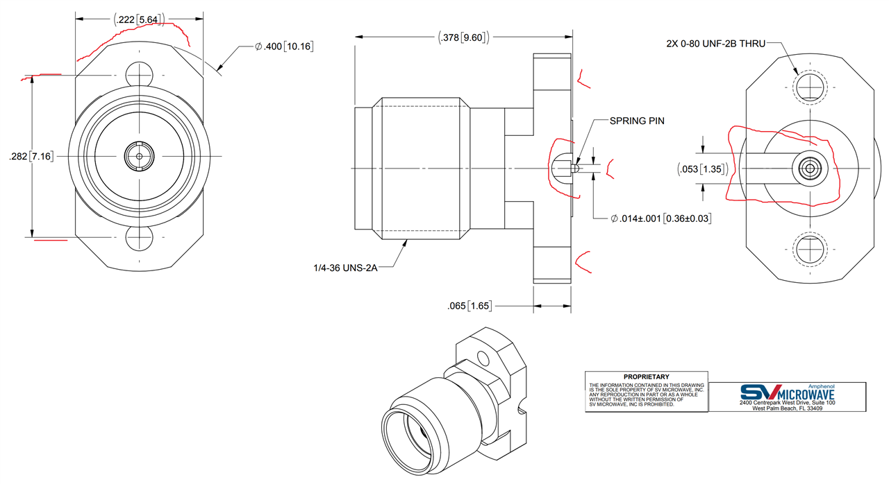
image source: Amphenol datasheet on element14 shop, annotated and edited by me
With this info, I should be able to define a footprint that looks approximately like this:

image source: Amphenol datasheet on element14 shop, annotated and edited by me
Blog Index
- Overview: Amphenol / SV Microwave SF2921-61506-1S SMA coaxial connector series
- Amphenol / SV Microwave SF2921-61506-1S SMA coaxial connector: behavior under vibration
- Create a custom footprint in KiCad 7 - 1: collect info and component details
- Create a custom footprint in KiCad 7 - 2a: create the footprint for an SMA coax connector with the editor - initial outline
- Create a custom footprint in KiCad 7 - 2b: create the footprint for an SMA coax connector with the editor - copper pour, solder mask clearance, holes, pads
- Use a LibraryLoader Footprint in KiCad 7
