


In the previous blog post, we built a HDMI source (output) controller inside our Spartan-7 FPGA and configured it using the Microblaze processor.
In this post we will add a physical HDMI output to our board, since the Arty-S7 does not have a HDMI output (or input) port.
First of all, we look at what we need on a higher level. If you look at a HDMI cable pinout, you will see there are 19 pins.

For a fully featured HDMI port, we should, ofcourse use all the pins. But that's not what we are going for here. We instead want to use the absolute minimum number of wires that we can get away with, which lets us display our FPGA's HDMI output on a computer/TV screen. So let's first talk about all the signals/wires that are NOT critical for us:
- Twisted pair shielding pins (one per twisted pair, 4 total) Good to have for immunity, EMC but not critical for short runs.
- CEC : Allows devices connected using HDMI to communicate (eg controlling multiple devices with one remote), but we don't need it.
- DDC (SDA, SCL): This is a I2C based protocol that allows HDMI source and receiver to talk to each other to query /publish capabilities (e.g supported resolutions). Not a necessity though.
- HPD (Hot Plug Detect): This lets a transmitter know when a receiver (e.g Screen/TV) is connected to it so that it can start transmitting. In our case we will be transmitting all the time so we can ignore it.
- A few Reserved pins
This leave us with the following 10 wires that are of interest to us:
- TMDS Clock +/- (1 twisted pair): The HDMI clock
- TMDS Data 0 +/- (1 twisted pair): Data 0
- TMDS Data 1 +/- (1 twisted pair): Data 1
- TMDS Data 2 +/- (1 twisted pair): Data 2
- Ground : Common ground for all functions (DDC, DEC, etc)
- (+)5V: Signals the receiver that a transmitter is present. In my experience some HDMI receivers will work without it, while others will require it.
So this gives us the 10 signals we need to carry on our HDMI wire/port.
Now let's look at how these signal requirements can be fulfilled on the FPGA side on our Arty S7.
HDMI uses TMDS signalling at a high data rate, which is (luckily) natively supported by the 7-series IO blocks. But to make use of it, we do need access to FPGA pads/ pins in a way that such high data rate can be supported. This means, among other possibilities, no resistors between the FPGA pad and the board IO pin which would slow down the slew rate (rise/fall speed) of the signals.
On the Arty S7, we have two types of PMOD ports:
1. High Speed PMOD
2. Low Speed PMOD
If we look at the Arty S7 schematic, specifically at the PMOD portion, we see the following:

On the right side PMODs (JC, JD) there are 200 Ohm resistors between the FPGA pad and the PMOD pin, while on the PMODs on the left side (JA, JB) they are instead populate with 0 Ohm resistors. This is what makes the right side PMODs (JC, JD) "low speed" and the left side PMODs (JA, JB) "high speed" IOs since the later do not have resistors slowing down the signal slew rates.
So from here we establish that we can use either JA or JB for our HDMI transmitter port.
Now Let's revisit the constraints we used in our design:
set_property -dict {PACKAGE_PIN M18 IOSTANDARD TMDS_33} [get_ports hdmi_tx_0_clk_p]
set_property -dict {PACKAGE_PIN M16 IOSTANDARD TMDS_33} [get_ports {hdmi_tx_0_data_p[2]}]
set_property -dict {PACKAGE_PIN M14 IOSTANDARD TMDS_33} [get_ports {hdmi_tx_0_data_p[1]}]
set_property -dict {PACKAGE_PIN L17 IOSTANDARD TMDS_33} [get_ports {hdmi_tx_0_data_p[0]}]
In the constraints file we are doing two things:
1. Setting the pin for each signal
2. Assigning the TMDS IO standard to each pin
For differential pairs, we only need to specify the positive pin for a pair. The negative pin is automatically assigned, and cannot be changed. In the device datasheet, you will see these pin pairs with prefix of _N and _P. Note that when connecting the physical wires, BOTH the _P and _N need to be connected. Not only that, we need to use twisted wires for each pair, with 100Ohm differential impedance.
If you compare the assinged pins to the Arty S7 schematic, you will notice that we are using the PMOD connector "JA" for this. Why did we use JA and not JB? Well, the reason is that JB has some pins that are SRCC(single region clock capable), MRCC (multiple region clock capable). These are useful if we want to input an external clock into the FPGA. For example, if we want to add a HDMI receiver to our design later. So although we can use JB for our HDMI transmitter just as well as JA, we leave JB in case we decide to add a HDMI input to our design later on.
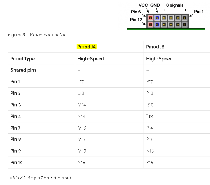
Luckily, our Arty S7 is capable of 4 differential pairs on the "JA" PMOD port, and additional pins for Ground and +3.3V. We will use the 4 differential pairs for TMDS (Clock, data 0-2), Ground will connect to Ground on the PMOD. For the +5V signal, we will first try leaving it unconnected to see if that works with our screen, otherwise we will try supplying it with 3.3V from PMOD, or 5V from one of the Arduino compatible headers on the Arty-S7 hoping that the voltage exceed the HIGH threshold for the input circuitry. Note that this +5V is not for powering up the receiver, but rather to signal to the receiver that a transmitter is connected on the HDMI port. As i mentioned earlier, based on my own experience, some receivers require it while other receivers will not require it as long as they see valid signals on the TMDS pairs.
Now that we know what connects where, let's build the cable. For my cable, I had two options:
1. Cut a HDMI cable into two and then solder one half to a two-row 2.54mm header (same as PMOD).
2. Build a cable from scratch, using twisted wires, HDMI connectors and PMOD compatible header.
The problem with first approach was that the actual wires in most HDMI cables are very thin and fragile, and break easily once you have them outside the cable (for soldering to pins, for example). I tried this first, but didn't like the outcome. So instead I opted for building a cable from scratch.
First, I built a wire bundle with 4x twisted pairs (for TMDS signals) and 2 more wires (for Ground, +5V). Then, I soldered them to the respective pins on bare HDMI connectors and made a HDMI male-to-male cable.


This way, I could test the cable and make sure it works fine, before I cut it and solder one half to 2.54mm header pins.

Once this was tested, I cut it in the middle and soldered one half to a dual-row 2.54mm header (compatible with PMOD spacing). The final result looks as following:

Now, all that was left was to connect this cable on one end to the "JA" PMOD, other end to the HDMI input of my TV, and compile and run the Vitis program that we created in the previous post.

In a few seconds, a 640x480/60Hz test pattern appeared on the screen.


Congratulations! We have just turned our Arty-S7 into an imaging capable system even though the board doesn't have any HDMI output port. THIS is the flexibility and power of FPGAs!


