element14 Community
element14 Community
    Register Log In
  • Site
  • Search
  • Log In Register
  • Community Hub
    Community Hub
    • What's New on element14
    • Feedback and Support
    • Benefits of Membership
    • Personal Blogs
    • Members Area
    • Achievement Levels
  • Learn
    Learn
    • Ask an Expert
    • eBooks
    • element14 presents
    • Learning Center
    • Tech Spotlight
    • STEM Academy
    • Webinars, Training and Events
    • Learning Groups
  • Technologies
    Technologies
    • 3D Printing
    • FPGA
    • Industrial Automation
    • Internet of Things
    • Power & Energy
    • Sensors
    • Technology Groups
  • Challenges & Projects
    Challenges & Projects
    • Design Challenges
    • element14 presents Projects
    • Project14
    • Arduino Projects
    • Raspberry Pi Projects
    • Project Groups
  • Products
    Products
    • Arduino
    • Avnet & Tria Boards Community
    • Dev Tools
    • Manufacturers
    • Multicomp Pro
    • Product Groups
    • Raspberry Pi
    • RoadTests & Reviews
  • About Us
  • Store
    Store
    • Visit Your Store
    • Choose another store...
      • Europe
      •  Austria (German)
      •  Belgium (Dutch, French)
      •  Bulgaria (Bulgarian)
      •  Czech Republic (Czech)
      •  Denmark (Danish)
      •  Estonia (Estonian)
      •  Finland (Finnish)
      •  France (French)
      •  Germany (German)
      •  Hungary (Hungarian)
      •  Ireland
      •  Israel
      •  Italy (Italian)
      •  Latvia (Latvian)
      •  
      •  Lithuania (Lithuanian)
      •  Netherlands (Dutch)
      •  Norway (Norwegian)
      •  Poland (Polish)
      •  Portugal (Portuguese)
      •  Romania (Romanian)
      •  Russia (Russian)
      •  Slovakia (Slovak)
      •  Slovenia (Slovenian)
      •  Spain (Spanish)
      •  Sweden (Swedish)
      •  Switzerland(German, French)
      •  Turkey (Turkish)
      •  United Kingdom
      • Asia Pacific
      •  Australia
      •  China
      •  Hong Kong
      •  India
      •  Korea (Korean)
      •  Malaysia
      •  New Zealand
      •  Philippines
      •  Singapore
      •  Taiwan
      •  Thailand (Thai)
      • Americas
      •  Brazil (Portuguese)
      •  Canada
      •  Mexico (Spanish)
      •  United States
      Can't find the country/region you're looking for? Visit our export site or find a local distributor.
  • Translate
  • Profile
  • Settings
FPGA
  • Technologies
  • More
FPGA
Blog Entering The World Of FPGA's with a DEO-NANO P0082 - Part 3
  • Blog
  • Forum
  • Documents
  • Quiz
  • Events
  • Polls
  • Files
  • Members
  • Mentions
  • Sub-Groups
  • Tags
  • More
  • Cancel
  • New
Join FPGA to participate - click to join for free!
  • Share
  • More
  • Cancel
Group Actions
  • Group RSS
  • More
  • Cancel
Engagement
  • Author Author: Former Member
  • Date Created: 29 Jul 2017 3:49 PM Date Created
  • Views 2681 views
  • Likes 16 likes
  • Comments 6 comments
  • p0082
  • de0 nano
  • terasic
  • de0-nano
  • enterfpga
  • p0082(terasic)
  • terasic p0082 de0-nano fpga development kit
Related
Recommended

Entering The World Of FPGA's with a DEO-NANO P0082 - Part 3

Former Member
Former Member
29 Jul 2017

  If your looking to get into FPGA development and have been following my blogs, this is probably the post that you should pay most attention to as it's likely to make clear the design process.


So far I've followed the quick start guide,  downloaded the recommended software and installed the demo bitstreams onto the deo-nano development board. For clarification, a bitstream (or bit stream) is the name of your compiled project that gets transferred onto the FPGA device.


Now it's time to follow the my-first-fpga guide to create my first ever FPGA project, its a foolproof step by step guide which takes us from the very beginning of making a project through to downloading that compiled project onto the deo-nano development board.


Forget any other software that comes with the board, all were interested in is the Altera Quartus2 design suite, this has everything we need including a compiler and hardware programmer. This one thing does it all.


Here's a quick run through of the steps used to develop an FPGA application:


1) Create a project with the wizard, giving it a name and telling it which FPGA you are using.

2) Add a Block Diagram/Schematic to the project (this is similar to a schematic editor on PCB design software where components can be added, moved and connected with wires)

3) The objects on the schematic are created by using a programming language called Verilog HDL, it has similarities to other programming languages.

4) Once an object has been created in Verilog HDL, it shows up as a symbol on the schematic. Wires can be connected between these objects using inputs and outputs described in the programming.

5) Symbols of input / output pins are created on the schematic to represent the physical pins to allow interaction with the real world. These can be connected to the inputs/outputs of our object.

6) The input/output pin symbols are given names, a pin planner allows us to point those names to the physical pins on the fpga.

7) Compile the project.

8) program the bitstream (the output of the compiler) onto the fpga


Ok, there are a couple of other bits but thats a general overview and hopefully it outlines the process that people new to FPGA's can understand. Its basically very similar to making a circuit diagram in a pcb design package. Where the components have internal functions defined by a programming language. Anybody who used Javabeans and played with the Beanbox will be very comfortable using this!


So lets first look at the Block Diagram/Schematic view


image


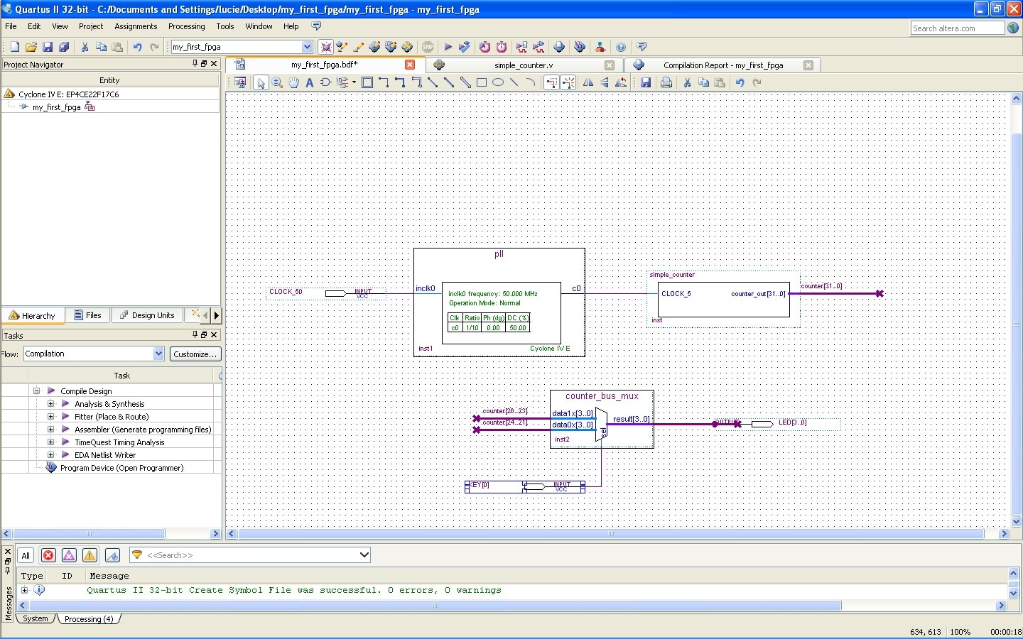
This is the completed schematic for my project, The object in the top right labelled "simple_counter" is an object that I made in Verilog HDL following an example whereas the other two main objects are pre-made objects that Altera provides (A wizard can help set them up and tailor them for your needs).


Coming out of the right hand side of "simple_counter" is a wire labelled "counter", Because the wires going into the left of the "counter_bus_mux" are also labelled "counter" these are all symbollically linked so its as if all of those wires are connected to each other.


The smaller objects labelled "CLOCK_50", "KEY[0]" and "LED[3..0]" are all symbollic of physical pins on the fpga, these get assign or mapped to real life pins later in the process.


image


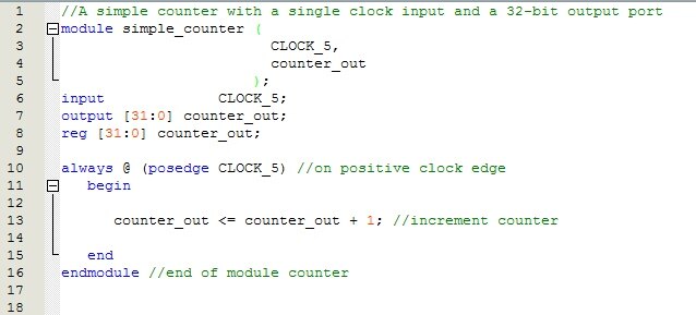
Here's the Verilog HDL code that went into making the "simple_counter" object in the schematic above, as you can see it has an input and a output described, you can see these displayed in the schematic above. Notice how the structure is similar to other programming languages and it's pretty easy to follow.


Once this object has been saved we can add it to the schematic and link other objects to it, the design suite draws the object for us, we don't need to do anything like that ourselves.


image


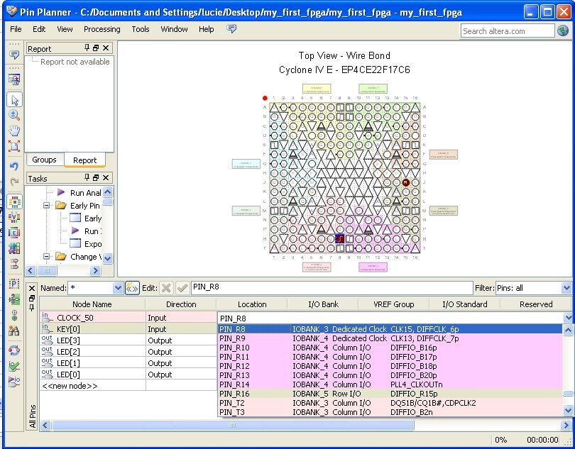
Once our schematic is complete, its time to launch the Pin Planner. If you look at the table at the bottom of the Pin Planner under node names, we can see the names of the input/output pins in our schematic above. In the location box is where we assign the pin in the schematic to the desired pin on the physical FPGA. In this picture, I double clicked the location box for "CLOCK_50" and a drop down list of all of the pins on our fpga device appeared. I selected PIN_R8 which is a dedicated clock pin, so looking back at the schematic we can see that CLOCK_50 is going to be turned on and off by a clock source on the fpga.


image


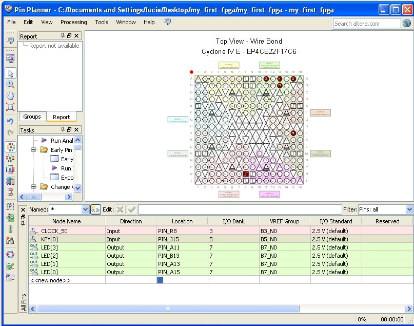
Heres the completed pin assignment. This can be opened up at anytime during the design process to assign new input/output pins.


Once this is done your project is finished and its simply a case of clicking the compile button, plugging the de0-nano into a USB port and copying the compiled bitstream program onto the fpga using the programmer in the design suite. I have included any pictures for the process as it really is simple and self explanatory. There are pictures and a step by step guide in the my-first-fpga document but I have included a picture of the compiler report that was generated:


image


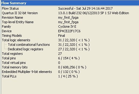
As you can see, very few of the fpga's resources were used to make this project.


I'm going to try and explain the schematic (and hopefully get it right).

1) An external clock source is fed into a PLL(phase locked loop) element. This takes a 50mhz clock which is pulsing this pin on/off and slows it down. The output of this PLL goes into the simple counter, the single output of this counter is symbolic of a 32bit bus. The counter element itself increments the 32bit bus like it would a 32bit variable. From that 32-bit bus, just 8 of those bits are fed into the "counter_bus_mux". Im not sure exactly how that part works but it takes the data from those 8-bits and converts it into 4bits then displays it onto 4 led's.


Hopefully I got that right, if not then please feel free to explain better in the comments below!!


Heres a quick video of the results of this project:


You don't have permission to edit metadata of this video.
Edit media
x
image
Upload Preview
image


And that's it for today! Tomorrow Im going to go Lone Ranger and try to get this binary counter displaying on all 8 LED's rather than just 4 before I get bogged down reading the full user manual.


Oh! Maybe I should mention that I completed this project in under an hour, there appears to be a lot to it but realistically it was easier than I anticipated!!

  • Sign in to reply

Top Comments

  • Former Member
    Former Member over 8 years ago in reply to johnbeetem +3
    Thats great, thanks for explaining!! The Mux is one of the autogenerated components so its not immediately obvious what its doing. If I just remove that multiplexer and map 8 single consecutive bits from…
  • johnbeetem
    johnbeetem over 8 years ago in reply to Former Member +3
    lucie tozer wrote: If I just remove that multiplexer and map 8 single consecutive bits from the output of "counter" each to an individual LED would that produce an 8-bit counter with a pause in between…
  • johnbeetem
    johnbeetem over 8 years ago +2
    Lucie wrote: From that 32-bit bus, just 8 of those bits are fed into the "counter_bus_mux". I'm not sure exactly how that part works but it takes the data from those 8-bits and converts it into 4bits then…
Parents
  • johnbeetem
    johnbeetem over 8 years ago

    Lucie wrote: From that 32-bit bus, just 8 of those bits are fed into the "counter_bus_mux". I'm not sure exactly how that part works but it takes the data from those 8-bits and converts it into 4bits then displays it onto 4 LEDs.


    Hopefully I got that right, if not then please feel free to explain better in the comments below!!

    Here's my understanding of the schematic.


    A 2:1 mux (multiplexer) is an "if-then-else" expression.  It has two data inputs (the 4-bit buses data0x[3..0] and data1x[3..0]) and one select input "sel".  The output (the 4-bit bus result[3..0]) is the data input selected by "sel": "result = if sel then data1x else data0x", or if you like C conditional expresions: "result = sel? data1x: data0x".


    In the schematic, data0 is connected to counter[24..21] and data1 is connected to counter[20..23] (note the bit reversal), in each case extracting 4 consecutive bits from the 32-bit counter[31..0].  "sel" is connected to an external push-button KEY[0].  The default behavior (KEY[0] = 0) is a 4-bit binary counter in the LEDs.  If you press the button (KEY[1] = 1), the order of the four bits reverse (LSb on left versus LSb on right) and the counter speed doubles.  Fun demo!  It's not clear from the schematic whether KEY and LEDs are active-high or active-low, and the left-to-right (or top-to-bottom) order of the LEDs.

    • Cancel
    • Vote Up +2 Vote Down
    • Sign in to reply
    • More
    • Cancel
  • Former Member
    Former Member over 8 years ago in reply to johnbeetem

    Thats great, thanks for explaining!! The Mux is one of the autogenerated components so its not immediately obvious what its doing.


    If I just remove that multiplexer and map 8 single consecutive bits from the output of "counter" each to an individual LED would that produce an 8-bit counter with a pause in between each counting cycle?


    edit

    I suppose I should just give it a try and see what happens!!

    • Cancel
    • Vote Up +3 Vote Down
    • Sign in to reply
    • More
    • Cancel
Comment
  • Former Member
    Former Member over 8 years ago in reply to johnbeetem

    Thats great, thanks for explaining!! The Mux is one of the autogenerated components so its not immediately obvious what its doing.


    If I just remove that multiplexer and map 8 single consecutive bits from the output of "counter" each to an individual LED would that produce an 8-bit counter with a pause in between each counting cycle?


    edit

    I suppose I should just give it a try and see what happens!!

    • Cancel
    • Vote Up +3 Vote Down
    • Sign in to reply
    • More
    • Cancel
Children
  • johnbeetem
    johnbeetem over 8 years ago in reply to Former Member

    lucie tozer wrote:


    If I just remove that multiplexer and map 8 single consecutive bits from the output of "counter" each to an individual LED would that produce an 8-bit counter with a pause in between each counting cycle?


    I suppose I should just give it a try and see what happens!!

    You won't get pauses -- you'll just get an 8-bit counter instead of a 4-bit counter.  If you want to pause, you need something like (in Verilog): "LEDs = counter[24]? counter[23:20]: 4'b0000" which means if counter bit 24 is 1 the four LEDs count but if counter[24] is 0 they show the value 0000 for 16 ticks.


    And yes -- do play!  Just keep saving your work so you can get back to something that works after experimenting.


    I see you haven't said much about simulation.  I almost never do simulation myself, and with decent development boards IMO there's rarely a need to do so.

    • Cancel
    • Vote Up +3 Vote Down
    • Sign in to reply
    • More
    • Cancel
element14 Community

element14 is the first online community specifically for engineers. Connect with your peers and get expert answers to your questions.

  • Members
  • Learn
  • Technologies
  • Challenges & Projects
  • Products
  • Store
  • About Us
  • Feedback & Support
  • FAQs
  • Terms of Use
  • Privacy Policy
  • Legal and Copyright Notices
  • Sitemap
  • Cookies

An Avnet Company © 2025 Premier Farnell Limited. All Rights Reserved.

Premier Farnell Ltd, registered in England and Wales (no 00876412), registered office: Farnell House, Forge Lane, Leeds LS12 2NE.

ICP 备案号 10220084.

Follow element14

  • X
  • Facebook
  • linkedin
  • YouTube