element14 Community
element14 Community
    Register Log In
  • Site
  • Search
  • Log In Register
  • Members
    Members
    • Benefits of Membership
    • Achievement Levels
    • Members Area
    • Personal Blogs
    • Feedback and Support
    • What's New on element14
  • Learn
    Learn
    • Learning Center
    • eBooks
    • STEM Academy
    • Webinars, Training and Events
    • Learning Groups
  • Technologies
    Technologies
    • 3D Printing
    • Experts & Guidance
    • FPGA
    • Industrial Automation
    • Internet of Things
    • Power & Energy
    • Sensors
    • Technology Groups
  • Challenges & Projects
    Challenges & Projects
    • Design Challenges
    • element14 presents
    • Project14
    • Arduino Projects
    • Raspberry Pi Projects
    • Project Groups
  • Products
    Products
    • Arduino
    • Dev Tools
    • Manufacturers
    • Raspberry Pi
    • RoadTests & Reviews
    • Avnet Boards Community
    • Product Groups
  • Store
    Store
    • Visit Your Store
    • 'Choose another store...'
      • Europe
      •  Austria (German)
      •  Belgium (Dutch, French)
      •  Bulgaria (Bulgarian)
      •  Czech Republic (Czech)
      •  Denmark (Danish)
      •  Estonia (Estonian)
      •  Finland (Finnish)
      •  France (French)
      •  Germany (German)
      •  Hungary (Hungarian)
      •  Ireland
      •  Israel
      •  Italy (Italian)
      •  Latvia (Latvian)
      •  
      •  Lithuania (Lithuanian)
      •  Netherlands (Dutch)
      •  Norway (Norwegian)
      •  Poland (Polish)
      •  Portugal (Portuguese)
      •  Romania (Romanian)
      •  Russia (Russian)
      •  Slovakia (Slovak)
      •  Slovenia (Slovenian)
      •  Spain (Spanish)
      •  Sweden (Swedish)
      •  Switzerland(German, French)
      •  Turkey (Turkish)
      •  United Kingdom
      • Asia Pacific
      •  Australia
      •  China
      •  Hong Kong
      •  India
      •  Korea (Korean)
      •  Malaysia
      •  New Zealand
      •  Philippines
      •  Singapore
      •  Taiwan
      •  Thailand (Thai)
      • Americas
      •  Brazil (Portuguese)
      •  Canada
      •  Mexico (Spanish)
      •  United States
      Can't find the country/region you're looking for? Visit our export site or find a local distributor.
  • Translate
  • Profile
FPGA
  • Technologies
  • More
FPGA
Blog Exploring 7 Series MIG Part - 1
  • Blog
  • Forum
  • Documents
  • Events
  • Polls
  • Files
  • Members
  • Mentions
  • Sub-Groups
  • Tags
  • More
  • Cancel
  • New
FPGA requires membership for participation - click to join
Blog Post Actions
  • Subscribe by email
  • More
  • Cancel
  • Share
  • Subscribe by email
  • More
  • Cancel
Group Actions
  • Group RSS
  • More
  • Cancel
Engagement
  • Author Author: hrishi98
  • Date Created: 1 Jun 2022 5:21 PM Date Created
  • Views 2754 views
  • Likes 9 likes
  • Comments 4 comments
  • arty-s7
  • 7 Ways to Leave Your Spartan-6
  • ddr
  • Spartan_Migration
Related
Recommended

Exploring 7 Series MIG Part - 1

hrishi98
hrishi98
1 Jun 2022
Exploring 7 Series MIG Part - 1

Exploring 7 Series MIG Part - 1

Hello, last week I received the Arty S7 board as part of the 7 Ways to Leave Your Spartan 6 Challenge, on power-up LEDs started blinking using the preloaded binaries. Happy to see it working, but I was confused looking at the DDR part on the board. Digilent advertised it to be MT41K128M16XX-15E from Micron, but the part present was PMF511816EBR from Piecemakers. After looking into the timing parameters of both the parts they looked the same, so I decided to test the DDR to make sure it really works.

7 Series FPGAs do not have hard memory controllers instead, they have hard PHY which exposes DFI Interface. DDR Controllers must be used to act as a mediator to provide access between user interfaces say AXI and DFI. Xilinx provides Memory Interface Generator (MIG) memory controller for this purpose.

7 series MIG IP configuration is a bit complicated compared to the new generation MPSoC MIG. Initially, I was not able to find example designs for Arty, and even Arty S7 board automation seems to be broken. So here is the documentation on running the SDK Memory Tests application for initial testing of DDR.

Vivado project creation steps are skipped to reduce the length of this blog, create a new project by selecting the Arty S7-50 board and create a new block design before proceeding.

Click on the Board option under the sources tab. Double click on System Reset and click OK.

image

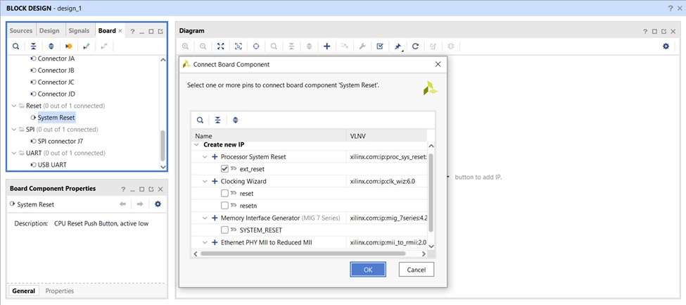
Processor System Reset IP will be added to the canvas. Double click on System Clock and Click OK.

image

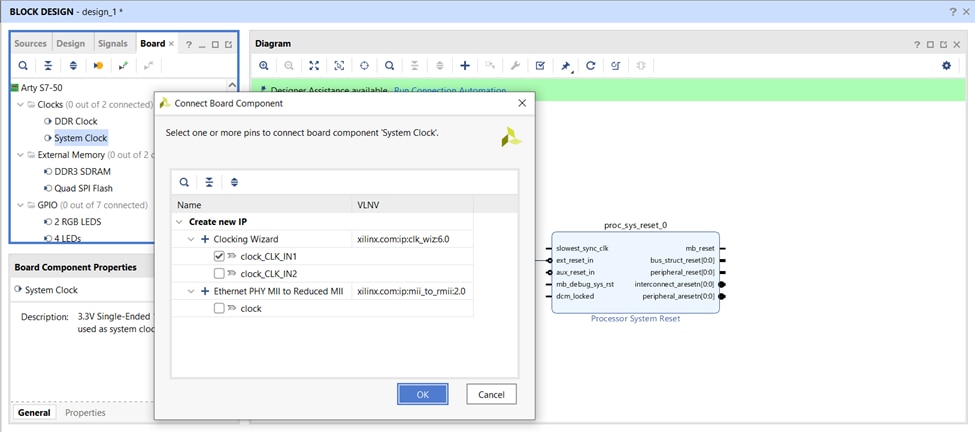
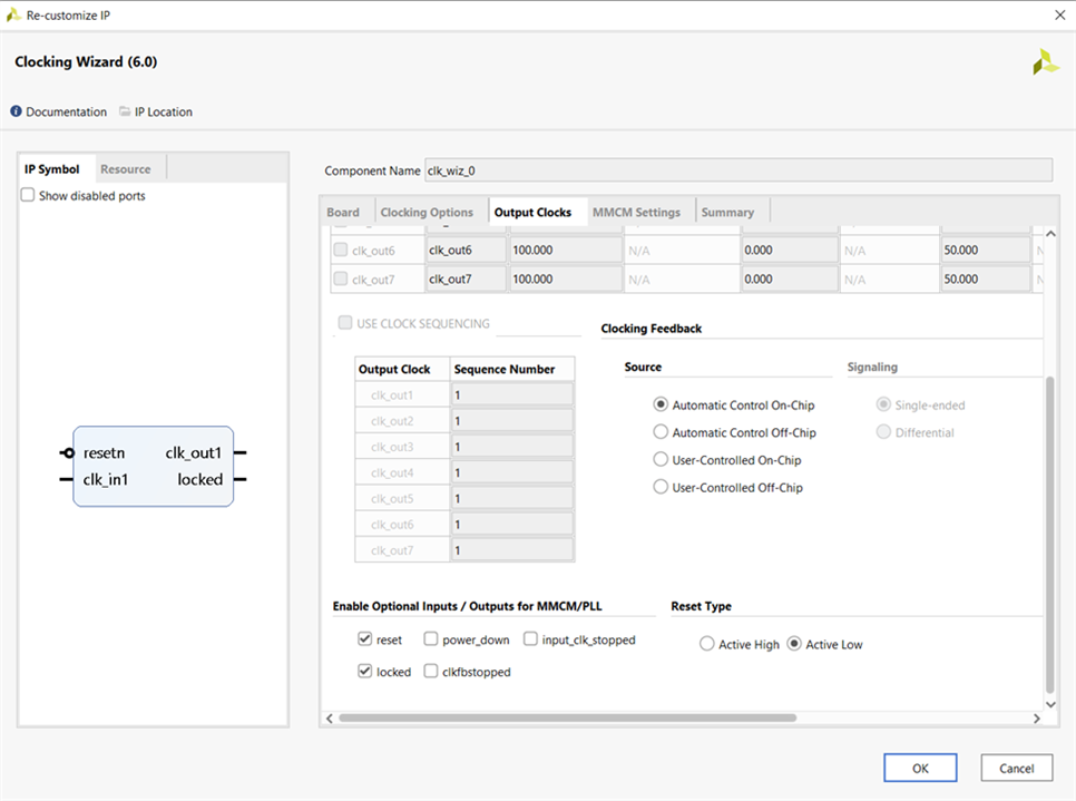
A clocking wizard which takes in a 12MHz clock and generates a 100MHz clock will be added. Double click on the clocking wizard and change reset polarity to active low, as the System Reset present on Arty is active low reset.

image

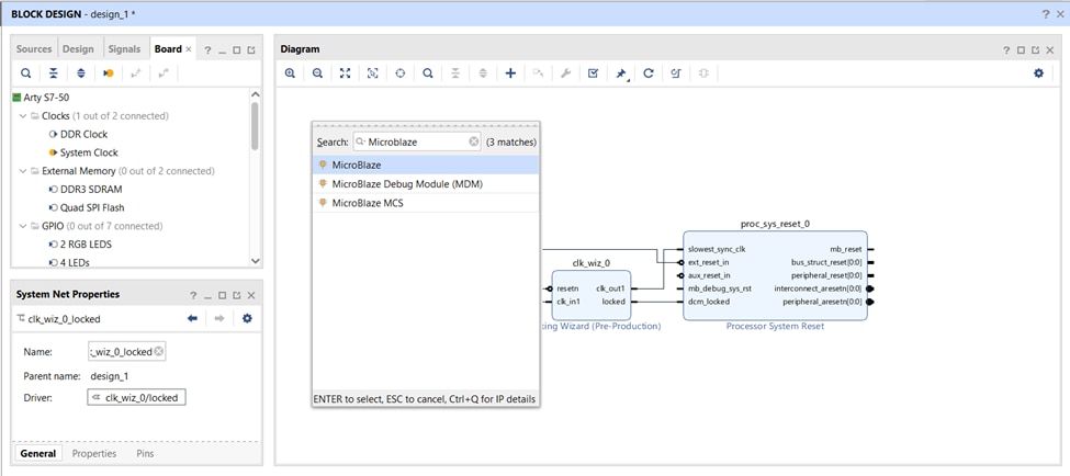
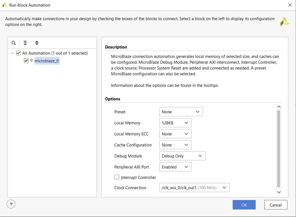
Now run connection automation to make necessary connections. Add MicroBlaze to the IP canvas.

image

Run Block Automation to add the necessary debug module and BRAM. Make sure the following settings are selected while running automation.

image

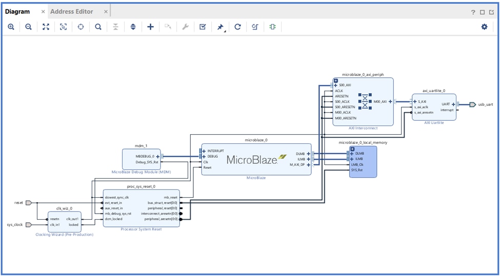
Add AXI UART Lite to IP canvas, Run Connection Automation. Now base design with MicroBlaze and UART is ready.

image

Arty S7-50 has a 250M Bytes (128M bits x 16) DDR in older versions of boards MT41K128M16XX-15E from Micron was used but the latest boards have PMF511816EBR from Piecemakers. Both parts have the same timing parameters, even new chips are capable of working at 1.35V.

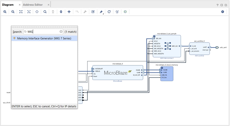
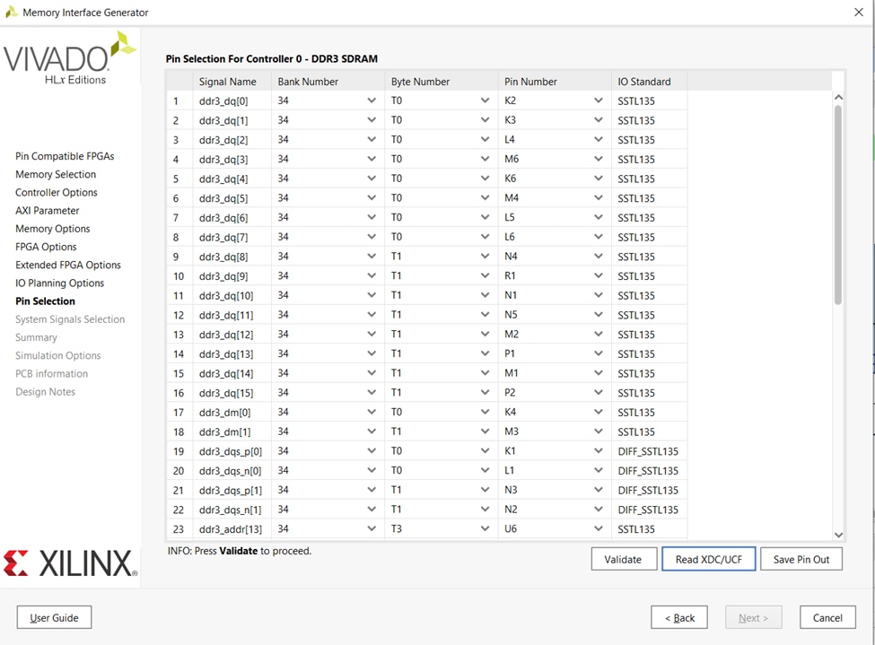
Instead of running block automation let us configure MIG IP manually. Before proceeding make sure to download UCF File from Digilent Github. The file contains all DDR pin details and will be used later.

Add Memory Interface Generator to IP canvas.

 image

Double click on MIG IP and click Next to skip the welcome page.

image

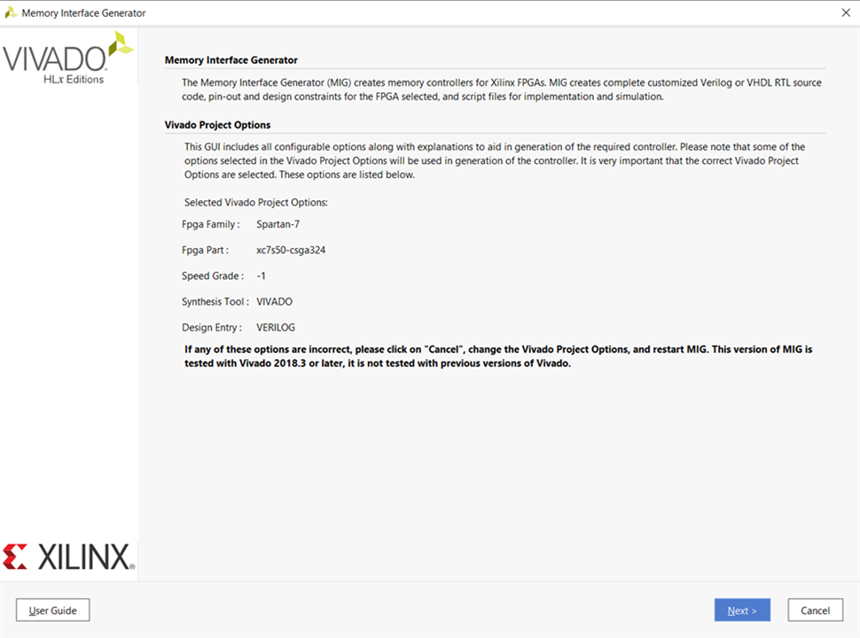
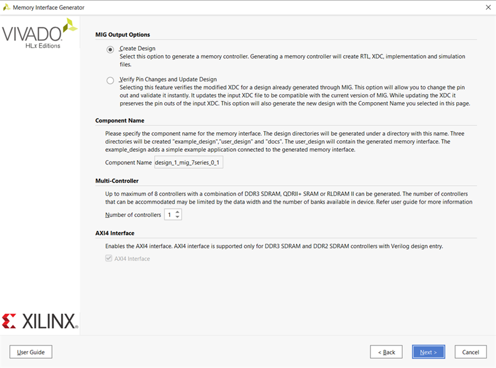
Make sure create design is selected and click on Next.

image

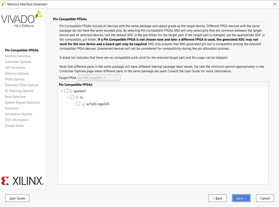
We will provide pin information in later step, so click on next instead of specifying compatible pins.

image

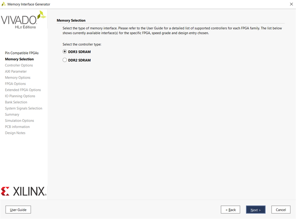
Select DDR3 SDRAM and click on Next.

image

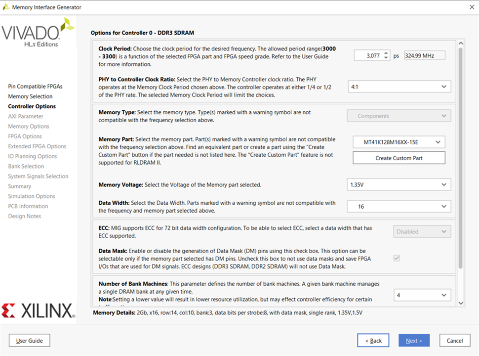
DDR will be operated at a 650Mbps data rate, with data width being 16 bits, 324.99 MHz clock must be fed. Make the following selections under the Options for Controller tab and click Next.

Clock Period: 3077 (324.99 MHz), This is the clock that will be provided as input for the DDR chip i.e., physical layer memory clock frequency.

PHY to Controller Clock Ratio: 4:1, Ration of physical layer clock frequency to user interface clock frequency.

Memory Part: MT41K128M16XX-15E, Memory part used in the board as Piecemakers part is not displayed select Micron part.

Memory Voltage 1.35 V, Voltage at which DDR chip will be operated.

Data Width: 16, Data width of the DDR chip.

ORDERING: Normal, this mode allows the memory controller to reorder commands to achieve maximum possible efficiency.

 image

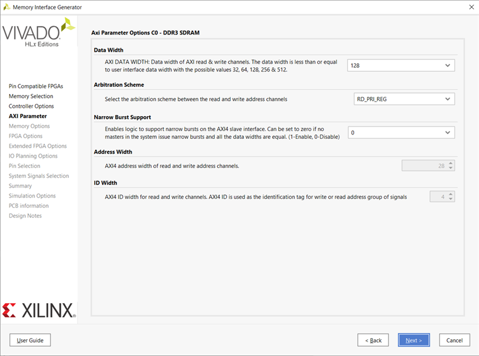
Settings under the AXI Parameter Options tab will not be changed so click on Next.

 image

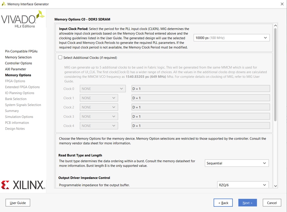
Make the following selections under the Memory Options tab and click Next.

Input Clock Period: 10000ps (100MHz), This is the reference clock provided to the MIG controller.

Output Driver Impedance Control: RZQ/6

RTT nominal – On Die Termination (ODT): RZQ/6

image

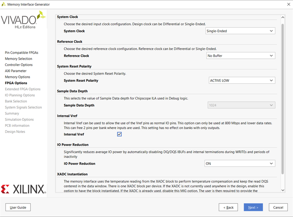
Select System Clock options as shown below click Next.

System Clock: Single Ended, Arty S7 board has a 100MHz single-ended 100MHz clock.

Reference Clock: No Buffer

System Reset Polarity: Active Low, Arty S7 has an active low system reset.

Internal Vref: Tik Mark

XADC Instantiation: Enabled

image

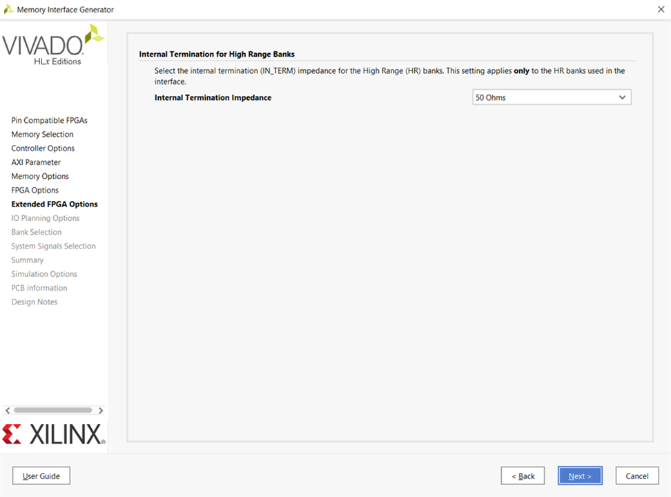
Select Internal Termination Impedance: 50 Ohms and click Next.

image

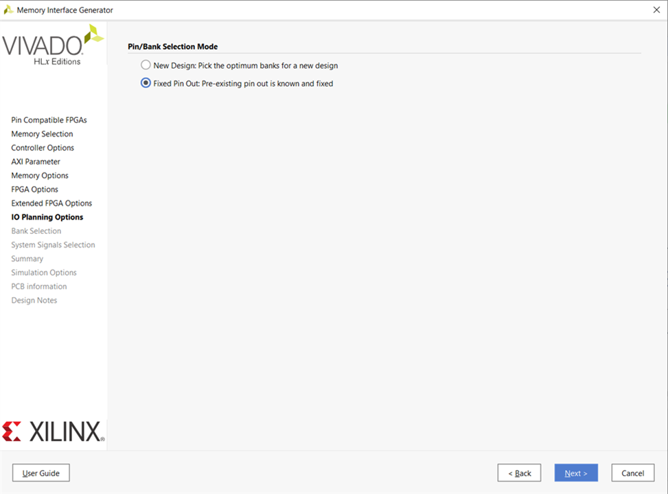
Select Fixed Pin Out: Pre-Existing pinout is known and fixed and Click Next.

image

Now it’s time to import the UCF file previously downloaded select Read XDC/UCF click on Validate and click Next.

image

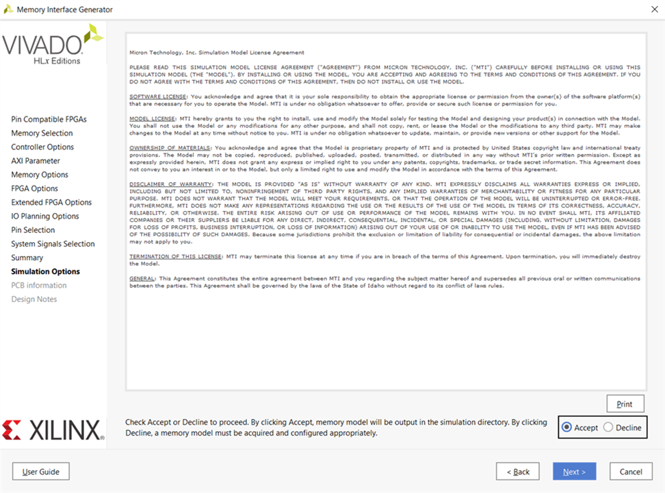
Keep on clicking Next until the Agreement window appears, accept the terms and click Next.

 image

Click Next.

image

Click on Generate.

 image

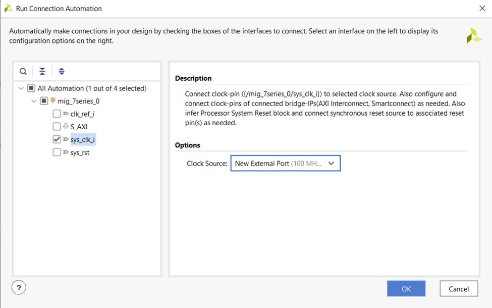
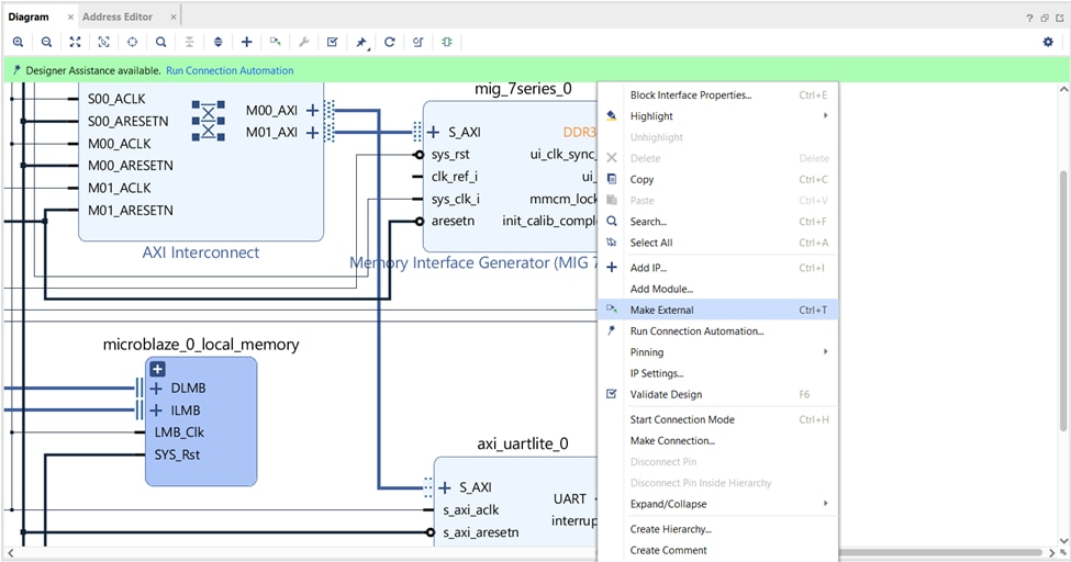
Run connection automation by selecting New External Port for DDR sys_clk_i.

image

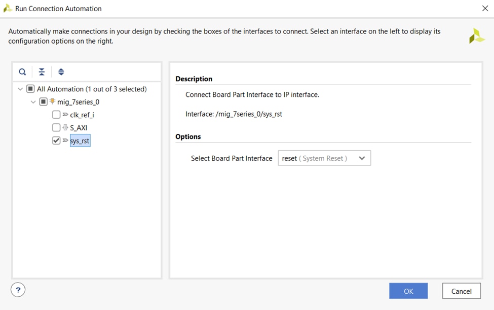
Run connection automation by selecting system reset as DDR reset.

image

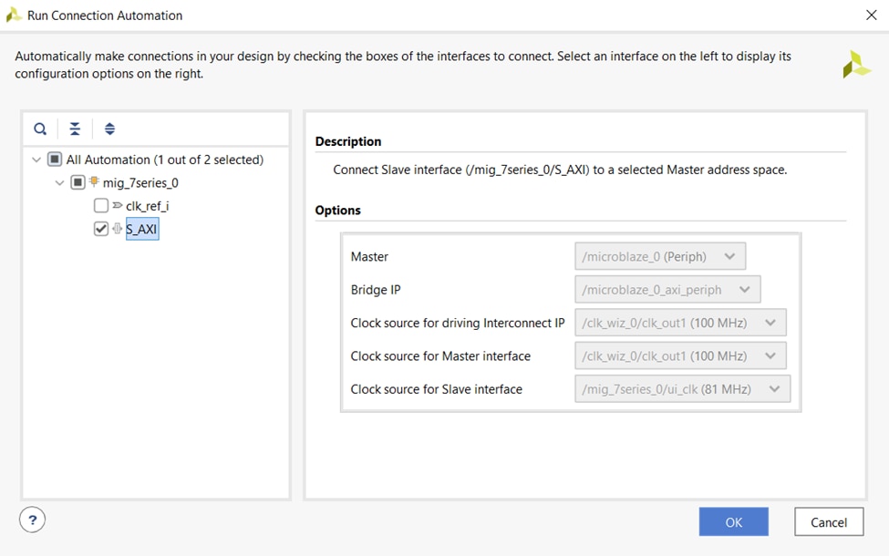
Similarly run connection automation by selecting DDR AXI Interface. AXI Interface will be running on 81.247969 MHz ui_clk generated by DDR MIG. This clock is ¼ th of physical interface clock as mentioned previously.

image

Right click on DDR port and make it external.

image

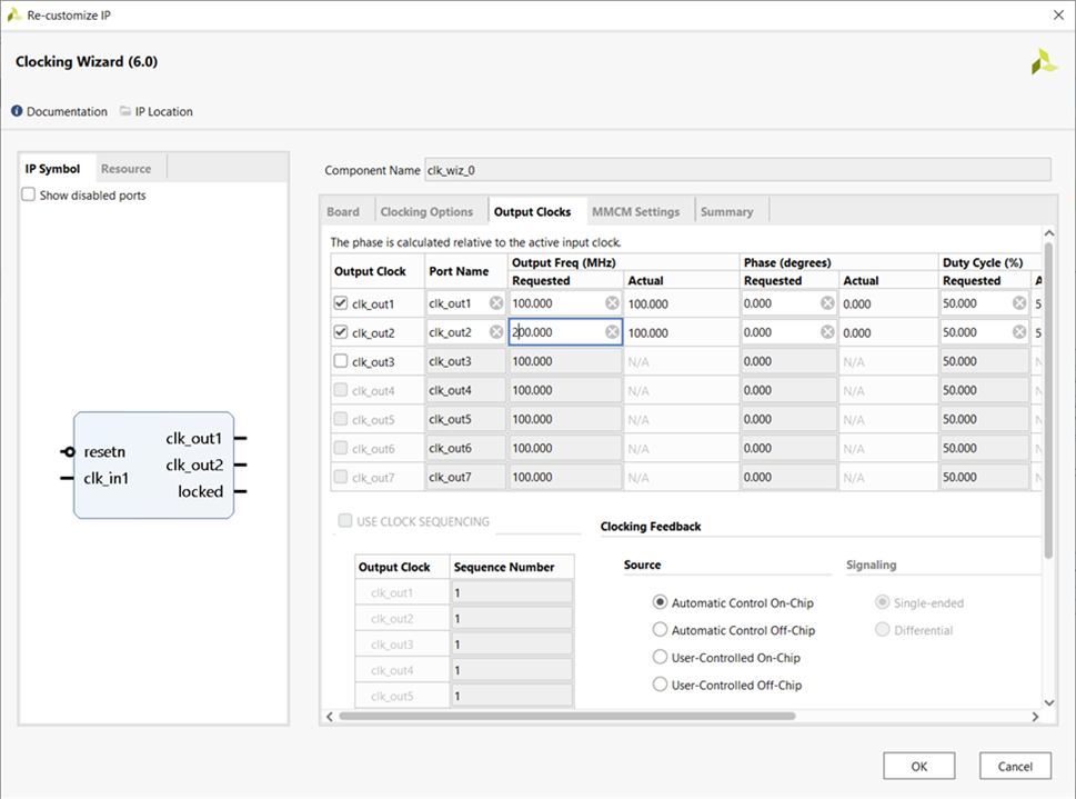
Double click on the 12MHz clocking wizard and generate secondary output clock of 200 MHz.

image

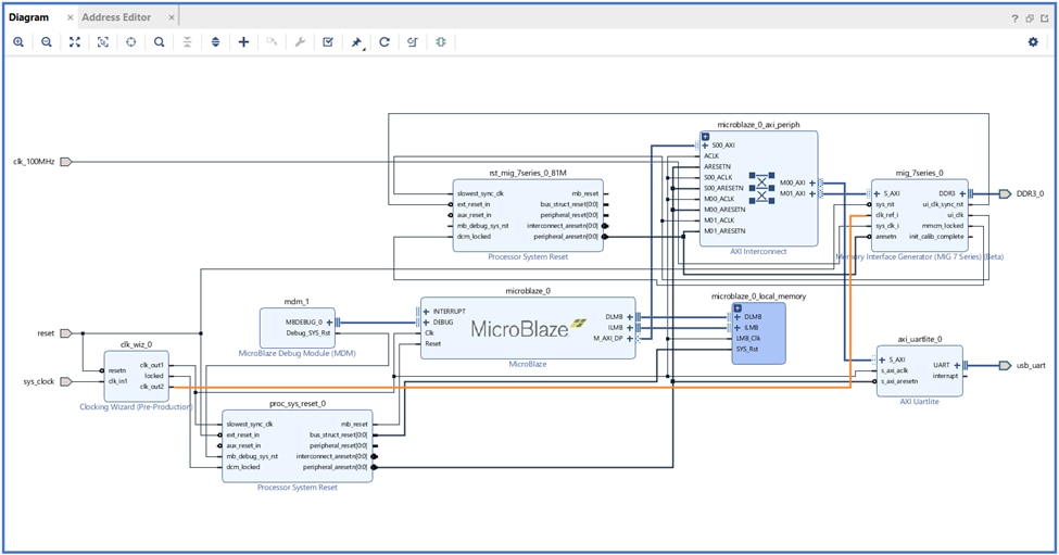
Connect 200MHz clock from clocking wizard to DDR clk_ref_i. The completed block design looks like as shown in the below image.

image

Validate the design and generate the bitstream. Export hardware and launch SDK.

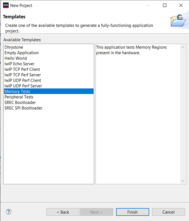
Go to File New Application Project Select the Memory Test application template and build the project.

image

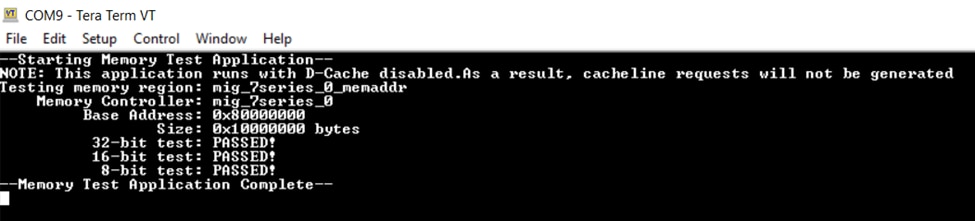
Now program the FPGA and on successfully completing the Memory Test log as shown below will be displayed on the console.

image

The Tcl file of the block design is included in Github Repo.

 Thank you for reading this blog, even though it is a bit lengthy hope I have covered some details on testing DDR on Arty-S7.

References

[1] Xilinx 7 Series MIG User Guide

[2] Arty S7 Reference Manual

  • Sign in to reply
  • Lexou581
    Lexou581 10 months ago in reply to Lexou581

    Ok, so I have done few more test and maybe this can help some people so here is what I found :

    I was launching "Vitis HLS" software to make the example application, but in fact it's "Vitis IDE" that has to be launched. And when I tried to lauch Vitis from Vivado through Tools>Launch Vitis IDE, an error popped, telling me that it can't be launched...

    In fact,  after some researches on the web, it happens that when I installed the design suite (Vivado + Vitis) from the Xilinnx Unified Installer, I chose "Vivado" as the "Product to install", and this include Vitis. But only Vitis HLS (and optionnaly Vitis Model Composer).

    To use Vitis IDE, I needed to uninstall my vivado design suite and reinstall it but this time by selecting "Vitis" as the product to install. And this include Vitis IDE, Vitis HLS and of course the Vivado Design suite !

    All this from a newbie perspective view (never worked before with Vitis) so it is a bit confusing. So if this comment can help other like me...

    • Cancel
    • Vote Up 0 Vote Down
    • Sign in to reply
    • More
    • Cancel
  • Lexou581
    Lexou581 10 months ago

    Thank you for this tutorial, it helps !

    I just have some trouble to run the final stage after having exporting the hardware. When I launch Vitis HLS (2022.1, running on Win10) I don't have the "File>New Application Project" nor I have access to templates...

    All I can have is the option "Clone Examples" in the Vitis welcome page, which gives access to some tutorials, including memory interface ones, but nothing similar to this tutorial so it's a bit confusing (and frustrating as I can't end this tutorial ^^)

    Any idea to make things work ? It seems that I don't use the same version of Vitis but it's the one that was installed with vivado 2022.1.

    • Cancel
    • Vote Up 0 Vote Down
    • Sign in to reply
    • More
    • Cancel
  • hrishi98
    hrishi98 over 1 year ago in reply to saadtiwana_int

    MIG uses IDELAY and ODELAY blocks and this reference clock is used to drive them. This clock can either be generated by MIG itself by adding extra clock similar to ui_clock or can be fed extrenally.

    image

    Refer https://docs.xilinx.com/v/u/1.0-English/ug586_7Series_MIS for further details.

    • Cancel
    • Vote Up 0 Vote Down
    • Sign in to reply
    • More
    • Cancel
  • saadtiwana_int
    saadtiwana_int over 1 year ago

    Thanks for sharing this excellent write up. Topics like these don't get covered often. 

    I want to ask what is the purpose of the Reference clock for the MIG, and what was the reason to connect it to 200Mhz clock. 

    Thanks,
    Saad

    • Cancel
    • Vote Up 0 Vote Down
    • Sign in to reply
    • More
    • Cancel
element14 Community

element14 is the first online community specifically for engineers. Connect with your peers and get expert answers to your questions.

  • Members
  • Learn
  • Technologies
  • Challenges & Projects
  • Products
  • Store
  • About Us
  • Feedback & Support
  • FAQs
  • Terms of Use
  • Privacy Policy
  • Legal and Copyright Notices
  • Sitemap
  • Cookies

An Avnet Company © 2023 Premier Farnell Limited. All Rights Reserved.

Premier Farnell Ltd, registered in England and Wales (no 00876412), registered office: Farnell House, Forge Lane, Leeds LS12 2NE.

ICP 备案号 10220084.

Follow element14

  • X
  • Facebook
  • linkedin
  • YouTube