element14 Community
element14 Community
    Register Log In
  • Site
  • Search
  • Log In Register
  • Community Hub
    Community Hub
    • What's New on element14
    • Feedback and Support
    • Benefits of Membership
    • Personal Blogs
    • Members Area
    • Achievement Levels
  • Learn
    Learn
    • Ask an Expert
    • eBooks
    • element14 presents
    • Learning Center
    • Tech Spotlight
    • STEM Academy
    • Webinars, Training and Events
    • Learning Groups
  • Technologies
    Technologies
    • 3D Printing
    • FPGA
    • Industrial Automation
    • Internet of Things
    • Power & Energy
    • Sensors
    • Technology Groups
  • Challenges & Projects
    Challenges & Projects
    • Design Challenges
    • element14 presents Projects
    • Project14
    • Arduino Projects
    • Raspberry Pi Projects
    • Project Groups
  • Products
    Products
    • Arduino
    • Avnet Boards Community
    • Dev Tools
    • Manufacturers
    • Multicomp Pro
    • Product Groups
    • Raspberry Pi
    • RoadTests & Reviews
  • Store
    Store
    • Visit Your Store
    • Choose another store...
      • Europe
      •  Austria (German)
      •  Belgium (Dutch, French)
      •  Bulgaria (Bulgarian)
      •  Czech Republic (Czech)
      •  Denmark (Danish)
      •  Estonia (Estonian)
      •  Finland (Finnish)
      •  France (French)
      •  Germany (German)
      •  Hungary (Hungarian)
      •  Ireland
      •  Israel
      •  Italy (Italian)
      •  Latvia (Latvian)
      •  
      •  Lithuania (Lithuanian)
      •  Netherlands (Dutch)
      •  Norway (Norwegian)
      •  Poland (Polish)
      •  Portugal (Portuguese)
      •  Romania (Romanian)
      •  Russia (Russian)
      •  Slovakia (Slovak)
      •  Slovenia (Slovenian)
      •  Spain (Spanish)
      •  Sweden (Swedish)
      •  Switzerland(German, French)
      •  Turkey (Turkish)
      •  United Kingdom
      • Asia Pacific
      •  Australia
      •  China
      •  Hong Kong
      •  India
      •  Korea (Korean)
      •  Malaysia
      •  New Zealand
      •  Philippines
      •  Singapore
      •  Taiwan
      •  Thailand (Thai)
      • Americas
      •  Brazil (Portuguese)
      •  Canada
      •  Mexico (Spanish)
      •  United States
      Can't find the country/region you're looking for? Visit our export site or find a local distributor.
  • Translate
  • Profile
  • Settings
FPGA
  • Technologies
  • More
FPGA
Blog FPGA: Waves 2: Simple Sinewave
  • Blog
  • Forum
  • Documents
  • Quiz
  • Events
  • Polls
  • Files
  • Members
  • Mentions
  • Sub-Groups
  • Tags
  • More
  • Cancel
  • New
Join FPGA to participate - click to join for free!
  • Share
  • More
  • Cancel
Group Actions
  • Group RSS
  • More
  • Cancel
Engagement
  • Author Author: jc2048
  • Date Created: 20 Sep 2019 10:09 PM Date Created
  • Views 4103 views
  • Likes 10 likes
  • Comments 7 comments
  • xp2
  • microchip
  • mcp4821
  • experimenting
  • dac
  • brevia2 board
  • fpga
  • vhdl
  • lattice
  • jc2048
Related
Recommended

FPGA: Waves 2: Simple Sinewave

jc2048
jc2048
20 Sep 2019

FPGA: Making Waves


Introduction


I have a small Brevia 2 development board [1] from Lattice Semiconductor featuring one of their XP2-

family FPGAs. I'm using it to explore, in a very simple, basic kind of way, digital signal generation and

processing. I'm using VHDL to describe the digital logic that I'm designing.

In the last blog I described a simple circuit using a low-cost 12-bit SPI DAC from Microchip, an MCP4821.

I tested it by throwing together some VHDL to drive the DAC data with the output of a counter, generating

a simple, linear ramp as a waveform. This time I'm going to have a go at generating a sine wave and, to

fascilitate that, I'll be using one of the block memories on the FPGA as a look-up table.


Since I've not used the Lattice FPGAs before, it will be a useful introduction in to how they handle

their proprietory elements (multipliers, block memories, PLLs, etc) in the Diamond design suite.


Using a Block Memory as a ROM


This particular FPGA has nine EBRs [Embedded Block RAMs]. Each EBR can have its contents initialised at

start-up from the bitstream that configures the FPGA. If the write signal is disabled, the device will

then operate as a ROM [Read-Only Memory] (actually, almost like a ROM: the applications material points

out that the set-up and hold times on the address and other signals need to be observed to avoid

corruption of the contents, which is something to bear in mind).


Design suites need a way of connecting to such components. Previously I'd worked with Xilinx Spartan

devices, using Web ISE as the design environment, and there it can simply be done by instantiating the

component in the VHDL source (starting with a supplied template) and letting the software sort it all out

in the background. With Diamond, it turned out that there is an intermediate step where a utility within

Diamond, called IPExpress, allows primitives like memory elements to be selected and configured, and a

module to be automatically created to include in the project. Once the module is available, the element

can then be simply declared as a component in the VHDL and the connections achieved through an

instantiation statement.


Here's a view of my module in IPExpress:


image


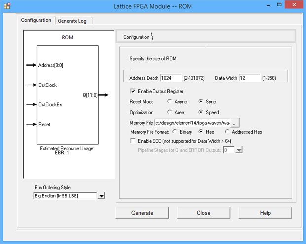
After selecting ROM from the list, putting in a filename for the module and selecting the language (VHDL

in my case), clicking on the customize button brought up this dialog box:


image


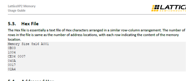
That should have been straightforward too, except that I got an error on loading the Memory File that I'd

generated with a sine table in it. Here's what the Lattice documentation gives for the format:


image


Unfortunately it's wrong. There is no header line and it should just be a list of values, one on each

line. Including the 'Memory Size ...' part in the grey box looks like it was someone messing up the

formatting of the Technical Note. Once I'd puzzled that one out it was all plain sailing.


Trying It Out


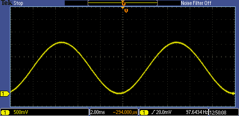
I adapted my original VHDL so that the counter connected to the ROM address lines and the data from the

ROM went to the shift register and this was the nice result from the DAC:


image


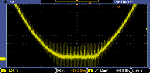
Unfortunately, it's not quite so nice at the lowest point, though I already knew that would be the case

from doing the last blog.


image


Here the sine shape is compromised by the way the op-amp buffer in the DAC behaves near ground. Not only

does it limit the lowest value, distorting the shape of the waveform, but also it seems to take its time

lifting off again and the noise rejection seems much poorer (the 'scope is set to a one second

persistence time).


The Code


Here's the VHDL


------------------------------------------------------------------
--     ***** Waves_Sine *****       --
--  Test of MCP4821 DAC with sine wave from look-up table       --
------------------------------------------------------------------
-- JC 20th September 2019          --
------------------------------------------------------------------
-- Rev    Date         Comments         --
-- 01     20-Sept-2019            --
------------------------------------------------------------------
library ieee;
use ieee.std_logic_1164.all;
use ieee.std_logic_arith.all;
use ieee.std_logic_unsigned.all;
entity wave_test_con is port(
  clk_in:   in std_logic;        --- system clock in (50 MHz oscillator)
  --- DAC connections
  mcp4821_ncs: out std_logic;        --- DAC cs
  mcp4821_sck: out std_logic;        --- DAC sck
  mcp4821_sdi: out std_logic;        --- DAC sdi
  mcp4821_nldac: out std_logic;        --- DAC load
  --- misc control signals on evaluation board that it might be good to hold at fixed levels
  spi_cs:   out std_logic;        --- 
  hold_n:   out std_logic;        --- 
  sram_cen:  out std_logic;        --- 
  sram_oen:  out std_logic;        --- 
  sram_wen:  out std_logic;        --- 
  uart_tx:  out std_logic);        --- 
 
end wave_test_con;
architecture arch_wave_test of wave_test_con is
signal spi_send, spi_ncs, spi_ncs_del: std_logic;
signal waveform_count: std_logic_vector (11 downto 0);
signal spi_output_sr_bit_count: std_logic_vector (5 downto 0);
signal spi_output_sr: std_logic_vector (15 downto 0);
signal interval_count: std_logic_vector (8 downto 0);
signal sine_value: std_logic_vector (12 downto 0);
component sine_rom
    port (
        Address: in  std_logic_vector(9 downto 0); 
        OutClock: in  std_logic; 
        OutClockEn: in  std_logic; 
        Reset: in  std_logic; 
        Q: out  std_logic_vector(11 downto 0));
 end component;
begin
 wave_test_stuff: process (clk_in)
  begin
  
   if (clk_in'event and clk_in='1') then
  
    --- interval_count counts at the clock rate (50MHz)
    --- counts down by 500, so spi_send occurs every 10us (100kHz)
    if (interval_count(8 downto 0) = b"000000000") then     --- if zero
     interval_count(8 downto 0) <= b"111110011";      --- preset to 499
     spi_send <= '1';
    else
     interval_count(8 downto 0) <= interval_count(8 downto 0) - 1; --- count down
     spi_send <= '0';
    end if;
    --- spi ncs goes low when triggered by spi_send, goes hi again when bitcount reaches 31
    
    if (spi_send = '1') then
     spi_ncs <= '0';
    elsif (spi_output_sr_bit_count(5 downto 0) = b"111111") then
     spi_ncs <= '1';
    end if;
    
    spi_ncs_del <= spi_ncs;
    --- spi output bit count only counts when enable spi cs is low
    
    if (spi_ncs = '0') then
     spi_output_sr_bit_count(5 downto 0) <= spi_output_sr_bit_count(5 downto 0) + 1;
    else
     spi_output_sr_bit_count(5 downto 0) <= b"000000";
    end if;
    
    --- waveform count - this in now going to be the address for the look-up table
    
    if (spi_send = '1') then
     waveform_count(11 downto 0) <= waveform_count(11 downto 0) + 1;
    end if;
    --- spi output shift register
    
    if (spi_send = '1') then             --- load...
     spi_output_sr(11 downto 0) <= sine_value(11 downto 0);     ---   dac data from look-up table
     spi_output_sr(15 downto 12) <= b"0011";         ---   dac control bits
    elsif (spi_ncs = '0' and spi_output_sr_bit_count(1 downto 0) = b"11") then --- shift...
     spi_output_sr(15 downto 1) <= spi_output_sr(14 downto 0);    ---  the register contents
     spi_output_sr(0) <= '0';
    end if;
   end if;
  
   ---
   
   mcp4821_ncs <= spi_ncs;
   mcp4821_sck <= spi_output_sr_bit_count(1);
   mcp4821_sdi <= spi_output_sr(15);
   mcp4821_nldac <= '0';
  
   --- hold these device control pins at a fixed level to stop them flapping around
   spi_cs <= '1';
   hold_n <= '1';
   sram_cen <= '1';
   sram_oen <= '1';
   sram_wen <= '1';
   uart_tx <= '1';
  end process wave_test_stuff;
 
  
  sine_rom1: sine_rom
   port map(Address => waveform_count(9 downto 0), OutClock => clk_in, OutClockEn => '1', Reset => '0', Q => sine_value(11 downto 0));
end arch_wave_test;


and here's the simple C program I used to generate the sine values for the memory initialisation file


/****************************************************************/
/* sintab.c                                                     */
/*           Data values for sine look-up table                 */
/*           for Lattice FPGA ROM initialisation                */
/*           Output file is called sineTable.mem                */
/*           13th April 2018    Jon Clift                       */
/*--------------------------------------------------------------*/
/* Rev   Date       Comments                                    */
/* 1.0   18/09/2019                                             */
/****************************************************************/
#include <stdio.h>
#include <conio.h>
#include <string.h>
#include <dos.h>
#include <errno.h>
#include <math.h>
// variables
FILE *handle;
char temp_string[256];
unsigned int sineTable[1024];
// main routine
void main(int argc,char *argv[])
{   int i,j;
    /* print banner */
    printf("\n--- sinetab DOS utility program V1.0 ---\n");
    printf("Builds sine table for Lattice FPGA ROM.\n");
 
    /* generate sine table in array */
   for(i=0;i<1024;i++) {
        sineTable[i]=(unsigned int) (((sin((2 * 3.1415926/1024)*i)) * 2048) + 2048);
        }
     /* open output file */
    if((handle=fopen("sinetab.mem","wt"))==NULL) {
        printf("Failed to open output file.\n");
        _fcloseall();
        }
 else {
  /* write header */
//  fprintf(handle,"// Auto-generated by memint 09/19/2019 16:41:21\n");
//  fprintf(handle,"#Format=Hex\n");
//  fprintf(handle,"#Depth=512\n");
//  fprintf(handle,"#Width=12\n");
//  fprintf(handle,"#AddrRadix=3\n");
//  fprintf(handle,"#DataRadix=3\n");
//  fprintf(handle,"#Data\n");
     /* write table to file */
  for (i=0;i<1024;i++) {
   fprintf(handle,"%03X\n",sineTable[i]);
   }
  
  /* close output file */
  fclose(handle);
     printf("Done.\n");
  }
 
}


Note that the values are unsigned binary in a form suitable for throwing directly at the DAC. Later I'll

probably move to a better representation for doing arithmetic with.


I now need to think what I go on and do with my new-found capability to generate and manipulate sine

waves.


If you found this interesting and would like to see more blogs I've written, a list can be found here: jc2048 Blog Index


[1] http://www.latticesemi.com/en/Products/DevelopmentBoardsAndKits/LatticeXP2Brevia2DevelopmentKit.aspx

  • Sign in to reply

Top Comments

  • michaelkellett
    michaelkellett over 5 years ago +6
    Now you've done it the hard way - try the other way: https://forums.xilinx.com/t5/DSP-IP-and-Tools/Generating-SIne-Wave/td-p/53120 (scroll all the way down to Eilert's reply where you'll find this gem…
  • neuromodulator
    neuromodulator over 5 years ago +4
    Taking advantage of the symmetry of sin/cos, and through interpolation you could significantly reduce the LUT size. Alternatively you could also use CORDIC.
  • michaelkellett
    michaelkellett over 5 years ago in reply to jc2048 +4
    You are right re. the numerical error. You can use IPexpress to generate signed or unsigned multipliers of arbitrary size - it will add pipelining (avoid at first) and use more than one multiplier to get…
  • jc2048
    jc2048 over 5 years ago in reply to jc2048

    This is work in progress, but I found a little time to try the computed oscillator and it seems to do something.


    image


    No reconstruction filter. I'm stopping and restarting it during the periods when the output is flat. Haven't looked at whether it will run continuously yet. Hopefully it will look sine-like when it's filtered.


    Frequency and amplitude aren't what I intended. I was trying for 5kHz but seem to have ended up with 20kHz, or something like that. The amplitude is about half what I intended. [The flat section is at the halfway point on the DAC range - scope channel has a 1.024V offset on it.]


    Took me a while to realise that it's basically a model of simple harmonic motion. Major disadvantage with it would be trying to change the frequency on the fly [because of the stored history].

    • Cancel
    • Vote Up +2 Vote Down
    • Sign in to reply
    • More
    • Cancel
  • neuromodulator
    neuromodulator over 5 years ago in reply to jc2048

    I implemented a Sin Cos using a lut from 0 to pi, and linear interpolation. Dunno VHDL, but at least in Xilinx's Verilog I was able to implement the LUT generation in Verilog itself. Doing half of the LUT is very straightforward, basically you just use the MSB as a sign bit. I did some simulation in python and cubic interpolation generated negligible errors (around 1e-6 if my memory serves me well) with very few LUT elements (64).

    • Cancel
    • Vote Up +2 Vote Down
    • Sign in to reply
    • More
    • Cancel
  • jc2048
    jc2048 over 5 years ago in reply to neuromodulator

    Thanks for the suggestions.


    For the moment, I think I'll stick with using a complete cycle in the look-up table for simplicity, but I do take your point that using symmetry would be a way of increasing the phase resolution by a factor of either two or four.


    The CORDIC stuff was fascinating to read about - it's not something I'm familiar with at all. Wikipedia have a good page on the history which I've just been reading. Yet more good material to experiment with if I ever find the time (I'll add it to the list).

    • Cancel
    • Vote Up +2 Vote Down
    • Sign in to reply
    • More
    • Cancel
  • michaelkellett
    michaelkellett over 5 years ago in reply to jc2048

    You are right re. the numerical error.


    You can use IPexpress to generate signed or unsigned multipliers of arbitrary size - it will add pipelining (avoid at first) and use more than one multiplier to get what you need.


    When you get going a really good challenge is to make a sine wave generator with a log frequency sweep - I did it on a Lattice ECP3, using Lattice's CORDIC IP (paid for image) but my sweeping code,


    at 256k samples per second I needed 128 bit arithmetic to cope with a 1000 second sweep, the problem is that you need a frequency update every sample - you might run out of hardware multipliers on the

    small XP2 on the Brevia board - although you can be clever and do a lot of multiplies every sample with just one multiplier since they are quite fast.


    MK

    • Cancel
    • Vote Up +4 Vote Down
    • Sign in to reply
    • More
    • Cancel
  • neuromodulator
    neuromodulator over 5 years ago

    Taking advantage of the symmetry of sin/cos, and through interpolation you could significantly reduce the LUT size. Alternatively you could also use CORDIC.

    • Cancel
    • Vote Up +4 Vote Down
    • Sign in to reply
    • More
    • Cancel
>
element14 Community

element14 is the first online community specifically for engineers. Connect with your peers and get expert answers to your questions.

  • Members
  • Learn
  • Technologies
  • Challenges & Projects
  • Products
  • Store
  • About Us
  • Feedback & Support
  • FAQs
  • Terms of Use
  • Privacy Policy
  • Legal and Copyright Notices
  • Sitemap
  • Cookies

An Avnet Company © 2025 Premier Farnell Limited. All Rights Reserved.

Premier Farnell Ltd, registered in England and Wales (no 00876412), registered office: Farnell House, Forge Lane, Leeds LS12 2NE.

ICP 备案号 10220084.

Follow element14

  • X
  • Facebook
  • linkedin
  • YouTube