


Introduction:
The Arty S7 contains a 256MB DDR3L SDRAM with a 16-bit bus. For proper operation of the memory, a memory controller and physical layer (PHY) interface needs to be included in the FPGA design. The easiest way to accomplish this on the Arty S7 is to use the Xilinx 7-series memory interface solutions core generated by the MIG (Memory Interface Generator) Wizard. The MIG Wizard can generate a native FIFO-style or an AXI4 interface to connect to user logic. Read more here.
In this blog, we will try to include this memory in our design and interact with it. Instead of using BRAM as data and instruction memory, we will try to use the SDRAM.
If you are new to FPGA or you haven't yet created your first project on the board, I will recommend you to go through the below mentioned blogs first:
Creating Block Design:
- Open Vivado and create a new RTL project.
- Click on "Create Block Design".
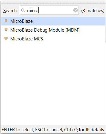
- Add a MicroBlaze IP.
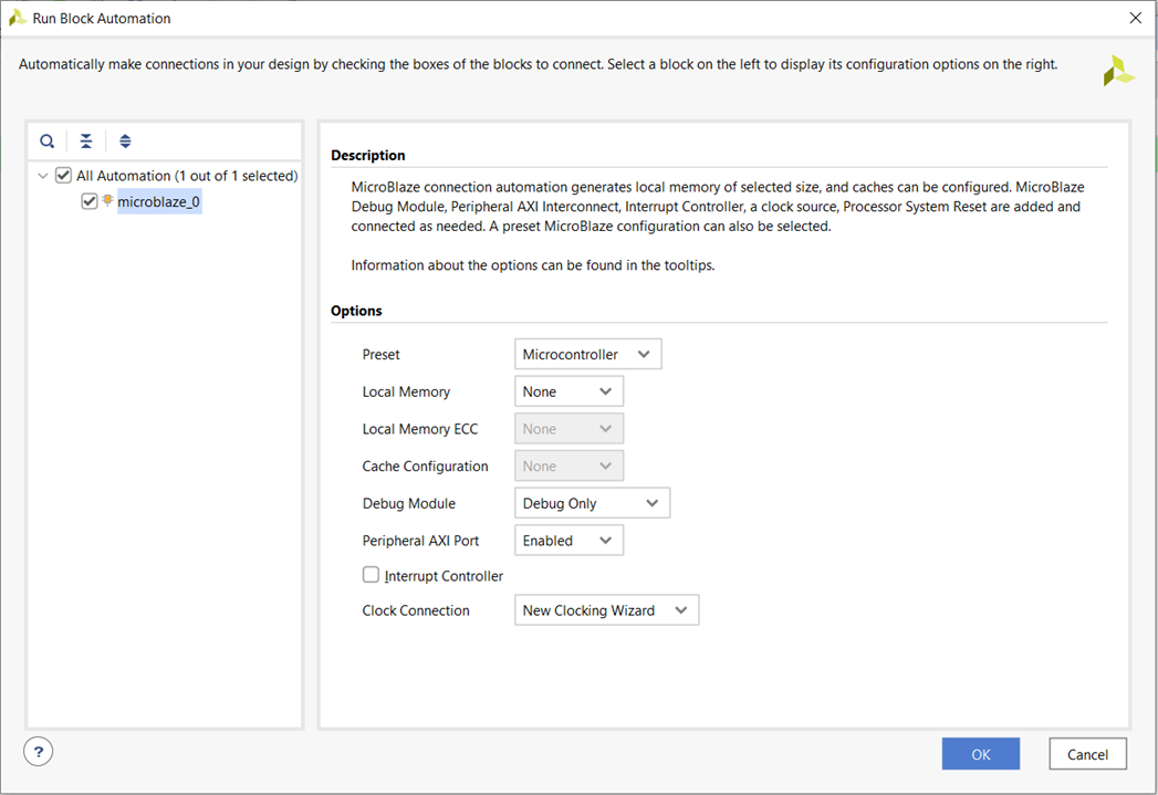
- Run Block Automation. Select the settings as shown below. Note that we don't need BRAM because we will be using the SDRAM instead of the BRAM. Click on "OK".
- Open the Clocking Wizard by double clicking on it and select "Active Low" for "Reset Type".
- Drag and drop the "System Clock" from the "Board" Tab into our design (it should get connected to the clocking wizard).
- Now run connection automation by selecting all automation.
- Now add a UARTlite IP and again run connection automation by selecting all automation.
- You can now regenerate the layout.
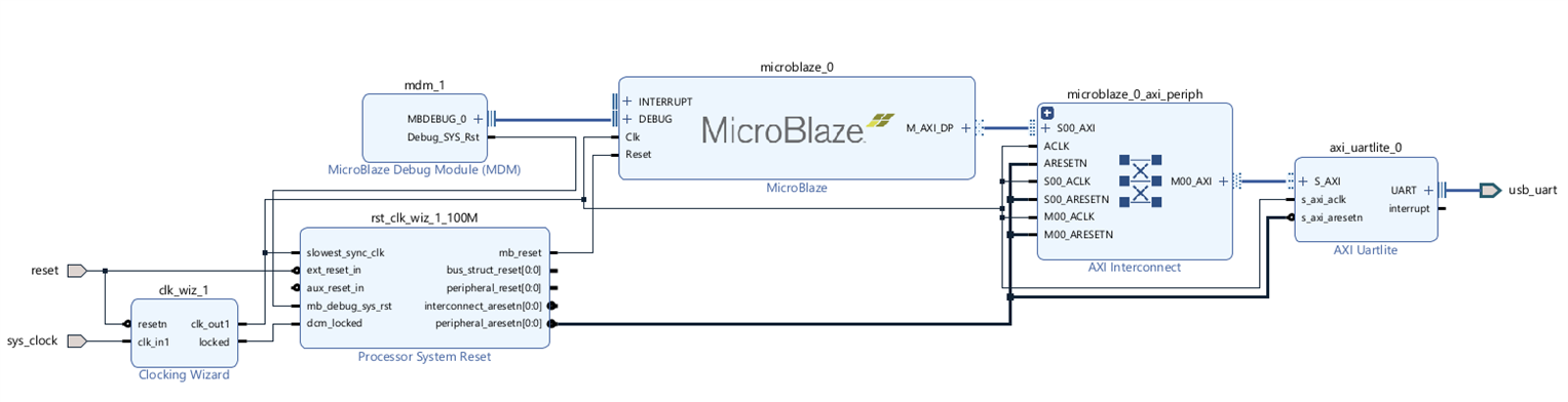
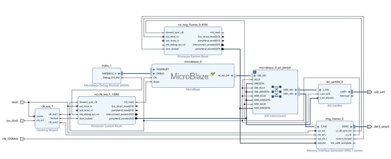
- Your design should look something like this:
- Now, we need to add the "DDR3 SDRAM" to our design.
- Go to the "Board" tab and drag and drop "DDR3 SDRAM" to our design from there.
- Now you will see that a "Memory Interface Generator" block with "DDR3 SDRAM" as an external port will be added to your design.
- Now, double click on the MIG block to customize it.
- Actually, majority of the settings will be already selected according to our SDRAM. But still we should go through it just to confirm it.
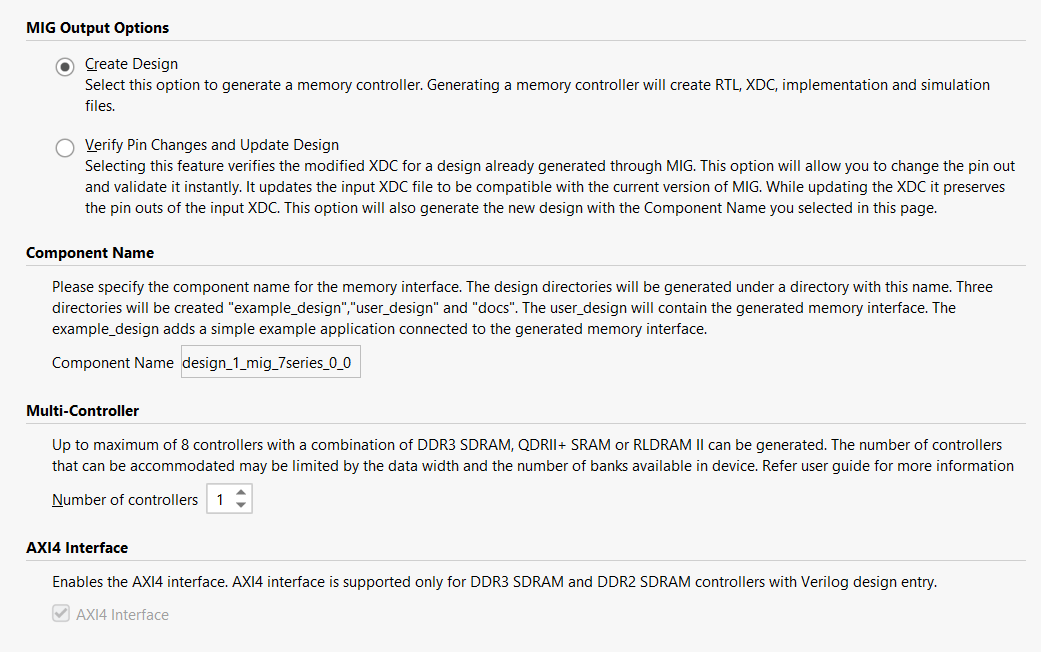
- In the "MIG Output Options", "Create Design" should be selected. Click on "Next".
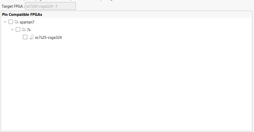
- Leave the "Pin Compatible FPGAs" as it is. Click on "Next".
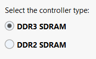
- Select "DDR3 SDRAM" for controller type. Click on "Next".
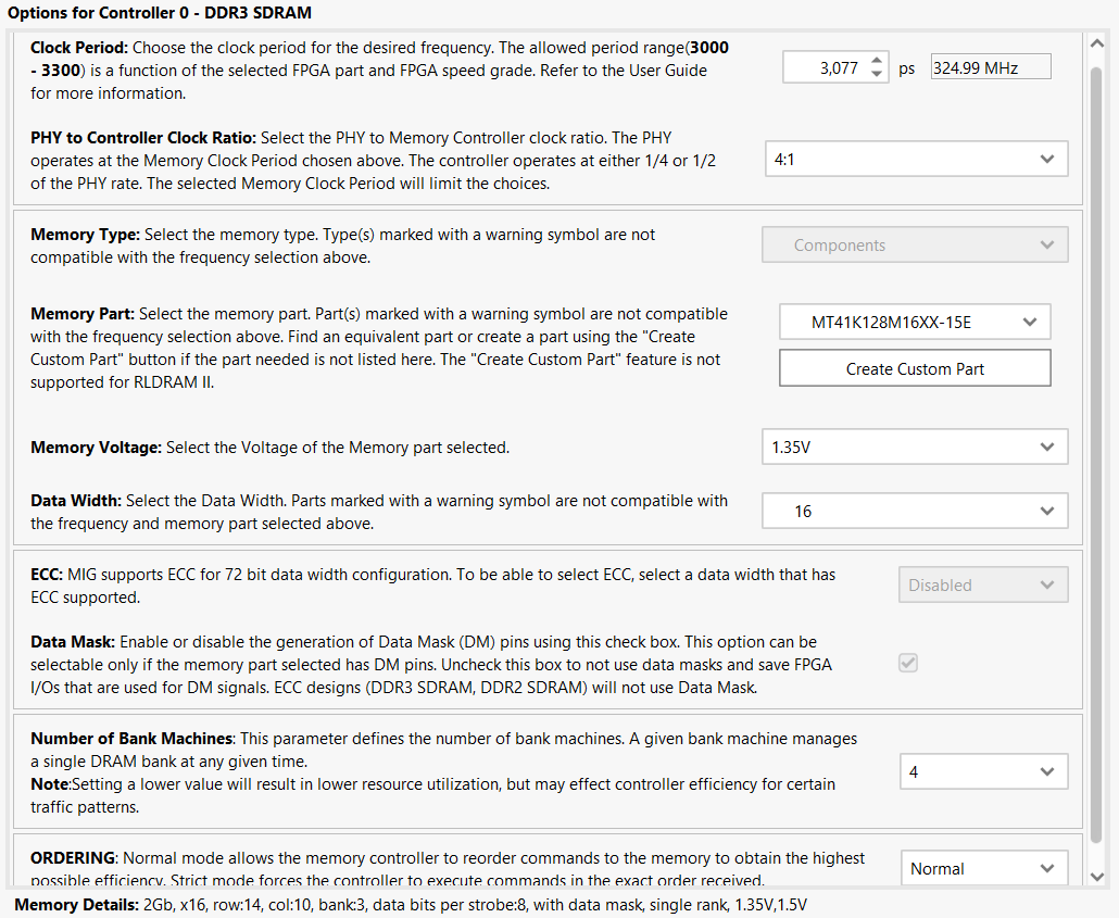
- Check the following settings for "Options for Controller 0". Click on "Next".
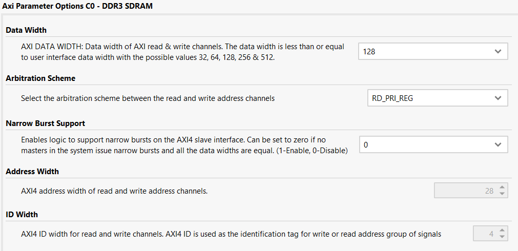
- Leave the "AXI Parameter Options C0" as it is. Click on "Next".
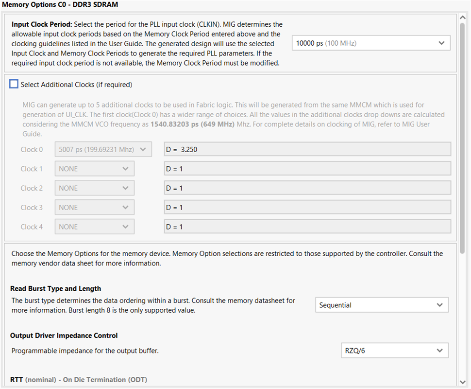
- Check the following options for "Memory Options C0". You can unselect "Select Additional Clocks", we don't need it. Click on "Next".
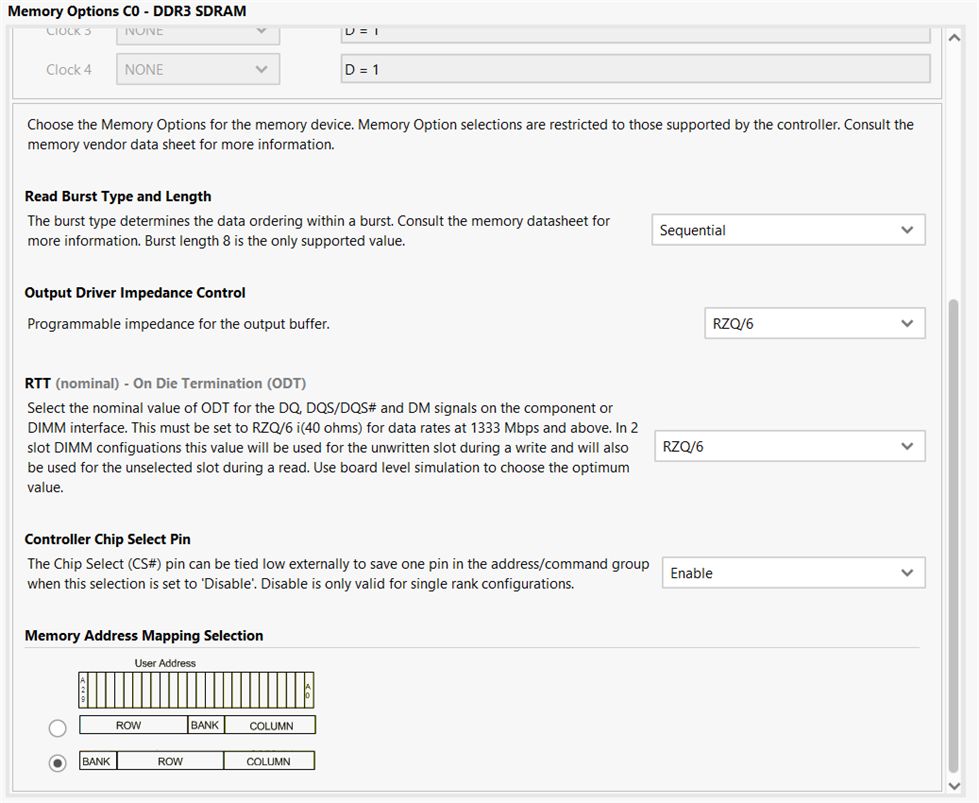
- Check the following settings. Click on "Next".
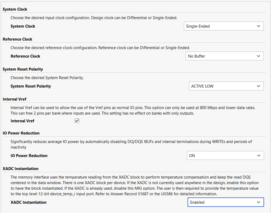
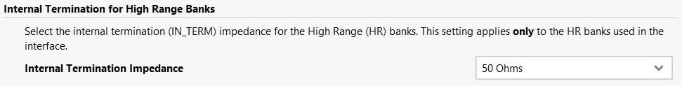
- Select 50 Ohms for "Internal Termination for High Range Banks".
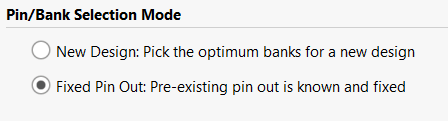
- Select "Fixed Pin Out" for "Pin Selection Mode".
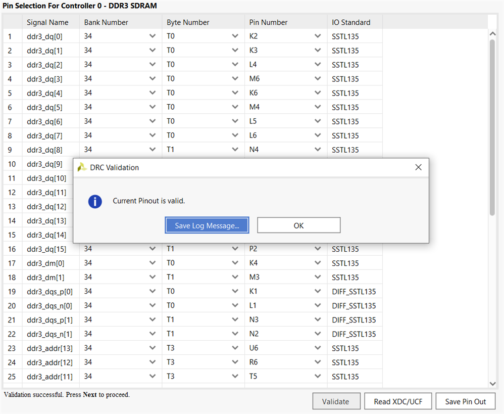
- Click on "Validate" to verify the Pinout.
- Now, keep clicking on "Next", accept the agreement then click on "Generate".
- Now, in the block design, select "clk_ref_i" and "sys_clk_i" and delete them.
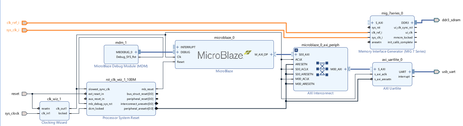
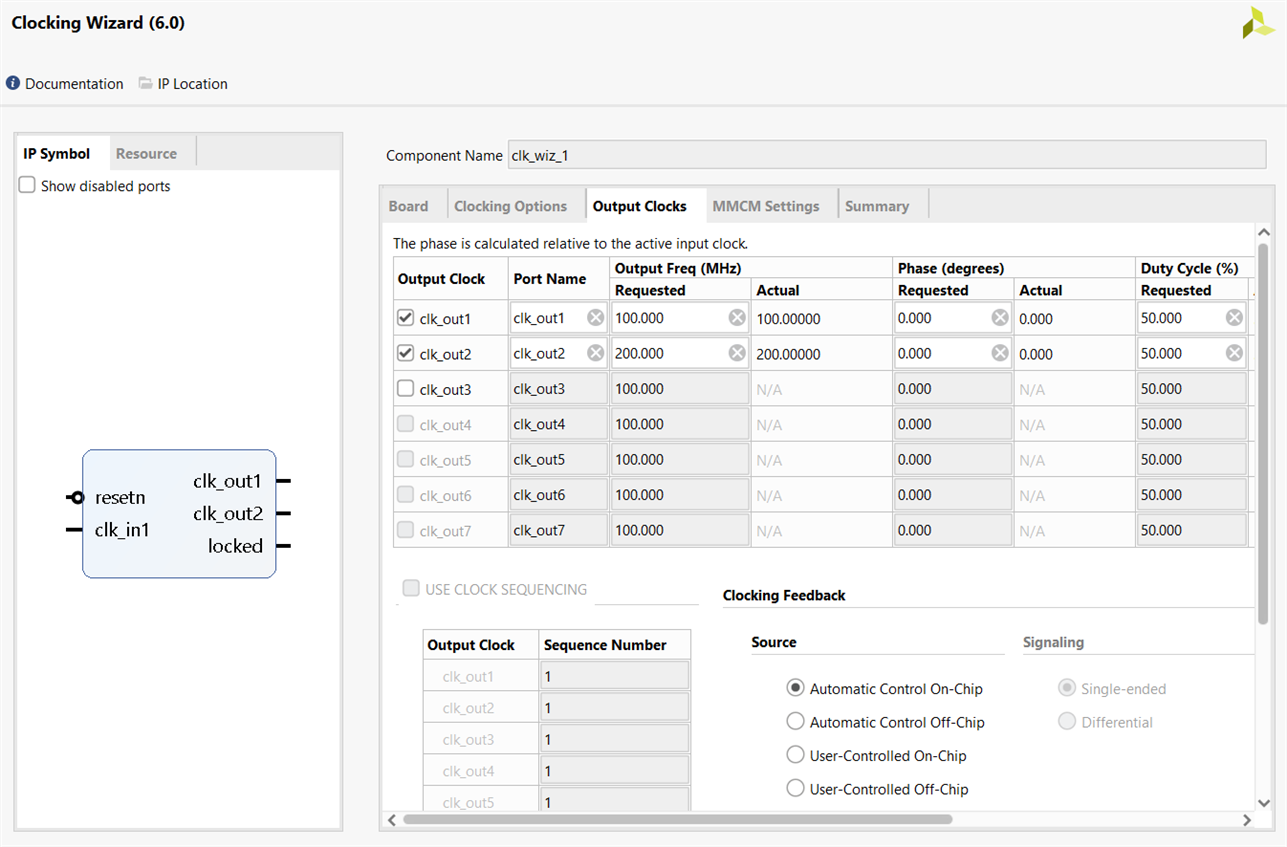
- Now, open the "Clocking Wizard". Go to "Output Clocks", enable "clk_out2" with 200MHz frequency. Click on "OK"
- Connect the "clk_out2" to the "clk_ref_i" port of MIG.
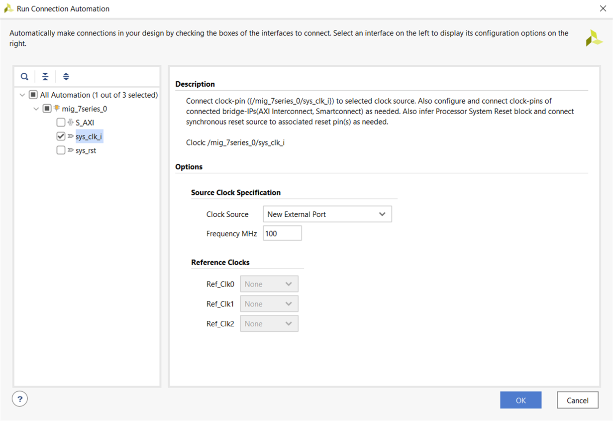
- Click on "Run Connection Automation". Select "sys_clk_i". Select "New External Port" with 100 MHz for "Clock Source". Click on "OK".
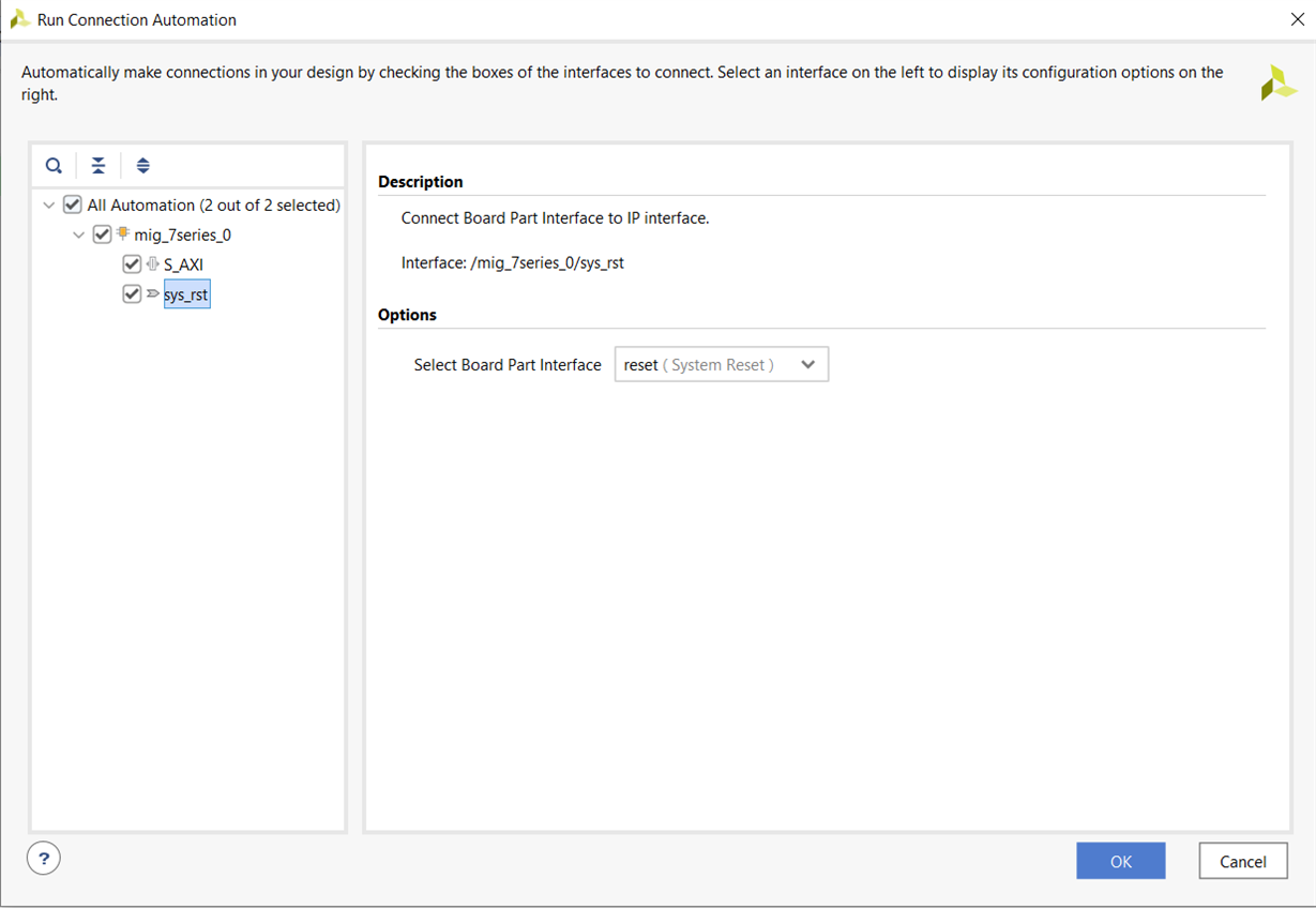
- Now, again run connection automation, select "All Automation". "reset (System Reset)" should be selected for "Select Board Part Interface". Click on "OK".
- You can regenerate the layout now.
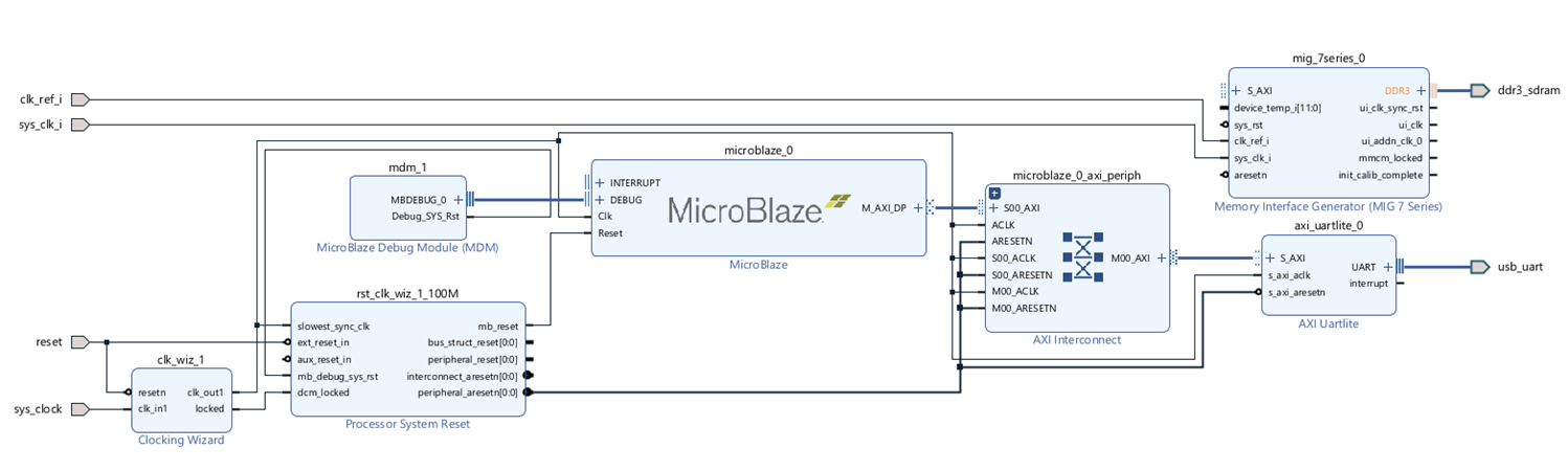
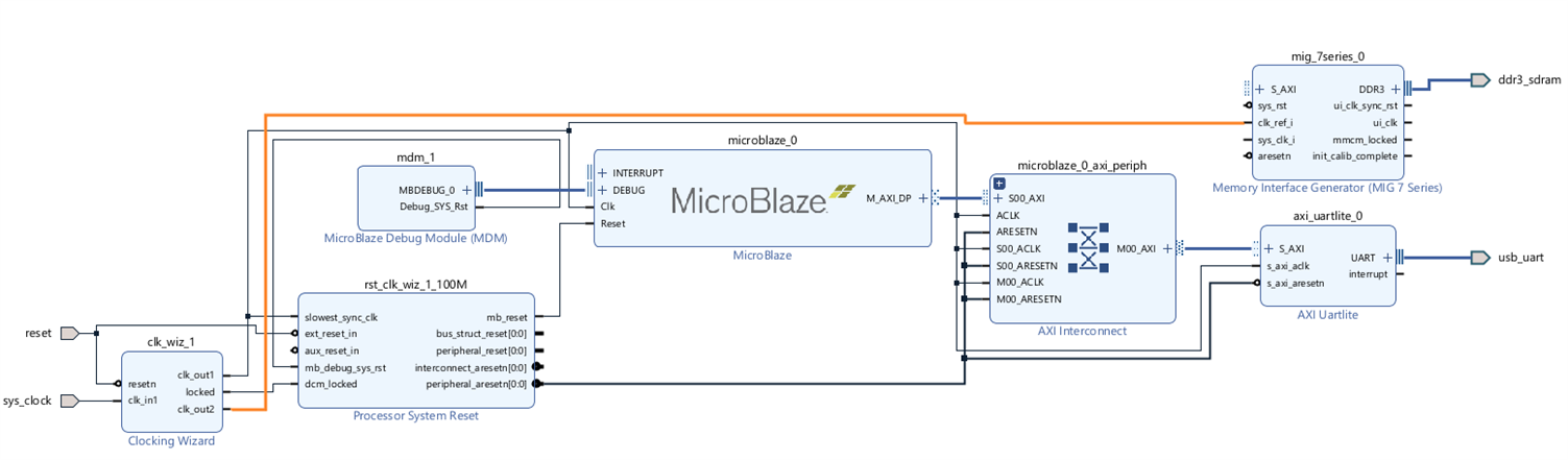
- Now, if you would look at our block design, you will notice that we have a path between MicroBlaze and MIG for data ( i.e. "M_AXI_DP") but we don't have an instruction path. Without it we wouldn't be able to run C code on our design.
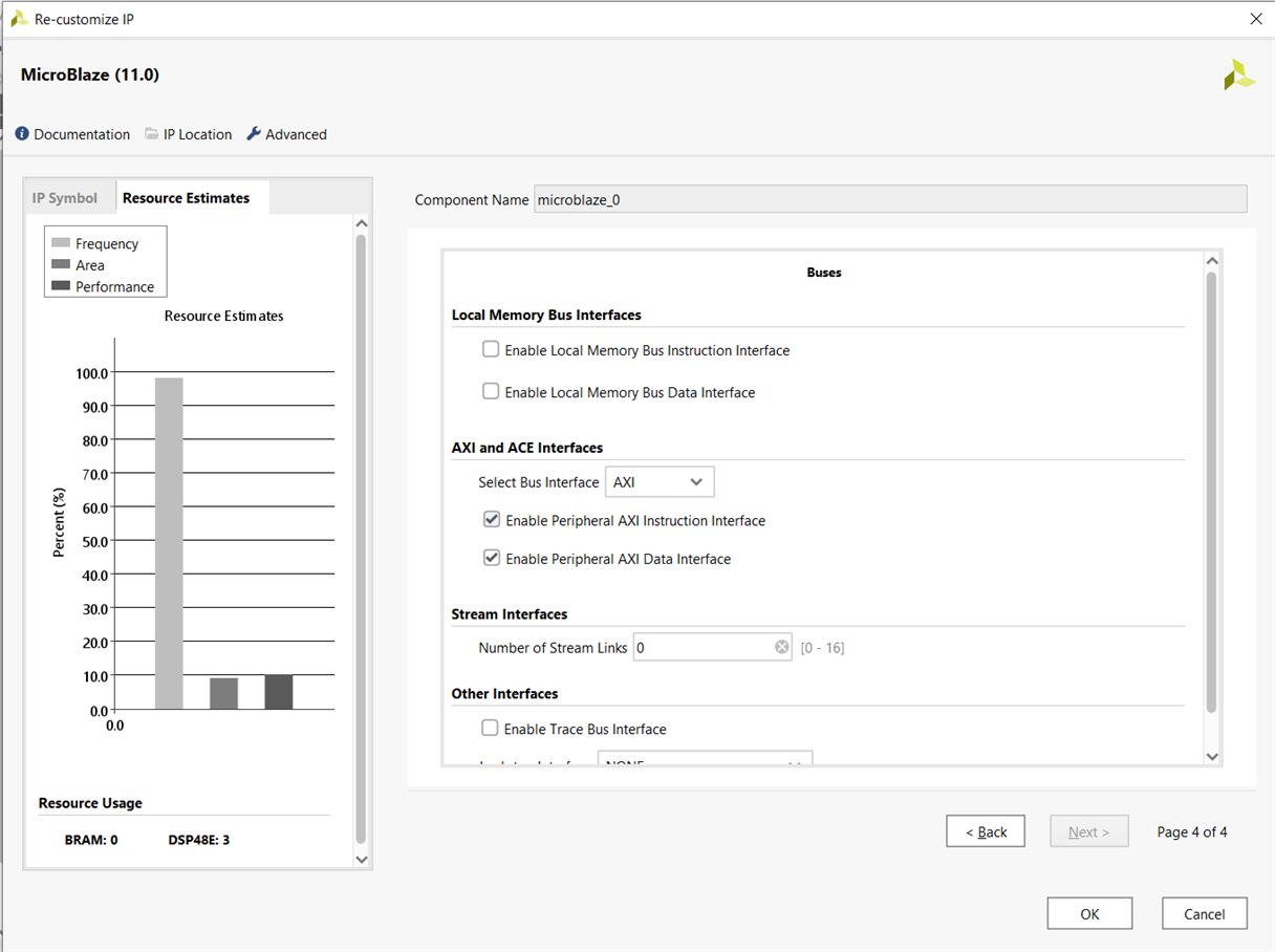
- To enable instruction path, double click on the MicroBlaze IP, go to the 4th page and select "Enable Peripheral AXI Instruction Interface". Click on "OK".
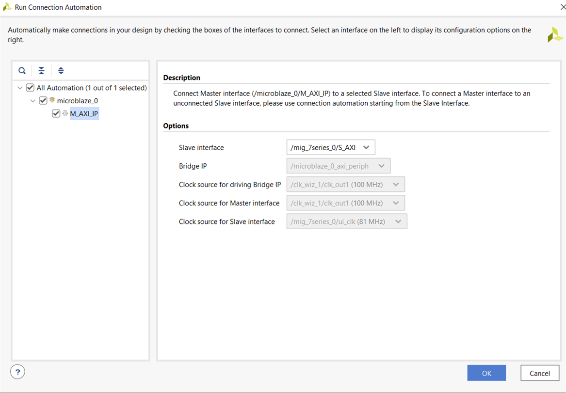
- Now, run connection automation. Select "/mig_7series_0/S_AXI" for "Slave Interface". Click on "OK".
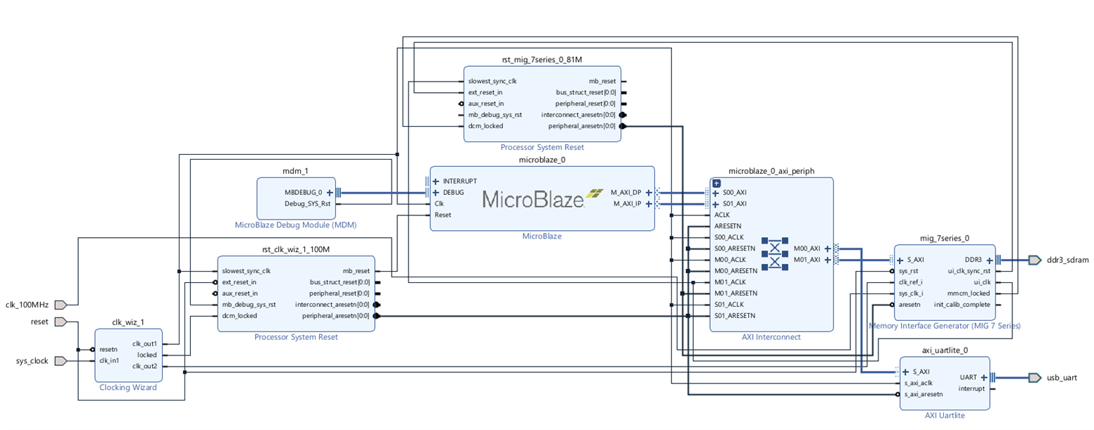
- Regenerate Layout.
- Validate your design.

- Now save your design.
- Create HDL Wrapper for your design, Run Synthesis, Run Implementation and Generate Bitstream.
- It will give you a critical warning after running implementation and the BMM file will not be generated. That is because we don't have BRAM in our design. For now we can proceed without worrying about it.
- Export your hardware and then launch Vitis.
Testing the design:
- Launch your Vitis Workspace. Create an empty C Application project. Select the xsa file that we earlier exported as our platform.
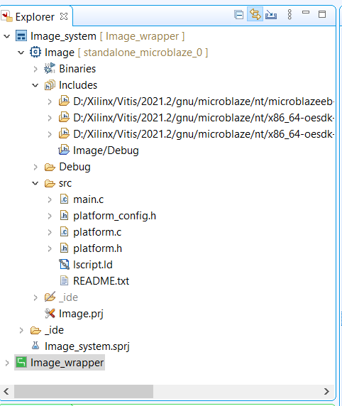
- Create a C language source file inside the "src" folder.
- Copy the code inside the source file:
#include "platform.h" #include "xparameters.h" #include "xil_printf.h" #include "xil_io.h" int main() { init_platform(); int x = 56; int num; Xil_Out8(XPAR_MIG7SERIES_0_BASEADDR + 3, 23); num = Xil_In8(XPAR_MIG7SERIES_0_BASEADDR + 3); xil_printf("%d %d", x, num); cleanup_platform(); return 0; } - We can directly write to a memory location if we know its address. The BASE address and HIGH address for the SDRAM is listed in the "xparameters.h" file. "XPAR_MIG7SERIES_0_BASEADDR" refers to the base address of SDRAM as is given the "xparameters.h" header file.
- The Xil_Out8() function is used to write one byte of data to the memory location specified.
- The Xil_In8() function retrieves one byte data from the memory location specified.
- These functions are defined under the "xil_io.h" header file.
- To know more about these functions, refer this documentation.
- If you will look at our code, you will notice that we have included some header files in our code. The header files "xparameters.h", " xil_printf.h" and "xil_io.h" are already present in the "includes" folder inside the design wrapper folder.
- We need to get the "platform.h" header file. To get it, just create a new Application Project by selecting the "Hello World" template. Inside the "src" folder, you will find three files: "platform_config.h", "platform.h" and "platform.c". Just copy these files to your original project "src" folder. You can now delete the Hello World project. We don't need it now.
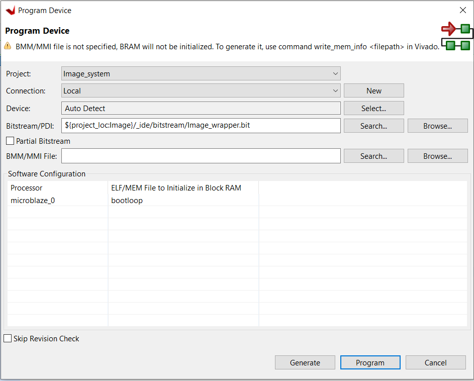
- Connect your board. Notice that there is no BMM file in our project that is because we haven't included BRAM in our design. Program your device.
- Open a Serial Terminal.
- Build your code and then run it on the hardware.
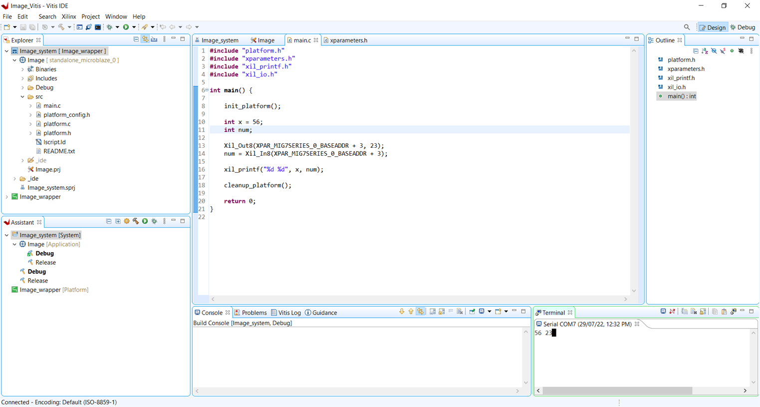
- As it can be seen on the terminal, we have created a variable and accessed its value successfully and we were also able to write directly to a memory location using the Xil_Out8() function. I would like to advice that if your code consists of assigning to and accessing values from a variable then avoid using direct memory location access using Xil_Out because it might overwrite your already existing variable data.
Conclusion:
The IP integrator has made it really easy to customize any design according to our needs. But one will require a little bit of patience and practice to learn to implement correct approach to build their designs and not get confused by seeing vast number of options and features offered by the Vivado Design Suite.