


FPGA gets its power from the flexibility. The design process can be time-consuming but you can design basically anything. In this project, I will give some examples of the multiplication and flexibility of FPGAs.
Multiplication consumes time and sometimes they specify the whole performance of the system. Impulse response or Fourier transform of the discrete signal is calculated by multiplying and adding the massive number of samples because of that the power of the digital signal processor(DSP) chips are compared with their multiplication and addition (MAC) numbers in a second. FPGAs, which provides custom solutions, are used in many applications which require huge MAC operations like military radar applications, adaptive noise cancellations, machine vision, HDTV and etc. The multiplication operation can be performed in many ways on FPGA. Based on the application, it can be implemented parallel or pipelined where the speed is important or it can be implemented to cost small footprint.
The DE0-Nano device 149 configurable pins therefor I will use 32*32 multiplier for the test. You can have more bits to multiply but you can't assign them to the pins. Hence, this is the demonstration of different methodologies, I don't use any other design than the multiplier.
Altera Megafunction
Let's start with the easiest way of multiplication using the libraries  Altera has something called Megafunctions and it is stated like:
As design complexities increase, use of vendor-specific intellectual property (IP) blocks has become a common design methodology. Altera provides parameterizable megafunctions that are optimized for Altera device architectures. Using megafunctions instead of coding your own logic saves valuable design time. Additionally, the Altera-provided functions may offer more efficient logic synthesis and device implementation. You can scale the megafunction’s size by setting parameters.
The Code:
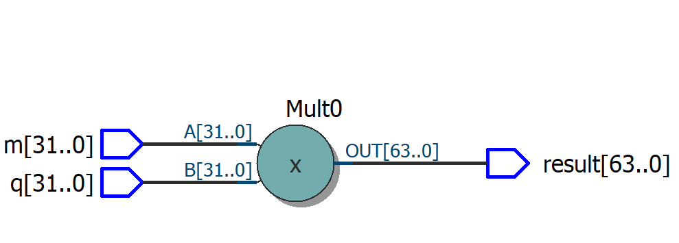
module multiplier(m,q,result);

  input [31:0]m;
  input [31:0]q;
  output [63:0]result;

  assign result = m * q;

endmodule
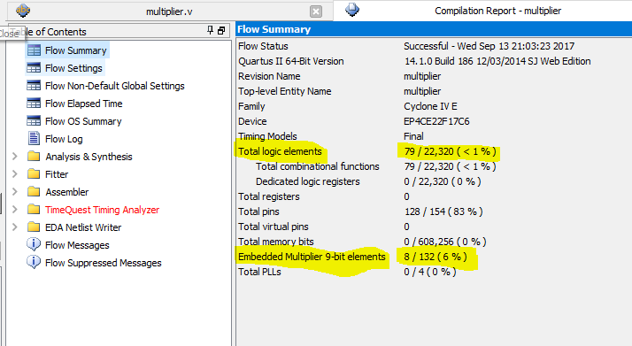
The Result:
RTL Viewer:
It looks like the Altera EP4CE22F17C6 has built-in hardware multipliers and if use "a * b" it is automatically done by the dedicated multiplier. The multiplication is done by using lpm_mult megafunction. It only uses 79 logic elements. It looks like Altera megafunctions are working as expected. They save time and create an efficient logic synthesis. * b
The lpm_mult megafunction can be implemented using either logic resources or dedicated multiplier circuitry in Altera devices. Typically, the lpm_mult megafunction is translated to the dedicated multiplier circuitry when it is available because it provides better performance and resource utilization.
Array Multiplier
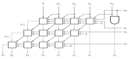
Another design method is array multiplier. Multiplier m and multiplicand q are multiplied by using array multiplier as shown in Figure Array Multiplier which is same as the paper and pencil multiplication. Summands are calculated by multiplying m with each bit of the q by BasePPI module at the top layer and PPI modules in other layers. In order to make the code more readable n-bit BasePPI and PPI modules are used and n-1 layer is generated with a loop. The size of the design is controlled by parameters n.
Array Multiplier
The Code:
module multiplier (m, q, result);


parameter n=32;
//assign inputs and outputs
input [n-1:0] m, q;
output  [2*n-1:0] result;


and(result[0],m[0],q[0]);


wire [n-1:0]link[n-1];


genvar i;
generate
for(i=0;i<n-1;i=i+1)
begin:layers
if(i==0)
BasePPI(m,q[1:0],link[i],result[i+1]);
else
PPI(link[i-1], m, q[i+1] , link[i], result[i+1]);
end
assign result[2*n-1:n]=link[n-2];
endgenerate


endmodule


//****************************************************
//higher tier adder cell instantiating full adder


module PPI(PPI_bit, m, q, ,out,px);


//assign inputs and outputs
parameter n=4;
input [n-1:0] PPI_bit, m;
input q;
output [n-1:0]out;
output  px;


genvar i;
generate


wire [n-1:0]link;

for(i=0;i<n;i=i+1)
begin:PPILayers
if(i==0)
half_adder( (q & m[i]),PPI_bit[i],px,link[i]);
else
full_adder( (q & m[i]),PPI_bit[i],link[i-1],out[i-1],link[i]);
end
assign out[n-1]=link[n-1];
endgenerate


endmodule


//*****************************************************
//base tier adder cell instantiating full adder


module BasePPI(m, q,out,px);


//assign inputs and outputs
parameter n=4;


input [n-1:0]m;
input [1:0]q;
output [n-1:0]out;
output px;  //product output


genvar i;


generate


wire [n-1:0]link; // for carry link

for(i=0;i<n;i=i+1)
begin:basePPI
if(i==0)
half_adder( (q[1]& m[i]),(q[0] & m[i+1]),px,link[i]);
else if (i==n-1)
half_adder( (q[1]& m[i]),link[i-1],out[i-1],out[i]);
else
full_adder( (q[1]& m[i]),(q[0] & m[i+1]),link[i-1],out[i-1],link[i]);
end
endgenerate


endmodule


//**************************************************
//full adder
module full_adder( a, b, carry_in, sum, carry_out);


//assign inputs and outputs


input a, b, carry_in;
output reg sum, carry_out;


always
{carry_out,sum}=a+b+carry_in;


endmodule


//half adder
module half_adder( a, b, sum, carry_out);


//assign inputs and outputs


input a, b;
output reg sum, carry_out;


always
{carry_out,sum}=a+b;


endmodule
The result:
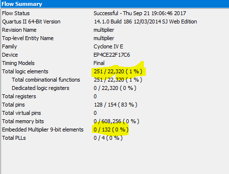
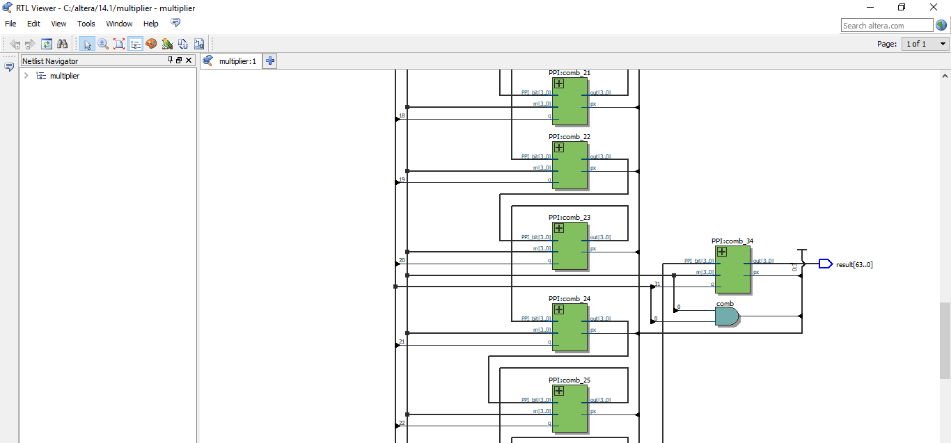
The output result shows that 251 logic element is used without using any embedded multipliers. It is a little larger than Altera megafunction. The RTL viewer is more complicated but acceptable.
RTL Viewer:
Sequential Multiplier
Assume the multiplicand (A) has N bits and the multiplier (B) has M bits. If we only want to invest in a single N-bit adder, we can build a sequential circuit that processes a single partial product at a time and then cycle the circuit M times.
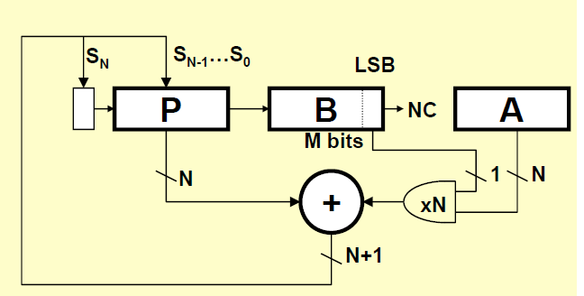
This is how the sequential multiplier is described. The description depicts it will be space efficient but the implementation doesn't show it is correct. Maybe, my design is not efficient, I am still learning the language.
The Code:
module multiplier (m, q, result);


parameter n=32;


//assign inputs and outputs
input [n-1:0] m, q;
output [n+n-1:0] result;
reg [n-1:0] A,B;
reg [n-1:0]P;
reg carry;


  assign result = {P,B};

integer i;


always
begin
#1
for(i=0;i<n+1;i=i+1)
begin
if(i==0)
begin
A=m;
B=q;
P=0;
carry=0;
end
else
begin
          {carry, P} = P + (B[0]==1 ? A : 0) ;
{carry, P, B} = {carry,P,B}>>1;
end

end


end


endmodule
The Result:
This supposed to be a small footprint and slower but the result shows that it has the biggest footprint. It locates 2,046 logic elements which are much more than the other methods.

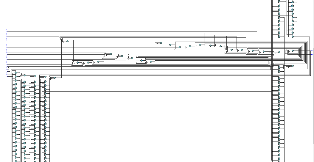
RTL Viewer:
The RTL viewer is much more complicated. It doesn't look like something understandable in a short time.
Test Code
When you design a circuit, you need to test it. But, the manual test can be time-consuming therefore it is good practice to write a test code for your design. You can test the design I have written up with the following test code. You can use Modelsim-Altera but if you don't want to install EDA tools you can use edaplayground.com. It has some limitations but easy to use. The following code doesn't test the all the input variables because of the limitations on edaplayground. You only need to change m and q variables in the for loops. The code below only checks for if the output is correct with the current inputs. There is no timing analysis.
module aritmetik_tst();

  // inputs and outputs for test circuit
  reg [31:0] m, q;
  wire [63:0] result;
  reg flag;
  integer i,j;

  // connection between testbench and design
  multiplier i1 (
    .m(m),
    .q(q),
    .result(result)
  );
initial
  begin
    m=0;
    q=0;
  end


always
begin                                                                     flag = 1;
  for (m = 1; m < 64; m = m + 1)
    begin
      for (q = 1; q < 64; q = q + 1)
       begin
        #1;
         if (result != m * q)
        begin
          flag = 0;
          $display("Test failed at %d x %d", q, m );
        end
       end //end of for(m)
    end//end of for(q)

  if(flag==0)
    $display("Test Failed, End of Simulation");
  else
    $display("Test Successful, End of Simulation");
$finish;
end

endmodule
Result:
FPGA is so flexible you can almost design everything but it may be time-consuming. It looks like it is better to use Altera functions and trust the vendor. Quartus is so sophisticated software and I think vendor optimise their functions with cooperation between EDA tool and underlying hardware.
Top Comments