


My last project:
Direct Fourier Conversion Software Defined Transceiver
turned out to be un-workable... I'm going to re-tool with a new board, and decided to start a new blog from scratch.
I ordered this board today:

It uses a KINTEX-7 FPGA chip XC7K325TFFG900. Notable differences from the Artix 7 chip/board are:
- Four transceiver QUADs for a total of 16 transceivers (vs. 1 QUAD on the Artix 7)
- PCIe x8 bus (vs. 2 lane PCIe bus on the Artix 7)
- 12.5GB/s transceiver speed (vs. 6.6GB/s on the Artix 7)
The availability of 4 QUADs should solve the fundamental problem I had with the previous experiment. It gives me 2 QUADs for PCIe x8, a third QUAD for the four optical transceiver channels, and the fourth for ?.
The sample transfer math (sample rate x 2 bytes per sample x 8 bits per byte x 4 ADCs)
- 4 2217s sampled at 61.440MHz (DC thru 10 meters) gives us: 61,440,000 × 2 × 8 × 4 = 3,932,160,000 bits per second
- 4 2208s sampled at 122.880MHz (DC thru 6 meters) gives us: 122,880,000 × 2 × 8 × 4 = 7,864,320,000 bits per second.
7,864,320,000 bps into 6.6GB/s doesn't fit! But it works with 12.5GB/s
The 2 lane PCIe gen2 bus will handle 2 * 4GB/s, ie 8GB/s transfer rate. Barely enough to keep up with one 4 x 2208 ADC board. The 8 lane board will transfer 8 * 4GB/s , ie. 32GB/s. This should be able to stay ahead of 4 2208 x4 ADC boards (31,457,280,000GB/s). This may or may not be ample. If not I move to an ultraScale chip which will support PCIe gen3!
I knew the transfer math wouldn't work with the Artix 7 chip when I started, but I wanted a (relatively) cheap "proof of concept" exercise. The Vivado Design Suite is free for the Artix 7 chips, but when you move up to a Kintex 7 they want $2995 for the privilege!!! Only by accident did I discover that Xilinx has a "voucher program" where some authorized Xilinx partners can offer a chip specific license with their boards. Alinx assured me I will be getting the voucher for the Kintex 7 XC7K325T chip by email. Lets keep our fingers crossed, otherwise its an expensive boat anchor.
============================================================
Problem of the moment:
Figure out why I'm loosing ADC sample in the fiber path.
============================================================
February 28, 2024
I received an email from Alinx the day after placing my order with a link to one large .zip file with all the documents/demos/etc. as well as the license for compiling the Kintex chip. The is MUCH better than my experiences purchasing the 3 previous boards from re-sellers. The bad news is that many of the files are only in Chinese, while the re-sellers had translated many of them. A friend suggested I try Google Translate. Turns out you can drag-n-drop a .PDF file with mixed Chinese/English and get back a nicely translated, readable document.
Have DHL tracking number, its current status is:
Shipment is on hold
CINCINNATI HUB - Ohio - USA
This just means its going thru customs. Scheduled arrival is March 7.
I compiled the LED test and KEY (ie. switch) test. for bring-up. I've built a simple PCIe/xdma design for basic testing. Converted a half dozen .PDF documents that pertain to the functionality I need.
============================================================
February 29, 2024
Shipment has departed from a DHL facility CINCINNATI HUB - USA
Which means its somewhere between Cincinnati and Denver. The sad part is that it will be in Denver within 24 hours, then USPS gets it and they take another week to get it to my door!
============================================================
March 1, 2024
Well, they surprised me, it arrived today. There's some issue with always booting reliably, but I (mostly) have it running alongside the old board:
$ getid; getid2
psv3 Fri Mar  1 21:21:23 2024
aurv1 Thu Feb  8 08:54:40 2024
$ sudo ./xdma_test
device: /dev/xdma0_
Detected XDMA AXI-ST design.
Found h2c_0 and c2h_0:
    Initiating H2C_0 transfer of 4096 bytes...
    Initiating C2H_0 transfer of 4096 bytes...
    Transfers completed. Comparing data... OK!
Found h2c_1 and c2h_1:
    Initiating H2C_1 transfer of 4096 bytes...
    Initiating C2H_1 transfer of 4096 bytes...
    Transfers completed. Comparing data... OK!
Could not find h2c_2 and/or c2h_2
Could not find h2c_3 and/or c2h_3
device: /dev/xdma1_
Detected XDMA AXI-ST design.
Found h2c_0 and c2h_0:
    Initiating H2C_0 transfer of 4096 bytes...
    Initiating C2H_0 transfer of 4096 bytes...
    Transfers completed. Comparing data... OK!
Found h2c_1 and c2h_1:
    Initiating H2C_1 transfer of 4096 bytes...
    Initiating C2H_1 transfer of 4096 bytes...
    Transfers completed. Comparing data... OK!
Could not find h2c_2 and/or c2h_2
Could not find h2c_3 and/or c2h_3
Success!

============================================================
March 2, 2024
I've made more progress in past 2 days then entire last attempt - helps to have the right hardware!
=============================================================================
After removing device:

Error opening device, error code: 2

=============================================================================
After rescan:

xdma0
psv5 Sat Mar  2 11:43:44 2024

=============================================================================
Running test:

device: /dev/xdma0_
Detected XDMA AXI-ST design.
Found h2c_0 and c2h_0:
    Initiating H2C_0 transfer of 4096 bytes...
    Initiating C2H_0 transfer of 4096 bytes...
    Transfers completed. Comparing data... OK!
Found h2c_1 and c2h_1:
    Initiating H2C_1 transfer of 4096 bytes...
    Initiating C2H_1 transfer of 4096 bytes...
    Transfers completed. Comparing data... OK!
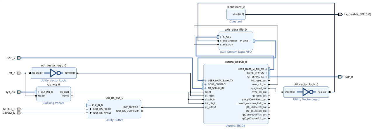
I'm writing to H2C_0 (host to card channel 0) which goes thru a 16 byte to 2 byte width converter and then into a fifo. The fifo is drained by the aurora Tx port. I have a 0B010 constant on the aurora loopback control port, which causes the data to immediately go the the aurora RX port. From there it goes into a fifo, then a 2 byte to 16 byte converter, which is drained by the C2H_0 channel of the xdma/PCIe bridge. In the above code snippet you can see the data travel thru and compare correctly on return.

Its taking path 2 thru this diagram:

The next step will be to add external ports to/from the SFP+ cages, which will allow me to send data out the fiber.
============================================================
March 3, 2024
I believe I have the first fiber working:
This is with an external loop-back connector plugged in:
device: /dev/xdma0_
Detected XDMA AXI-ST design.
Found h2c_0 and c2h_0:
    Initiating H2C_0 transfer of 4096 bytes...
    Initiating C2H_0 transfer of 4096 bytes...
    Transfers completed. Comparing data... OK!
And this is with it removed:
device: /dev/xdma0_
Detected XDMA AXI-ST design.
Found h2c_0 and c2h_0:
    Initiating H2C_0 transfer of 4096 bytes...
    Initiating C2H_0 transfer of 4096 bytes...
    Transfers completed. Comparing data...
Failure! Transferred data do not match!
Once I provoke the error replacing the dongle doesn't clear the error on next test. Not sure if I need to flush the channel or I need to reset the transceiver or ???
============================================================
March 4, 2024
I have all 4 transceivers running via 4 aurora 8B10B!!!

Note that only 2 can work at a time as there are only 2 h2c/c2h channels available on 7 series FPGAs. I will either have to somehow mux 2 transceivers to each channel, or step up to an ultra series FPGA, which support 4 h2c/c2h channels. I *think* I know which board I want to use, but need to find the buck$ somewhere...


============================================================
March 7, 2024
I designed a simple echo program for the AX7202 FPGA board (to be used for the ADCs):
All it does is echo everything it receives back out the xmit port. Not sure why, but I had to place that FIFO in between USER_DATA_S_AXI_TX and USER_DATA_M_AXI_RX. Without it bytes were often lost...
$ date
Thu Mar  7 01:29:27 PM MST 2024
$ while [ 1 ]; do sudo ./etest; sleep 1; done
Wrote 4096 bytes
Read 4096 bytes
Transfers completed. Comparing data... OK!
Wrote 4096 bytes
Read 4096 bytes
Transfers completed. Comparing data... OK!
Wrote 4096 bytes
Read 4096 bytes
 ...
This is connected to the master FPGA board's SFP port #1 with a 30 meter fiber cable. The test program starts 2 threads, the first does a 4096 byte DMA read, the second does a 4096 byte DMA write. After the 2 threads finish and join the read buffer is compared to the write buffer. Rinse, repeat.
I'm gonna let it cook for a few hours.
---
$ date
Thu Mar  7 01:29:27 PM MST 2024
$ while [ 1 ]; do sudo ./etest; sleep 1; done
Wrote 4096 bytes
Read 4096 bytes
Transfers completed. Comparing data... OK!

 ...

 Wrote 4096 bytes
Read 4096 bytes
Transfers completed. Comparing data... OK!
  C-c C-c
$ date
Thu Mar  7 04:17:14 PM MST 2024

$ grep OK etest.out | wc -l
9879

$ grep Failure etest.out | wc -l
0
So approximately 2 hours, 44 minutes, 39 seconds, 9879 successful passes without ERROR.
============================================================
March 10, 2024
I've finished a prototype of the ADC board:

I'm using a "pseudoADC' that clocks 2 byte samples out at a clock rate of 61.44MHz. These will replaced by actual LTC2217 ADCs later. Preliminary testing shows it will be on the hairy edge with 3 ADCs. No idea where the bottleneck is...
============================================================
March 18, 2024
I expanded my design to look like a 2 transceiver PCIe control card, and 2 independent 4 ADC cards:

The 1st set of 4 ADCs is connected to the 3rd aurora, and the 2nd set to the 4th aurora. They are free-running, just as the real ADCs will be. I connect them to the 1st and 2nd aurora with fiber cables, which are connected to c2h_0 and c2h_1. Then my software can read these channels for samples. Note that in the above design I actually have the plumbing set up a little differently for testing. It all seems to be working except that I appear to be loosing some samples when sent thru the 2 auroras. I'm going to write some test code next to help determine why.

