


Table of Contents
Introduction
Some Gowin FPGA parts contain not only the FPGA itself, but inside the package the manufacturer has fitted a PSRAM chip too! That’s really convenient if you need more RAM space than block RAM may ordinarily provide, but don’t want the overhead of designing in another chip onto the circuit board.
PSRAM is easier to use than SDRAM, but that can be simplified further by making use of Gowin’s ready-made “API” or library, better known in FPGA-world as IP.
This blog post walks through an example project that makes use of the PSRAM, not for any real purpose, but it exercises it by first writing data and filling up the entire PSRAM, and then checking the PSRAM contains what is expected, and then finally playing out each bit sequentially, using a couple of outputs on the FPGA, all ready to be observed with an oscilloscope.
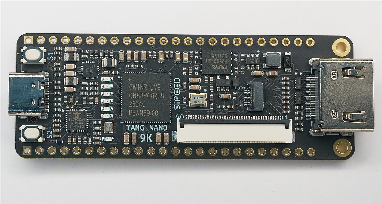
I used a Tang Nano 9k board, which contains the Gowin LittleBee series GW1NR part (the full part code is GW1NR-LV9QN88PC6/I5).
If you're new to Tang Nano boards, this blog post provides an introduction:
(+) Tang Nano Series and Gowin FPGAs for Beginners: A Practical Guide, Part 1 - element14 Community
Disclaimer: I used AI significantly to help me with the HDL code. This article however was written by myself, and I checked the VHDL code pretty much line-by-line to ensure it does what I expected it to do.
PSRAM Overview
PSRAM is cheaper than SRAM, because it doesn’t dedicate as many transistors per memory cell, and easier to use than SDRAM, because the refresh circuitry is on-chip. The PSRAM inside the GW1NR part has 64 Mbits of space, and those bits can be organized in a number of ways; In the screenshot further below it can be seen that I configured two channels of 32 Mbits each. The data bus is 32-bit wide (let’s call it a 32-bit “word”) and I chose to read/write in blocks of 8 words (this can be considered a “burst” of 32 bytes, but it’s easier for the rest of the blog post to express it as 8 words).
Since 8 words will be read or written, this means 8 clock pulses will be used to transfer the data in or out (plus however many pulses are needed beforehand to send the read or write command, and delay until the data is available).
The PSRAM requires a clock to operate, and it needs to be between 50 and 160 MHz. I went with 81 MHz, which isn’t completely arbitrary, because 81 MHz happens to be three times 27 MHz, which is the frequency of the crystal on the Tang Nano 9k board. An integer multiple like 3 is an easy thing for a phase-locked-loop (PLL) to achieve. Using the PLL entails using PLL IP incidentally, so now that’s two sets of IP that need to be included in the project, not a problem of course, that’s what the manufacturer’s IP library is there for.
Adding Gowin IP
After you’ve clicked on File->New and created a new project, you might create a first VHDL file called (say) top.vhd (this is assuming the VHDL language is being used for this project).
Next, click on Tools->IP Core Generator, and then navigate to the PSRAM Memory Interface HS selection as shown here and double-click to launch it.

Incidentally, if you want to ever review the configuration at a later date, go to Tools->IP Core Generator again, but this time look for a little folder icon above the IP list (the icon is shown boxed in orange in the screenshot above) and then navigate to a file with suffix .ipc which will contain your IP settings.
The screenshot shows the adjustments I made, and then I clicked on the Options tab.

Within the Options tab, I set the Burst Mode to 32 bytes (i.e. 8 words).

When you click OK, a few things happen. Firstly, the IP is generated and your project folder will now contain a src/psram_memory_interface_hs folder (or similar), and secondly the generator will dump some temporary content into the code pane. That temporary code contains a component definition and instantiation, both of which need to be copy-pasted into your main VHDL code somewhere. You can see where it needs to go by looking at my example top.vhd source file in the Github repo.
Adding the PLL IP is just as easy:

As before, a temporary file will appear and the VHDL there can be copy-pasted into your code.
VHDL Walk-Through
The VHDL code (the word code is being used colloquially, the term HDL source is often used) is far easier to understand by looking at a block diagram, split up to follow it better. The project implements within the FPGA three main phases of operations:
(1) Fill the entire PSRAM memory with a test pattern (the second channel uses an inverted version of the test pattern)
(2) Read the entire PSRAM contents, comparing each word with the test pattern
(3) Repeatedly read the entire PSRAM contents, outputting each bit serially onto a pin to observe with an oscilloscope; this is done for both channels, so a 2-channel ‘scope should show one signal inverted compared to the other.
The full block diagram is viewable here (open it in a separate window, and then you can pinch-to-zoom or whatever, while following the explanation in the rest of this blog post), and click here to see the top.vhd code.
Entity: Ports to the Outside World
The salmon-colored part, the entity called TOP, defines the external-facing ports for the hardware, in other words, the names of the signals that will make their way out to physical wires on the FPGA. You can see on the right side that led[1..0] refers to an array of two signals, so those obviously will be attached to two LEDs (these happen to be already soldered on the Tang Nano 9k board). The out_ch1 and out_ch2 will go to pins that can attach to an oscilloscope to see the bit pattern that is played out from the PSRAM.
All the ports labelled O_psram or IO_psram are actually not connected to physical pins on the Gowin part, but rather are connections from the FPGA chip inside, wired to the PSRAM chip next to it inside the package.
PLL Component
The two blue-colored items are known as components in VHDL, and one is the PLL, and the other is the PSRAM component. The PLL one is very simple externally, all it needs is a clock input (shown on the left side; I’m using the convention that all left side signals are inputs, and the right side signals are outputs). The PLL will multiply that clock input by three (provided it is configured for that in the IP configuration window, which I’ll get to). There is a PLL lock output, which is pretty important because it’s not a good idea to attempt memory writes with unstable clocking.
PSRAM Component
The PSRAM component looks complex, but (a) no code needed to be typed to create that component instance, since that was auto-generated as part of using that IP, and (b) if you look closely, a lot of the signals are doubled-up simply because the memory is being used in two channels.

All the signals are simple enough to follow. You can see from the diagram that the 81 MHz clock output from the PLL is wired to the memory_clk input to the PSRAM component. Many of the other signals are self-explanatory, for instance, you can see from the thick pink/magenta lines that there are two 21-bit address buses called addr0[20..0] and addr1[20..0], for the two channels. The VHDL code happens to connect them together, i.e. I intend to treat these two channels in a similar way (an example would be for left and right audio data) so I can access memory locations across the two channels in parallel.
The 32-bit data buses are shown with thick orange and light-blue connections attached. The orange ones are inputs to the PSRAM component for writing data, and the light-blue ones are outputs.
The init_calib0/1 signals go high when the PSRAM has initialized, and so the VHDL code will need to wait for that (and wait for the PLL lock) before performing read/write operations.
Also, the PSRAM component provides a clock output that is a divided-by-two version of its input clock, therefore it will be 40.5 MHz in my case. That clock is expected to be used as the clock for the rest of the user VHDL code (at least, that is what Gowin intends the user to do according to their documentation, so that’s what I did).
The remaining input signals cmd0, cmd1, cmd_en0, cmd_en1 are 1-bit signals that are used to control whether the memory is being read or written. The cmd0/1 signal needs to be high to perform writes, and low to read. The cmd_en0/1 signal needs to go high (i.e. asserted) for one clock cycle, to instruct the PSRAM component to accept the command.
I've now covered a fair portion of the project, and really very little VHDL needed to be written to achieve that, since those particular component declarations were created by the Gowin IP generator feature. It’s time to look at another part of the VHDL code.
Process: Asynchronous Reset
A VHDL process is a way of grouping up things that run sequentially. You can have many processes, they all operate concurrently with each other, but sequentially internally. The great thing about processes is that they allow the developer to implement registers that can store results, i.e. retain state, from one clock cycle, to be used in the next. This is super-important because without a clock, there could be glitches and you wouldn’t know precisely when results are valid, due to small delays in signals arriving at different inputs of logic gates. With clocked logic such delays do not matter, since there is time for logic outputs to settle, provided that happens faster than the controlled clock speed.
Registers are automatically inferred into a design, whenever the developer uses a pattern in their VHDL code that looks like this:
process(clk_out, reset_n)begin if reset_n = '0' then -- reset code sits here cmd0 <= ‘0’; elsif rising_edge(clk_out) then -- outputs will have registers cmd0 <= ‘1’;end process;
Processes have a ‘sensitivity list’, in this example that consists of the signals called clk_out and reset_n (the _n is a convention in signal naming to show the reader that the signal is active low, like many reset lines are). Whenever any of the signals in the list changes, then the rest of the content within the process will run.
Whenever the sensitivity list is followed by that line with the VHDL statement rising_edge, then the VHDL synthesis tool will understand that to mean registers are needed. Thus, the example above will implement a register that outputs the value ‘1’ to an output signal called cmd0 on every rising edge of the clock. On its own that is not very useful of course, but as will be seen in the rest of this PSRAM project, the process can do a lot more.
The reset_n signal is checked outside of that rising_edge statement, and therefore the reset operation is asynchronous to the clock.
The diagram below shows (only the gray box is of interest here) what signals are affected when the asynchronous reset occurs. All the signals listed there are initialized to known values during that asynchronous reset.

Here’s a snippet of the VHDL code for the asynchronous reset. The strange syntax wr_data0 <= (others => ‘0’); is a way of setting a signal array all to zero but there are other ways too; you could write databyte <= B”00000000”; for say 8-bit bus signals.

Function
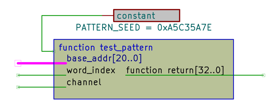
Before we look at the remainder clocked portion of the process, it is worth mentioning functions. They are bits of reusable HDL that can accept various inputs and return one signal or array. For this project, a function called test_pattern is used to provide a 32-bit value based purely on a seed, address (base address which doesn’t change for a burst of 32-bit data), the index into the burst, and the channel number.
When this test_pattern function is used, the base_addr signals will end up being the address supplied to the PSRAM component.
This function is not that important to the task at hand (i.e. writing and reading PSRAM content), the test_pattern function is merely used to supply something interesting to write into the PSRAM, and to check that it matches when reading.
In a real project, perhaps the data would arrive from an ADC or a PC, so this test_pattern function would not be needed (although, it may well be useful to perform a memory self-test on startup, for really critical applications).
Process: Registered Portion
The asynchronous reset part of the process has been discussed. The remainder of the process contains the majority of the project. Things happen in sequence, with a bit of work happening on each clock cycle, depending on the state of various signals that were registered on the preceeding clock cycle. The first part of the VHDL code in this portion checks to see if a read operation is occurring, which would have been initiated beforehand on an earlier clock cycle.
Read Operation Underway
The first two lines within the elseif statement are responsible for setting the cmd_en0/1 signals low, in case there were high in a previous clock pulse, because the read/write commands require the enable signal to go high just for one clock cycle.

Next, a signal called rd_data_valid0 is checked, and this is actually from the PSRAM component. The documentation for that shows the signal goes high when the rd_data[31..0] signals are outputting valid data (in response to a read command that would have been requested in an earlier clock cycle).

From the VHDL snippet above, it can be seen that if the data valid signal is high, then the values on the read data bus rd_data0[31..0] get stored using registers into an internal signal array called last_rd_data0[31..0], and also gets compared with a test pattern. If the test pattern does not match, then error_ch0 gets registered high (this is used to light up an LED).
The if state = PLAY_CAPTURE line concerns a signal array that is used to implement a state machine, which will be discussed shortly, but for now, the interesting bit is seeing what happens to the read data; it gets stored in the correct position within an array of signals called play_buffer0, which happens to be a very long array of 256 bits, which is the length of 8 words. The VHDL synthesis tool will create a 256-bit register for that. You can guess from the signal name, that it will be used to play out the individual bits serially, just for the demo, no real purpose. There is identical VHDL code (not shown) for the second channel (channel 1).
The diagram below shows a high-level graphical representation of all of the signals involved in that VHDL fragment. The thick light-blue lines are the read data lines from the PSRAM component. The signals in the boxes on the right indicate what gets checked or what gets stored. The test_pattern function is actually used twice, once for each channel. On the right side, you can see that error_ch0/1 signals are generated, they were visible in the earlier block diagram that showed the salmon-colored entity, and they go to ports that attach to LEDs on the Tang Nano 9k board.

Calibration and PSRAM Write
If you recall, it’s necessary to wait on power-up for the PSRAM to be ready for read/write operations, and the PSRAM component reports it is ready by asserting the init_calib0/1 signals (see the first block diagram which showed the PSRAM component). In the diagram that showed the async reset (gray colored box) it could be seen that a signal called state was given an initial value of WAIT_CALIB. The next part of VHDL code within the process block checks the state value. The diagram below looks complicated, but really it can be divided into three, representing three case statements, each one checking the state value.
The top statement checks if the state is WAIT_CALIB, and if it is, then it simply initialises various signals listed in the box, including setting the address lines to zero (the two PSRAM channel address buses are continuously driven from the current_addr register output), and then will only set the state to WRITE_CMD if the PLL is locked and if the init_calib0/1 signals are high, otherwise, it remains in WAIT_CALIB on each clock pulse.
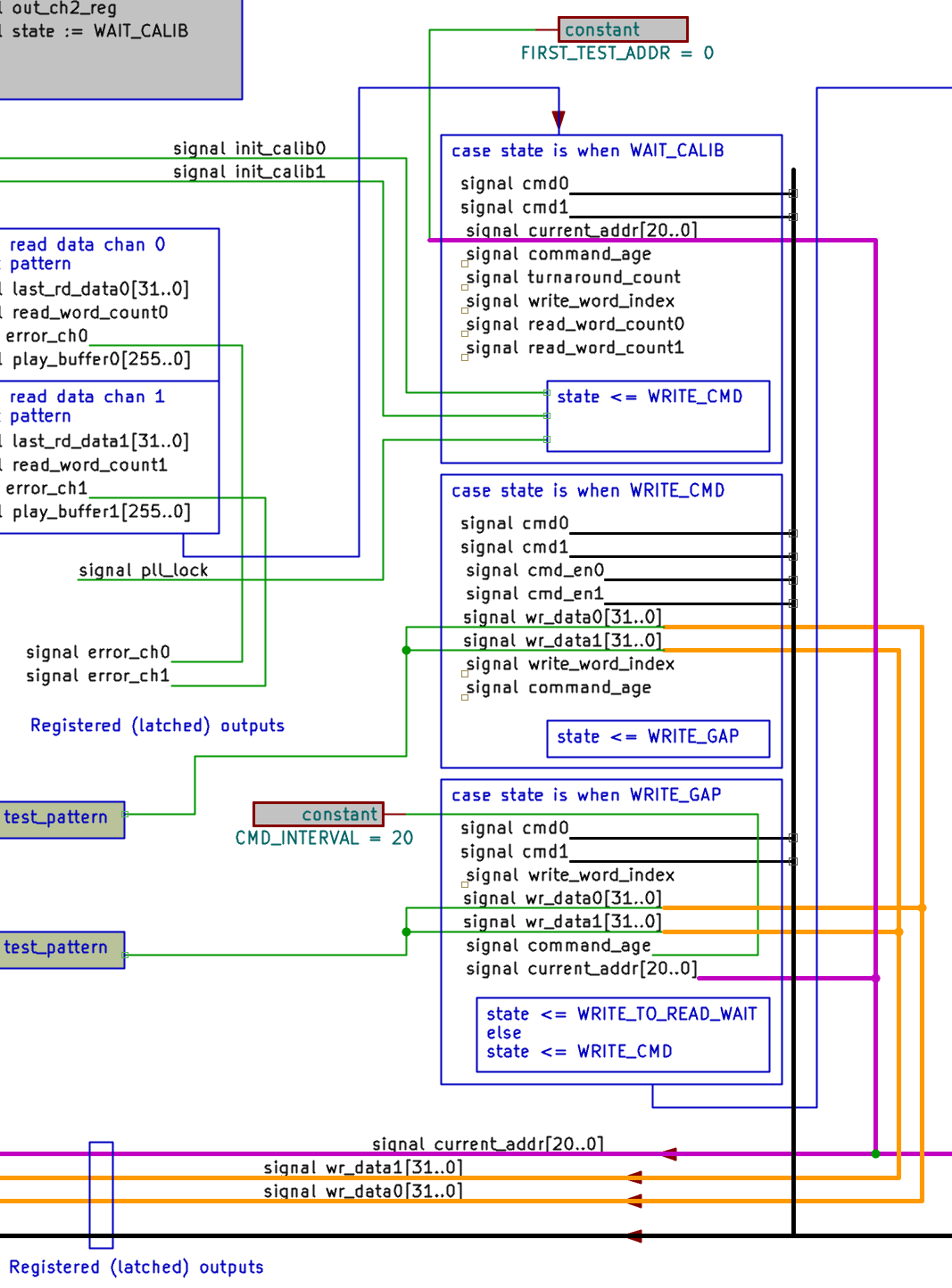
The next state in the diagram above is WRITE_CMD, and when that occurs (well, on the next clock pulse after it was set in the previous case statement), a test pattern is applied to the wr_data0/1 signals, and the cmd0/1 and cmd_en0/1 signals are all set high to initiate the write sequence and write the first word.
The waveform diagram (aka timing diagram) from the Gowin documentation shows the write sequence. The WRITE_CMD state is responsible for just that first relevant clock pulse (numbered pulse 2 in this diagram) and then the state is changed to WRITE_GAP for the next clock pulses which will arrive, which is discussed next.

In the WRITE_GAP state, the code snippet here shows that the write data bus to the PSRAM component is set to a test pattern, and the word index is incremented, so that a unique test pattern is supplied on subsequent pulses. Thus, the state remains set to WRITE_GAP until all the data in the burst (indicated as Data1 to Data7 in the waveform diagram above) has been supplied to the PSRAM component.
However, notice in the code snippet that the WRITE_GAP state isn’t exited immediately after the burst is complete. A signal array called command_age happened to be initialized to zero in state WRITE_CMD, and it is incremented by 1 on each clock pulse in the WAIT_GAP state. Once that reaches a constant value (CMD_INTERVAL-1) then the state is allowed to change, either back to WRITE_CMD for the next write burst, or to WRITE_TO_READ_WAIT if the PSRAM is fully written. The reason for that delay is that the PSRAM cannot accept write bursts immediately one after the next; it needs a short pause.

That completes the PSRAM write operation discussion; when the state finally changes to WRITE_TO_READ_WAIT as shown in the above code snippet and block diagram, data can be read.
One minor point: the constant ADDR_STEP is 16, although I initially thought it ought to be 8, since we are stepping through 8 words at a time. It appears to be due to the PSRAM part used by Gowin, and the way they chose to implement their IP. I didn’t find any documentation on this particular point (and some examples of PSRAM usage only write/read one burst, so it’s not possible to figure out!).
PSRAM Read during the Verification Phase
Again the block diagram looks like a lot, but it can easily be covered piece-by-piece. But first, you may be wondering how come there are no thick light-blue colored lines from the PSRAM component, which represented the 32-bit read data bus. That’s because those signals were covered in the Read Operation Underway section earlier, where each word was compared with the test_pattern function result, and, if in PLAY_CAPTURE state, the burst was filled into a 256-bit register called play_buffer0 (and play_buffer1 for the second channel). The three states in this block diagram are concerned with setting up the read operation.
Firstly, the WRITE_TO_READ_WAIT state is used to introduce a short gap after all those write operations earlier. The VHDL code is similar to the inter-write burst gap code seen earlier (but just with a different counter with the signal name turnaround_count rather than command_age), so it won’t be discussed further. The state moves to READ_CMD after the delay.
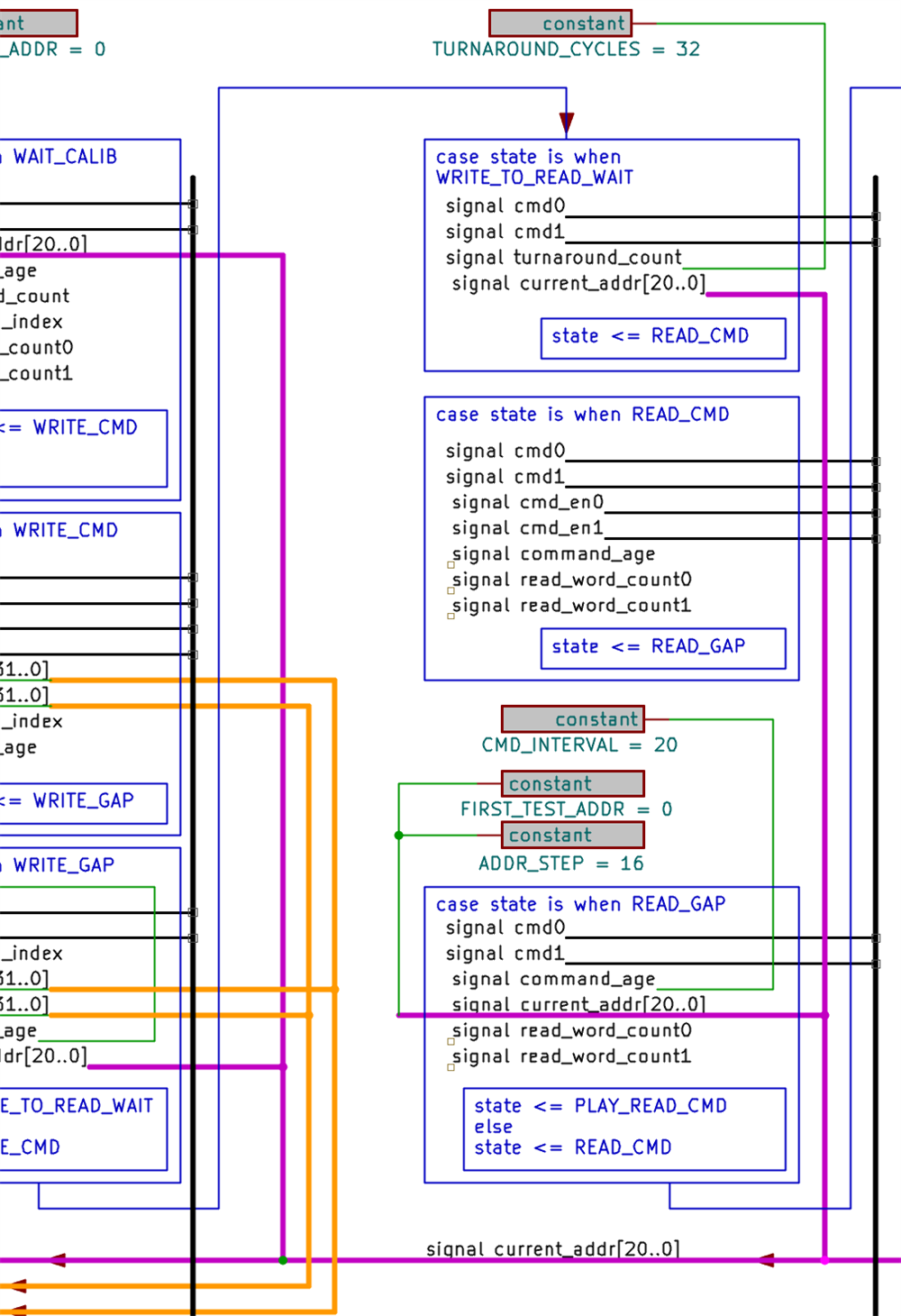
In the READ_CMD state, cmd0/1 are set low to indicate a read operation request, and cmd_en0/1 are set high so that on the next falling clock pulse, the read operation is started, and the state moves to READ_GAP.
The PSRAM component will need a few clock cycles to present the output on the data buses for each channel, and will indicate with an rd_valid signal going high. All that has already been covered in the Read Operation Underway section, so all that needs to occur in READ_GAP is to just remain in that state long enough for the entire burst to complete, and remain in the state a bit longer, as the PSRAM component requires. Again, command_age is used as a counter for this, and after the count is complete (i.e. it reaches CMD_INTERVAL-1), the state moves either back to READ_CMD for the next read burst to be initiated, or the state moves to PLAY_READ_CMD if the entire PSRAM memory has been fully read.
By the time the state reaches PLAY_READ_CMD, all the PSRAM contents will have been read once, and compared to the test pattern, and an error LED, one per channel, will be lit if the pattern isn’t what was expected.
PSRAM Read: Playback
This project has already demonstrated PSRAM read since the memory contents were read to compare against the test pattern, but just for completeness here is the diagram containing the remaining states that show how the playback phase of the project works.
The PLAY_READ_CMD state simply initiates a PSRAM read operation (by setting cmd0/1 low, and setting cmd_en0/1 high), identically to what occurred in the earlier READ_CMD state. The only small difference is there is no command_age to initialize, because the playback is deliberately at a lower frequency (to make it easy to see with a low-cost ‘scope) and so there will be plenty of time between each read burst.
The state moves to PLAY_CAPTURE where, as discussed before, each word within the bursts is filled into the 256-bit play_buffer0 and play_buffer1 registers. The state moves to PLAY_SERIAL once the burst is complete, i.e. the 256 bits are filled.
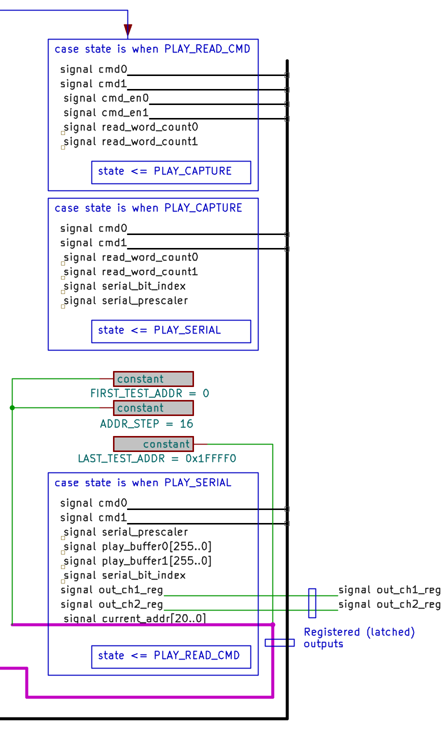
The PLAY_SERIAL portion is displayed below. What happens is that an internal signal array called serial_prescaler counts up on each clock pulse, until it reaches 31 (i.e. total of 32 clock pulses from zero), since a lower output rate is desired. At that point, one bit from play_buffer0[255..0] is registered out to a signal which is attached to a port in the top entity, so it can be observed on a physical pin on the Tang Nano 9k board. A similar thing is done with the other channel. Once all 256 bits have been output in this fashion, the address bus value is incremented to point to the next desired burst of data, and the state moves back to PLAY_READ_COMMAND which will initiate the next read sequence.

Building It
The Gowin FPGA Designer application has tabbed panes on the left side. Select the Process tab to see a list of tasks that can be launched. Double-click on Synthesize, and if all goes well, that icon will change into a green circled check-mark.
At this stage, pins need to be assigned, and clocks need to be identified (so that the FPGA can fit the synthesized design in a sensible way inside the FPGA, to maintain good performance on the specific signals that require it).
Both of these things are expressed in constraint files that can be created using the graphic interface if desired.
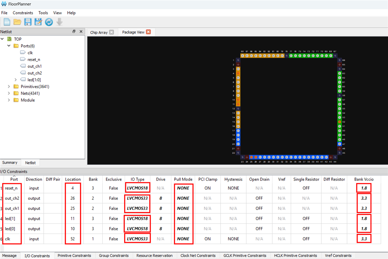
In the same Process tab pane, click on FloorPlanner and then in the window that will appear, there will be a graphic area. Above that, click on Package View. You can then drag-and-drop port signals from a pane on the left, onto the desired chip pins. This project has 6 ports to assign. The diagram here shows the six connections that were chosen. The reset_n line was attached to the button S1, and clk goes to the connection to the 27 MHz oscillator.

The screenshot here shows how the FloorPlanner screen should finally look like. Pay special attention to the settings, because the Tang Nano 9k has a mix of 3.3V and 1.8V connections. The 27 MHz oscillator for instance outputs a clock at 3.3V logic levels, whereas the LEDs and buttons are attached to 1.8V.
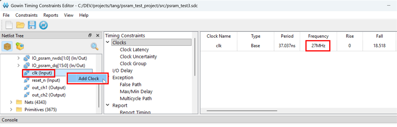
For the clock constraint, double-click on the Timing Constraints Editor in the Process pane, and then find the clk signal in the Ports list, and right-click to add the clock constraint. I typed 27 for the frequency, and then clicked OK.
Does it Work?
Yes : ) After building it (i.e. in the Process pane, double-click on the Synthesis tab, and then double-click on Place&Route, and hope they both change to green-circled check-marks) the Gowin Programmer was used to transfer it into the Tang Nano 9k.
If you’ve not used the Programmer before, be aware that the Tang Nano boards seem to require a USB-A-to-C cable (despite USB-C-to-C appearing to initially work), the supplied cable may be faulty (mine was), and when launched, the Programmer chooses one of two communication channels; I had to swap to the second channel for successful programming).
Anyway, once it was programmed, all LEDs were off, which at least meant there was a chance the code was successfully running!
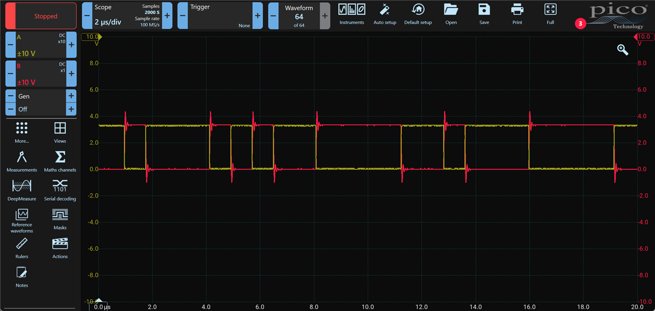
I attached the oscilloscope probes (not very well) and you can see the two outputs are complementary and at the expected data rate. I didn’t try to capture with a logic analyzer and decode it back to the original data.
Summary
Some of the Gowin parts feature built-in PSRAM. The Tang Nano uses a GW1NR device with 64 Mbits of PSRAM, and it is quite easy to use by adding Gowin IP to the project. PLL IP was also used, to multiply the crystal clock source to a usable frequency.
The PSRAM was configured to operate with 32-bit wide data buses, in two 32 Mbit channels.
The VHDL code implemented a state machine that waited for the PSRAM to be ready/calibrated, and then the entire two channels were filled with test pattern data, in bursts of 8 words. The state then transitioned to allow reading of the memory to confirm it was correctly filled, and then the memory could be repeatedly read out at a slower rate for serializing the data out of a couple of FPGA pins.
Obviously, this project on its own doesn’t serve a useful purpose, but hopefully with the VHDL description and diagrams, it is now easier to use the PSRAM in other projects.
Thanks for reading!
-

dang74
-
Cancel
-
Vote Up
0
Vote Down
-
-
Sign in to reply
-
More
-
Cancel
Comment-

dang74
-
Cancel
-
Vote Up
0
Vote Down
-
-
Sign in to reply
-
More
-
Cancel
Children