


Table of Contents
Introduction
The Tang Nano series uses FPGA parts from Gowin, and they are available in a range of sizes. The photo here shows the 9k and the 20k variants (the 20k one happens to be on a physically smaller board, but is more powerful). There is also a 1k variant, but it was missing from the photo shoot. I misplaced it when I took the photo : (
These boards mostly come with a USB connection at one end, some have a HDMI connector at the other, and all remaining signals (it’s an FPGA board, so you can assign what you want to them all) are on solderable pin header connections, but there’s also a flat flex connector intended for a TFT screen, but again, as it’s an FPGA board, you could repurpose these connections for something else if desired.
In terms of other built-in hardware, there’s a micro SD card slot on the underside, and a few buttons and an array of LEDs on the two boards in the photo.
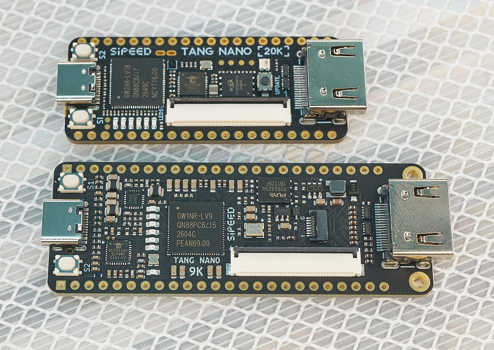
This blog post discusses how to go about using these boards. This first blog (it will be a two part series) explores what’s on the boards and FPGAs, and highlights a few differences across them.
Microcontroller vs FPGA: Pros and Cons
You can do a lot with a microcontroller, but sometimes very deterministic signals are needed. The Pi Pico often helps me here; it contains special hardware named PIO, which can be used to create interfaces with specific timing. It’s really excellent, but some things just push it more than what it was intended to do. I liked that the Tang Nano boards were quite low-priced (for FPGA boards) and already contain some built-in interface connectors for video and displays, and the development environment seemed fine to work with.
The downside of working with FPGAs is that you’re not really coding; you’re describing actual logic signals and things that you want turned into registers and gates. There’s a bigger learning curve (in my opinion) than working with plain software; you not only need to learn to work with the language (known as a hardware description language [HDL]), but also have an awareness about digital circuitry and recognizing what to type to infer the implementation you want. There’s also a learning curve in developing circuits that use clocks to push processing results piece-by-piece through the entire circuit being implemented. It also becomes important to recognize what is worth doing in HDL and what is worth doing in microcontroller code, so developing across two different domains and testing all that, is yet another overhead. On the plus side, the benefits can be huge of course; great performance is possible!
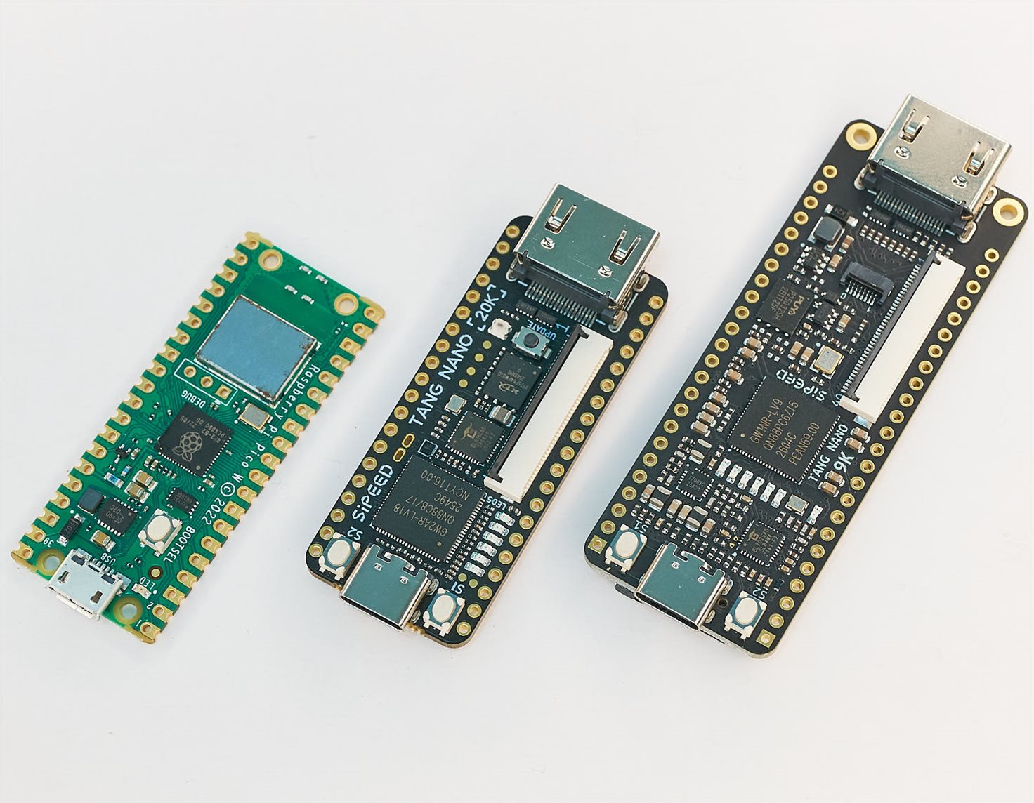
What’s Inside the FPGAs?
The Tang Nano boards contain an FPGA from Gowin Semi (either LittleBee series or Arora II depending on the Tang Nano board selected), plus a bit of extra hardware so that Flash memory can be configured with the ‘program’ (it’s not really a program, it is called a bitfile or bitstream) that is needed to bring up the FPGA. The bitfile literally configures individual logic bits inside the FPGA, so that it can do what you want.
Here’s an attempt at an explanation. The diagram here shows what’s inside Gowin FPGAs (some Gowin parts feature additional functionality). From a bird’s-eye view, it can be seen that the most common thing is a Configurable Function Unit (CFU) and there are lots of them (typically hundreds). Each CFU can perform a small amount of logic functionality, and there are interconnections possible across the entire chip, using a feature known as routing, indicated with red lines in the diagram. Part of the bitfile programs up the CFU to perform what it needs to do, and part of the bitfile represents what routing is needed between them all.
Routing can be a bit slow, so there are also a few configurable clock signals that fan out from the center (yellow lines), to allow each CFU to latch operation results on clock edges and synchronize the project. The FPGA contains oscillator and frequency multiplication capability (PLL), so that all you need to do is attach a crystal and you can derive several clock frequencies from that.
All around the chip are the input/output blocks, which can operate at different logic levels in banks. The I/O blocks take configuration from the bitfile, to determine if they should become inputs or outputs, what drive strength, and whether differential signals are required and so on. The I/O blocks connect to the routing, in order to ultimately make a connection to a CFU, not necessarily a CFU closest to an I/O block. Each I/O block can contain several GPIOs incidentally, or can be grouped for (say) differential input or output.
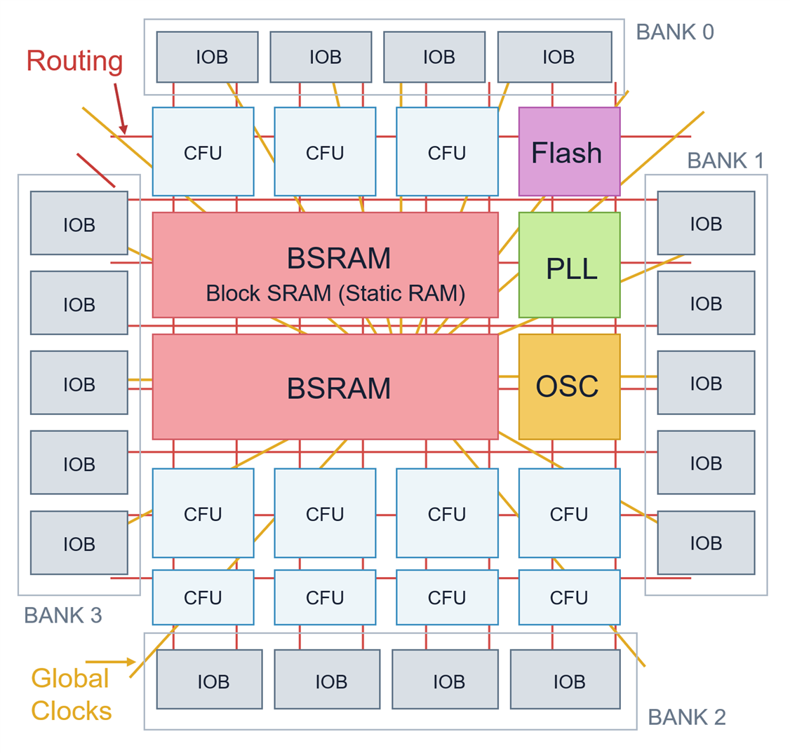
Zooming in a little bit into a CFU, and you’ll see this:
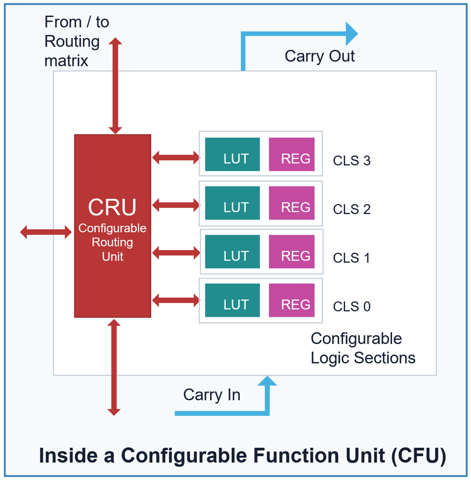
The routing unit is used to attach to all the routing, and, again based on bitfile content, will become configured when the FPGA starts up and loads, to pass signals between different CFUs or other entities, and also between the entities within the CFU.
Ordinary combinatorial logic (such as AND, OR gates) can be implemented with memory tables (for instance, for a two-input AND gate, you could call the inputs two address lines, and store the values 0, 0, 0, 1 in memory address locations binary 00, 01, 10, 11) and so it’s no surprise that the Look-Up Tables (LUTs) could be thought of as RAM that is loaded from the bitfile, to create all the logic that was expressed in the code (actually HDL, or Hardware Description Language) that the developer wrote to get turned into the bitfile.
The registers combine with the LUTs to produce clocked logic circuits, and these can (for instance) get inferred when the user types particular HDL content.
Particular operations need to happen speedier than routing, so carry logic (used for arithmetic) can span to the next consecutive CFU; that’s more efficient than trying to make the routing do it all, and the FPGA compiler is smart enough to know when to use the carry logic rather than routing.
Memory and Flash
Since the LUTs within the CFUs are implemented using RAM, they literally can be used as RAM too, known in Gowin terminology as Shadow SRAM (SSRAM), which is useful, because the CFUs are scattered across the chip, and hence the very local memory can be fast, but you can’t store a lot (16 x 4 bits per CFU). It also eats up into configurable logic of course. If you can tolerate slightly slower, but more abundant amounts of RAM, then one could make use of larger blocks, called Block SRAM, which take a bit more routing to access; BSRAM is not as local. The Gowin FPGAs used in the Tang Nano boards support access to the BSRAM using a single or dual port (i.e. a read and a write port) and can be used in a few defined bit widths, up to 32-bit wide, and you can access up to 16k addresses per BSRAM block (i.e. 2^14, since there are 14 address lines internally per BSRAM).
Many FPGAs require a separate Flash memory chip to contain the bitfile (or the bitfile may be transferred on power-up from a microcontroller) but some of the Gowin FPGAs used in the Tang Nano boards have built-in Flash for device configuration. Even better, some of that is accessible as “user flash”! It would be very feasible to implement a small computer processor inside the FPGA, and have the user flash contain the firmware, for instance.
A huge feature is that some of the Gowin parts contain memory chip internally too. For instance, the Tang Nano 9k board features a Gowin FPGA with 64 Mbit of PSRAM (an easier-to-use form of memory compared to SDRAM). The Nano 20k contains more conventional SDRAM.
FPGA Comparison
| Board | Nano 1k | Nano 9k | Nano 20k |
| FPGA | GW1NZ-LV1QN48C6/I5 | GW1NR-LV9QN88PC6/I5 | GW2AR-LV18-QN88C8/I7 |
| LUTs | 1152 | 8640 | 20736 |
| BSRAM | 72 kbit | 468 kbit | 828 kbit |
| Multipliers | n/a | 20 (18x18) | 48 (18x18) |
| On-chip User Flash | 64 kbit | 608 kbit | n/a |
| On-chip SDRAM | n/a | n/a | 64 Mbit |
| On-chip PSRAM | n/a | 64 Mbit | n/a |
For more detail on the FPGAs, check out the Gowin Documentation Database.
Tang Nano Board Differences
The actual FPGA chips on each board were compared in the table above. The Tang Nano boards have some differences between them, beyond the FPGA chips.
| Board | Nano 1k | Nano 9k | Nano 20k |
| On-board Flash | n/a | 32 Mbit | 64 Mbit |
| On-board RAM |
IPS6404L-SQ-SPN PSRAM footprint, unpopulated |
n/a | n/a |
| HDMI Output connector | No | Yes | Yes |
| SPI LCD connector | No | Yes | No |
| Micro SD socket | No | Yes | Yes |
| LEDs | Single (R, G, B) | 6 (row) | 6 (row) and 1 x NeoPixel (WS2812) |
| Audio | No | No | I2S DAC/Amp |
| Adjustable Freq Synth | No | No | Yes (MS5351M 25MHz xtal) |
| I/O Logic Levels | 3.3V | 3.3V, some 1.8V | 3.3V |
The I/O logic levels are something to watch out for on the Tang Nano 9k; not all are 3.3V.
Tang Nano Pinouts
The documentation for the Tang Nano boards is pretty good; there are schematics downloadable from Sipeed, and the actual FPGA datasheets and so on are available directly from the FPGA manufacturer website (GOWIN).
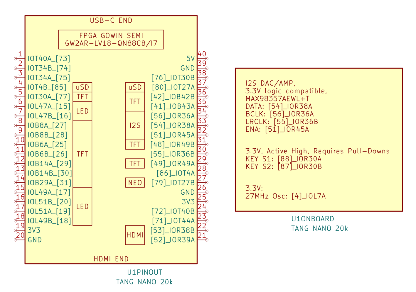
Still, there’s a lot spread out to make sense of. I decided to make some simpler-to-understand symbols, although one will still need to consult the schematics, especially for the on-board features.
The naming of the I/O pins looks a little confusing. The Gowin terminology is to label them beginning with IO, followed by a character T, B, L or R, which represents the top, bottom, left or right side of the die, and then a number which happens to represent either the column or the row number of the CFU (Configurable Function Unit) that I/O pin is close to, just for convenience. Finally, the last character indicates if other pins are close to the same CFU column or row, since useful relationships may be possible between otherwise same-named pins, for instance, IOT16A and IOT16B would identify IO pins at the top of the die, both close to CLB column 16, and can optionally operate as a differential pair.
For the symbols, I stuck with the Gowin terminology, but also added [nn] to the I/O pin names. The [nn] value is the physical pin number on the FPGA chip.
Another important point: on all the Tang Nano boards described here, the voltage labelled connections on the headers are all _outputs_. The only source of power should be from the USB-C connector.
Tang Nano 1k Pinout
Useful links: Tang Nano 1k Schematic, Tang Nano 1k Sipeed Wiki Page
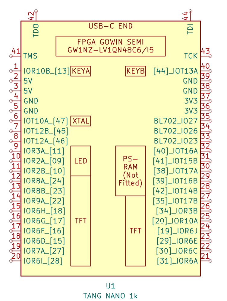
The Nano 1k exposes 32 IO connections onto the 40-way header, but notice that nearly all are already allocated a purpose, for instance, the Nano 1k has two push-buttons built in, and those are to IO pins labelled KEYA and KEYB in the symbol below. Lots of pins also go to the flat flex TFT connector on the board, and those pins are labelled TFT in the symbol. Of course, if you’re not actually connecting a TFT, then you could use those IO pins for any other purpose.
Note that the thee pins labelled beginning with BL702 are not attached to the FPGA, they can be ignored (they attach to a USB microcontroller on the Nano 1k board).
Also, be a little careful when counting pins on the Nano 1k, because there are 22 pins per side, not 20, because two pins per side expose connections for JTAG (unnecessary to use normally), I’ve labelled them pins 41-44 in the symbol below.
Tang Nano 9k Pinout
Useful links: Tang Nano 9k Schematic, Sipeed Tang Nano 9k Wiki Page
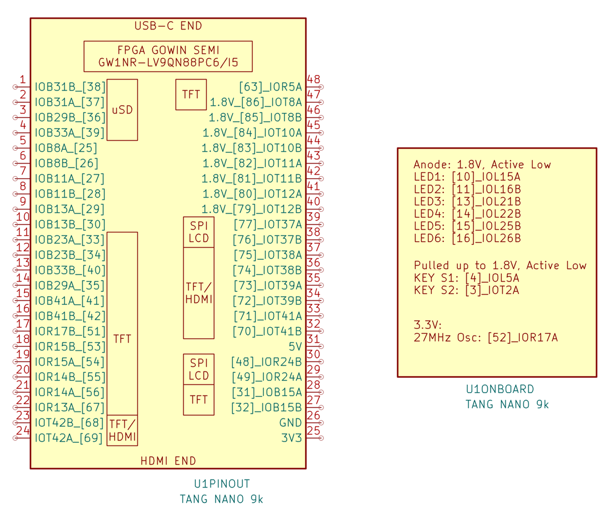
The Nano 9k is one of the physically larger boards in the family. It has 24 pins per row, and has built-in HDMI and micro SD slot, unlike the Nano 1k. Plus, the Gowin part used on the 9k contains 64 Mbit of PSRAM.
Notice that the on-board LEDs and buttons are wired to 1.8V. Some of the header pins are wired to 1.8V IO pins too.
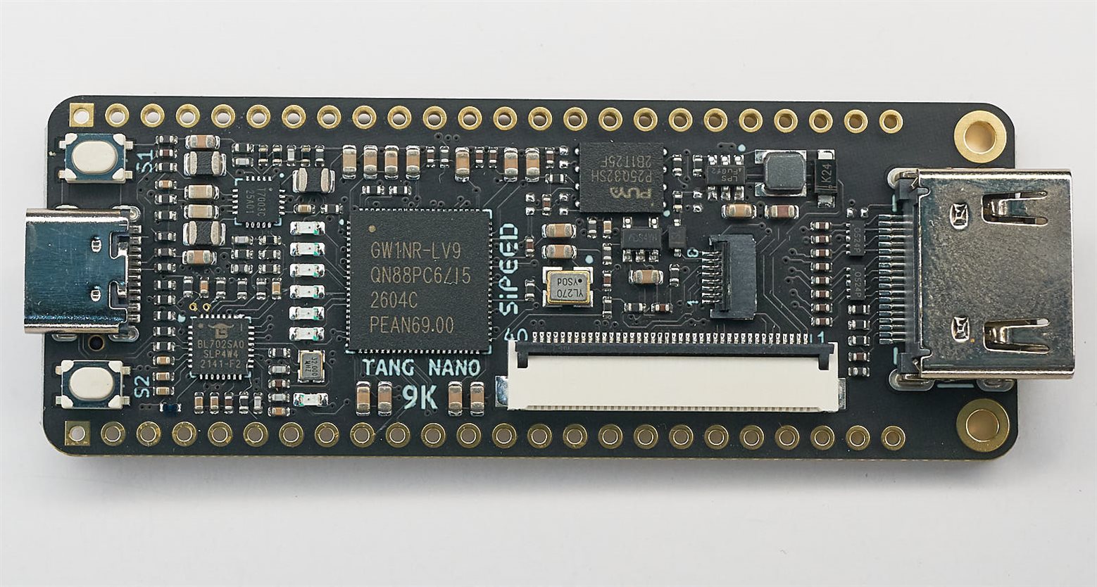
Here are some close-up photos of the board, the black PCB isn't too easy to photograph well, unfortunately. To the left of the HDMI connector, above the TFT flat flex connector, is a smaller flat flex connector for SPI LCD screens.
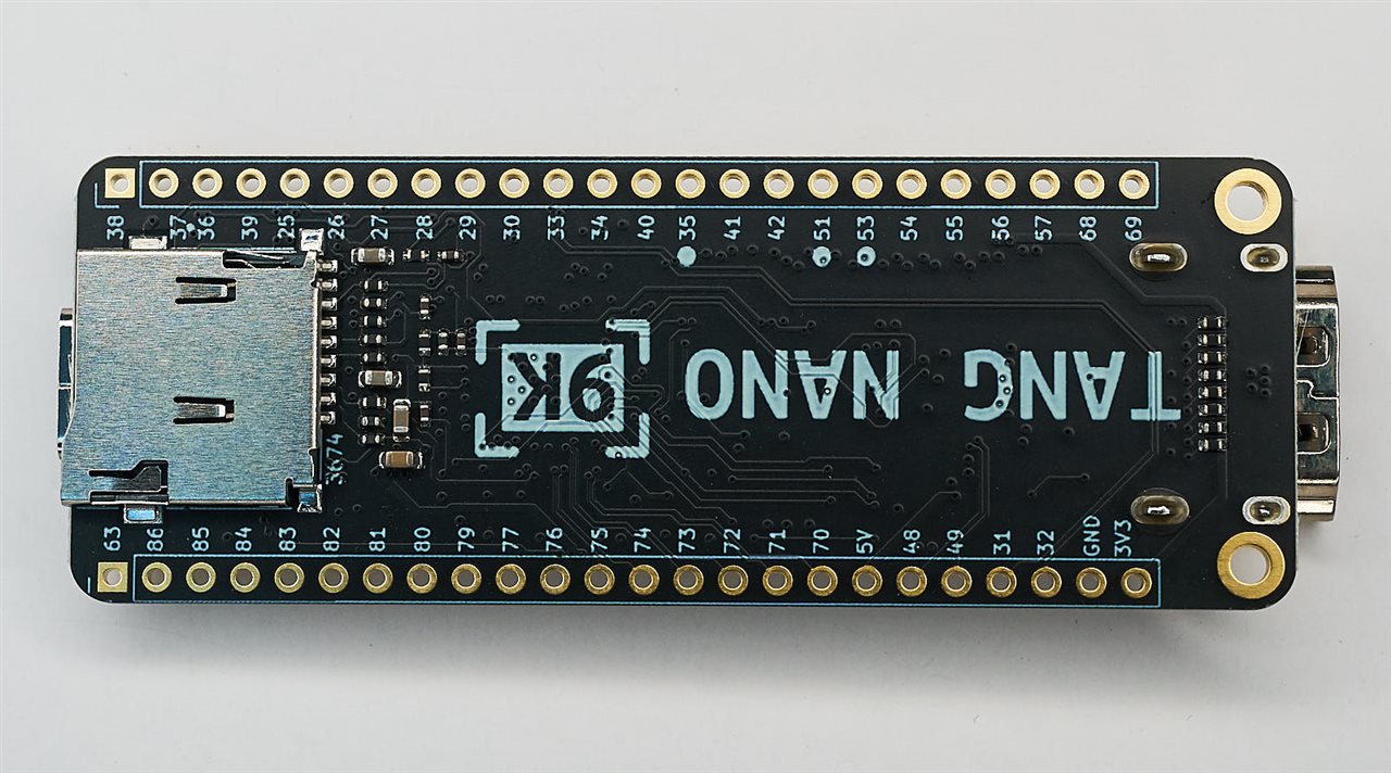
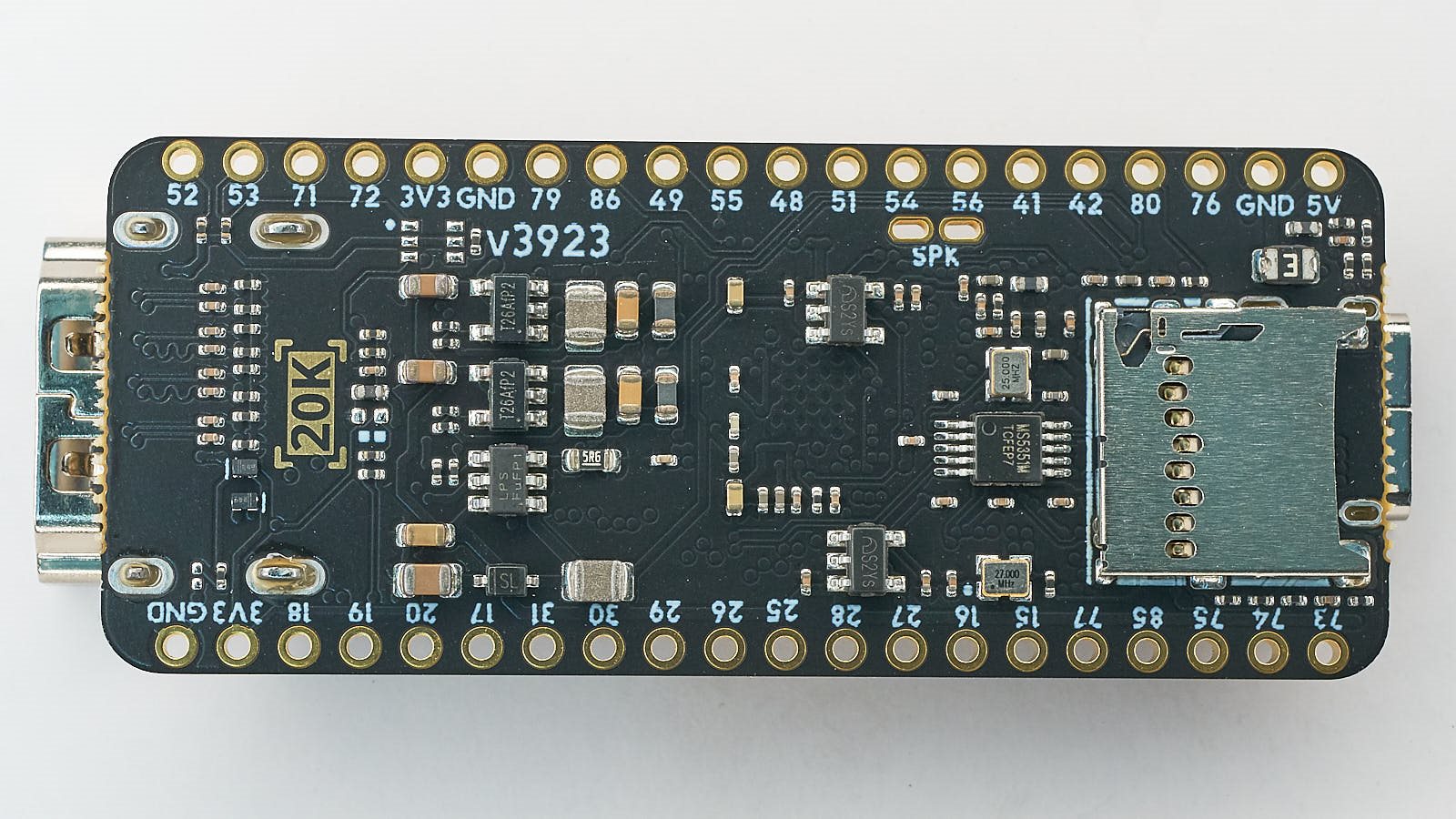
Not much on the underside, apart from the micro SD socket.
Tang Nano 20k Pinout
Useful links: Tang Nano 20k Schematic, Sipeed Tang Nano 20k Wiki Page
The Nano 20k is a 40-pin board. Like the other Nano boards discussed above, most of the IO pins are already assigned but you’re free to use them for other purposes if there’s no clash. Interestingly, the Nano 20k has some pins wired to an I2S DAC/audio amplifier (MAX98357). There are a couple of pads not shown on the symbol, that can be wired to a speaker.
Photos:
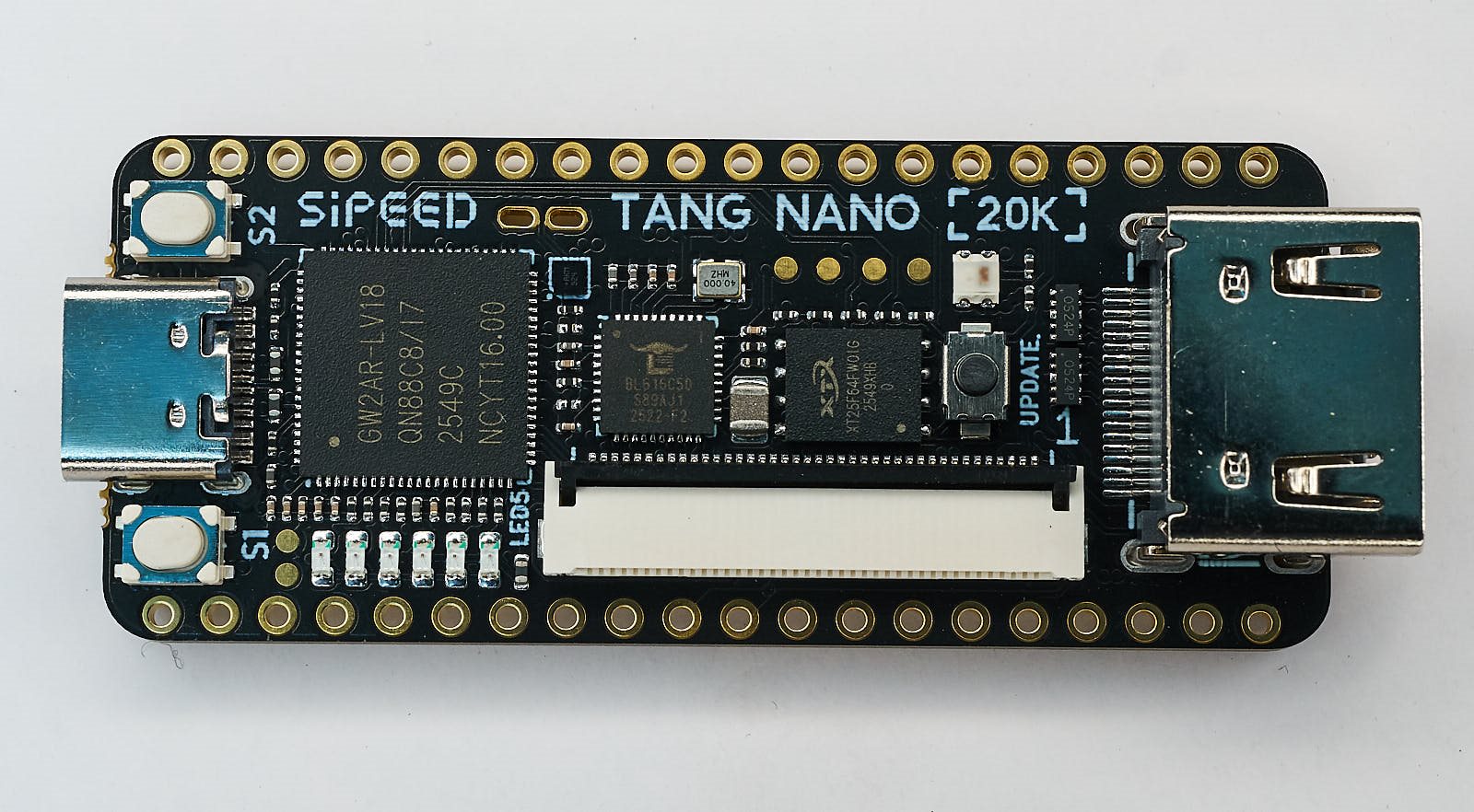
There's a nice frequency synthesizer IC on the underside, MS5351M, which is compatible with Si5351A.
Development Environment and Programmer
I installed GOWIN FPGA DESIGNER v.1.9.11.03 Education Build, available from Sipeed, or from Gowin. The direct Gowin website is recommended, in case the Sipeed version is old. Besides, the Sipeed download site can be extremely slow, so plan in advance if you wish to obtain software from there.
As part of the GOWIN FPGA DESIGNER install, programmer software should get installed too. If it doesn’t, that is downloadable separately.
The software is pleasantly simple to use; create a project (and select a FPGA device during the project creation process, but you can always modify it later too), then create or add your HDL file(s) and constraint files (this will be discussed later), and then double-click on the circles in the “Process” pane, which will be labelled Synthesize, Place&Route, and finally Programmer, where you can choose to upload to SRAM, or to Flash (SRAM upload is useful for testing, and Flash of course makes it survive power cycling).
I’ll go through all this for an example project in the next blog post, since this one is getting too long.
Tang Nano Boards Programming Quirks
Note that the choice of USB cable used with the Tang Nano boards seems to be very critical. The supplied USB A-to-C cable failed to work at all. I then tried a good quality USB C-to-C cable, and got the weirdest behavior, with devices either appearing in the Windows Device Manager after a significant delay, or devices occasionally starting up but usually failing. All these issues went away as soon as I switched to a USB A-to-C cable other than the one that was supplied. I used an Anker cable, and it was reliable. So, if you experience weird issues, definitely try changing USB cables!
One other important point: The Gowin Programmer correctly detects two USB Debugger interfaces, 0 and 1, but it initially selected interface /0, and although the programmer could detect the cable and correctly identify the GW1NR-9C FPGA, programming remained stuck at 0%. Selecting the /1 debugger interface instead solved the problem. Therefore, if device detection works but programming remains at 0%, try the other debugger interface in the Programmer cable settings.
Summary
The Tang Nano boards are available in a nice range of performance levels, and some of them contain HDMI output, and a micro SD card slot. They all have built-in buttons and LEDs, so that nothing else is required hardware-wise, to begin some FPGA experiments. The Gowin FPGAs on-board are fairly unique, in that some of them contain in-built Flash for configuration, as well as for storing user data. Some of the FPGA internals were touched upon, to try to make sense of how they can implement programmable logic circuits. The development environment is fairly straightforward to use, although there’s no simulator supplied. It is worth buying a decent quality USB A-to-C cable just in case the supplied cable doesn’t function. In the next blog post, I’ll walk through how to use the software to create a simple FPGA project.
Thanks for reading!
-

dang74
-
Cancel
-
Vote Up
0
Vote Down
-
-
Sign in to reply
-
More
-
Cancel
-

shabaz
in reply to dang74
-
Cancel
-
Vote Up
0
Vote Down
-
-
Sign in to reply
-
More
-
Cancel
Comment-

shabaz
in reply to dang74
-
Cancel
-
Vote Up
0
Vote Down
-
-
Sign in to reply
-
More
-
Cancel
Children