element14 Community
element14 Community
    Register Log In
  • Site
  • Search
  • Log In Register
  • About Us
  • Community Hub
    Community Hub
    • What's New on element14
    • Feedback and Support
    • Benefits of Membership
    • Personal Blogs
    • Members Area
    • Achievement Levels
  • Learn
    Learn
    • Ask an Expert
    • eBooks
    • element14 presents
    • Learning Center
    • Tech Spotlight
    • STEM Academy
    • Webinars, Training and Events
    • Learning Groups
  • Technologies
    Technologies
    • 3D Printing
    • FPGA
    • Industrial Automation
    • Internet of Things
    • Power & Energy
    • Sensors
    • Technology Groups
  • Challenges & Projects
    Challenges & Projects
    • Design Challenges
    • element14 presents Projects
    • Project14
    • Arduino Projects
    • Raspberry Pi Projects
    • Project Groups
  • Products
    Products
    • Arduino
    • Avnet Boards Community
    • Dev Tools
    • Manufacturers
    • Multicomp Pro
    • Product Groups
    • Raspberry Pi
    • RoadTests & Reviews
  • Store
    Store
    • Visit Your Store
    • Choose another store...
      • Europe
      •  Austria (German)
      •  Belgium (Dutch, French)
      •  Bulgaria (Bulgarian)
      •  Czech Republic (Czech)
      •  Denmark (Danish)
      •  Estonia (Estonian)
      •  Finland (Finnish)
      •  France (French)
      •  Germany (German)
      •  Hungary (Hungarian)
      •  Ireland
      •  Israel
      •  Italy (Italian)
      •  Latvia (Latvian)
      •  
      •  Lithuania (Lithuanian)
      •  Netherlands (Dutch)
      •  Norway (Norwegian)
      •  Poland (Polish)
      •  Portugal (Portuguese)
      •  Romania (Romanian)
      •  Russia (Russian)
      •  Slovakia (Slovak)
      •  Slovenia (Slovenian)
      •  Spain (Spanish)
      •  Sweden (Swedish)
      •  Switzerland(German, French)
      •  Turkey (Turkish)
      •  United Kingdom
      • Asia Pacific
      •  Australia
      •  China
      •  Hong Kong
      •  India
      •  Korea (Korean)
      •  Malaysia
      •  New Zealand
      •  Philippines
      •  Singapore
      •  Taiwan
      •  Thailand (Thai)
      • Americas
      •  Brazil (Portuguese)
      •  Canada
      •  Mexico (Spanish)
      •  United States
      Can't find the country/region you're looking for? Visit our export site or find a local distributor.
  • Translate
  • Profile
  • Settings
FPGA
  • Technologies
  • More
FPGA
Blog The Art of FPGA Design Season 2 - Post 11
  • Blog
  • Forum
  • Documents
  • Quiz
  • Events
  • Polls
  • Files
  • Members
  • Mentions
  • Sub-Groups
  • Tags
  • More
  • Cancel
  • New
Join FPGA to participate - click to join for free!
  • Share
  • More
  • Cancel
Group Actions
  • Group RSS
  • More
  • Cancel
Engagement
  • Author Author: fpgaguru
  • Date Created: 26 Jan 2021 3:48 PM Date Created
  • Views 2356 views
  • Likes 7 likes
  • Comments 6 comments
  • xilinx
  • fpgafeatured
  • fpga
  • dsp
  • guest writer
Related
Recommended

The Art of FPGA Design Season 2 - Post 11

fpgaguru
fpgaguru
26 Jan 2021

The Single Rate Half-Band FIR Decimator


A decimating filter will reduce the sample rate of a signal, while preventing aliasing. Decimation by a factor of 2x is achieved by simply throwing out every second input sample. For this to work the input data must be first filtered and the upper half of the frequency spectrum attenuated to a point where it will not affect the desired signal after decimation. The half-band FIR is ideally suited for this task. We start again with the same single rate half-band FIR prototype filter, again illustrated here for the case where the filter order is N=11:

imageLike we did in the previous post, we start by separating the single rate half-band prototype filter into two branches, one even and one odd:

Since we plan to drop every second output sample, we only need to consider even input samples going through the first branch and odd input samples through the second branch, which contribute to the even output samples that we will keep. There is no need to consider odd input samples through the first branch and even input samples through the second branch because these only contribute to odd output samples, which do not need to be calculated. Also, every pair of delays in both branches is replaced with a single delay: image

image
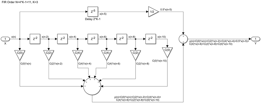
We can recognize again the same structure we have seen in the interpolator case, just connected in a slightly different way. We still have two filter branches, one a pure delay and the other one an even-symmetric single rate FIR. We already have efficient implementations for the later, so this is how a direct half-band decimator would look like for the case when N=19:

image

Note that there is no need for a final fabric post-adder, we achieve the same result by injecting the even input samples at the entry point of the adder chain, with a proper delay. A transposed implementation is of course also possible:

The transpose version is more efficient, with lower latency but limited scalability beyond about 20 taps. This problem can always be addressed by inserting extra pipeline registers. image


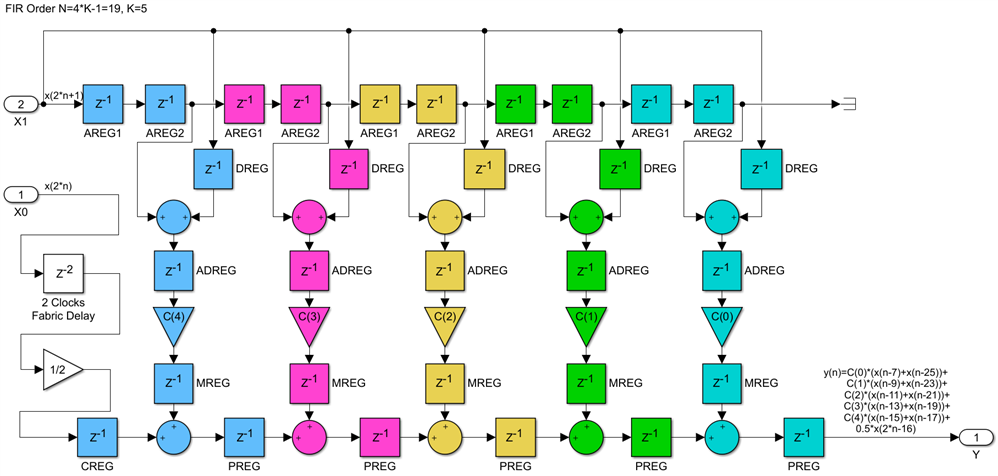
Like it was the case with the half-band interpolating FIR, a half-band decimator is 8x more efficient in terms of multiplications per output sample than the direct, naïve implementation of the mathematical algorithm. We get a 2x improvement if we take advantage of the prototype filter symmetry and another 2x factor for not computing multiplications with coefficients that are zero. Finally, since we do not need to compute output samples that we will then throw away through decimation, we have another 2x efficiency factor.


Next we will go back to single rate FIRs, where the input sample rate is equal to the output sample rate, but will consider the case when this sample rate is different from the hardware clock frequency.


Back to the top: The Art of FPGA Design Season 2

  • Sign in to reply

Top Comments

  • fpgaguru
    fpgaguru over 4 years ago +2
    Hi Rod, There are three main ways you can do DSP hardware design with FPGAs. 1. Classic HDL design flow, using either Verilog (or rather SystemVerilog) or VHDL 2. With SysGen, which requires Matlab and…
  • drozwood90
    drozwood90 over 4 years ago in reply to 14rhb +2
    Hi there, In older versions of the tools, you needed to have the HLS version installed + licensed. I would suggest that if you have a webpack supported board, upgrade to the 2020.2 tools using Vitis. There…
  • fpgaguru
    fpgaguru over 4 years ago in reply to 14rhb +2
    Hi Rod, I hope you meant 2020.2, not 2012.2. I think that Vitis/Vivado 2020.2 would be the right tool flow for you to use. Catalin
  • 14rhb
    14rhb over 4 years ago in reply to fpgaguru

    Ah, well spotted. It was indeed a typo on my part, I meant 2020.2 having started off with Vivado 2018 image

    • Cancel
    • Vote Up +1 Vote Down
    • Sign in to reply
    • More
    • Cancel
  • fpgaguru
    fpgaguru over 4 years ago in reply to 14rhb

    Hi Rod,


    I hope you meant 2020.2, not 2012.2. I think that Vitis/Vivado 2020.2 would be the right tool flow for you to use.


    Catalin

    • Cancel
    • Vote Up +2 Vote Down
    • Sign in to reply
    • More
    • Cancel
  • drozwood90
    drozwood90 over 4 years ago in reply to 14rhb

    Hi there,


    In older versions of the tools, you needed to have the HLS version installed + licensed.

    I would suggest that if you have a webpack supported board, upgrade to the 2020.2 tools using Vitis.  There you get the advantages of using HLS but the tools for the most part, handle data movers for you.


    --Dan

    • Cancel
    • Vote Up +2 Vote Down
    • Sign in to reply
    • More
    • Cancel
  • 14rhb
    14rhb over 4 years ago in reply to fpgaguru

    Hi Catalin,


    Thank you for such an insightful and well explained reply.


    To be honest my limited understanding of Vivado versions has only improved over the last few weeks since my roadtest of the Digilent USB104 board which encouraged me to look at other versions. In doing that I have now upgraded to look also at Vitis. One thing I still didn't understand was the HLS approach - my project approach used existing IP blocks to build a block design or sometimes I tried my hand at my own RTL blocks (using Verilog) to make the hardware side and then dropped to SDK to program the Microblaze core.


    My Verilog/VHDL knowledge is also limited so the first option would likely be a struggle for me. That said, in a good way as I'd be forced to learn more to get the approach to work. I think the second approach sounds good but I'm currently not in a position to afford Matlab. What would work for me though as I'm fairly familiar with C/C++ is the last approach and using HLS.


    I've currently have Vivado/Vitis 2012.2 2020.2 installed. Am I correct in my understanding, I should be able to create a RTL block using C/C++ in HLS.


    Thank you for your help image


    Edited 3rd Feb 2021 thanks to comments below: changed Vivado/Vitis 2012.2 to 2020.2

    • Cancel
    • Vote Up +1 Vote Down
    • Sign in to reply
    • More
    • Cancel
  • fpgaguru
    fpgaguru over 4 years ago

    Hi Rod,


    There are three main ways you can do DSP hardware design with FPGAs.


    1. Classic HDL design flow, using either Verilog (or rather SystemVerilog) or VHDL

    2. With SysGen, which requires Matlab and Simulink from Mathworks

    3. Using HLS, which means programming in C/C++


    All three require of course Vivado if you are targetting a Xilinx FPGA but that's free if you can live with the limited number of parts supported by the free edition. Note that there are no other limitation, the free edition is a full blown one and includes SysGen and HLS.


    The first option requires HDL design expertise. It is the best one if you want to maximize the performance of your design implementation. The second option is not free, but Mathworks provides a version of Matlab and Simulink for personal use for about $200.  Finally, the third version, which is also free, might make sense if you have software development experience with the C/C++ languages. However, you pay a price in design size and speed and you still need to have a good understanding of hardware design principles, the idea that you take some arbitrary C code, push a button and magically get an efficient FPGA implementation is still a pipe dream.


    My posts in this second season might give give you the wrong idea that you need to explicitly configure the DSP48 primitives to do DSP designs in XIlinx FPGAs, that's definitely not the case. I am going into the details of the DSP48s because the goal for this series of posts is to show how to go from a mathematical algorithm to an efficient hardware implementation, using various FIR architectures as a teaching vehicle. While understanding all these DSP48 details will do you no harm, you can still do good DSP hardware design using either one of the three flows mentioned above, without ever configuring a single DSP48 primitive. They can be inferred from behavioral HDL code or C/C++, there is a lot of free IP like FIR Compiler, FFTs and so on which you can instantiate in your HDL or in SysGen and so on.


    If you tell me which one of the three design flows is the one you are most familiar with, maybe I can make further suggestions.


    The main barrier into becoming an expert in this field is not the lack of tools, even if you insist on completely free. You can definitely get a board and tools for less than the price of a university course book. But this is not something that can be learned in a week or even a couple of months, it requires a lot of time and effort. Maybe not the proverbial 10,000 hours, but not a lot less than that either.


    Catalin

    • Cancel
    • Vote Up +2 Vote Down
    • Sign in to reply
    • More
    • Cancel
>
element14 Community

element14 is the first online community specifically for engineers. Connect with your peers and get expert answers to your questions.

  • Members
  • Learn
  • Technologies
  • Challenges & Projects
  • Products
  • Store
  • About Us
  • Feedback & Support
  • FAQs
  • Terms of Use
  • Privacy Policy
  • Legal and Copyright Notices
  • Sitemap
  • Cookies

An Avnet Company © 2025 Premier Farnell Limited. All Rights Reserved.

Premier Farnell Ltd, registered in England and Wales (no 00876412), registered office: Farnell House, Forge Lane, Leeds LS12 2NE.

ICP 备案号 10220084.

Follow element14

  • X
  • Facebook
  • linkedin
  • YouTube