


Multichannel and Overclocking FIRs - The Single Rate non-Symmetric Case
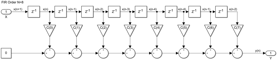
We are looking now at the case of the single rate FIR filter where the sample rate is a sub-multiple of the FPGA clock rate. For example, let's say that the input and output sample rates of our single rate FIR of order N=8 are 200Msps, but we know we can run our FPGA DSP48s and fabric at 800MHz. We can take advantage of the extra FPGA speed in two ways. We can either implement four such filters for the price of one, that is using the same 8 DSP48s, or we can implement a single filter with only two DSP48s, M=4 times less resources, where M is the ratio between the fabric clock rate and the data sample rate. In both cases we start from the same mathematical model, a direct form, single rate non-symmetric FIR of order N=8:
The first case in which we implement four filters, in fact a filter with four channels which are time division multiplexed, is the easier one. We simply replace each delay in the single channel design with M delays:
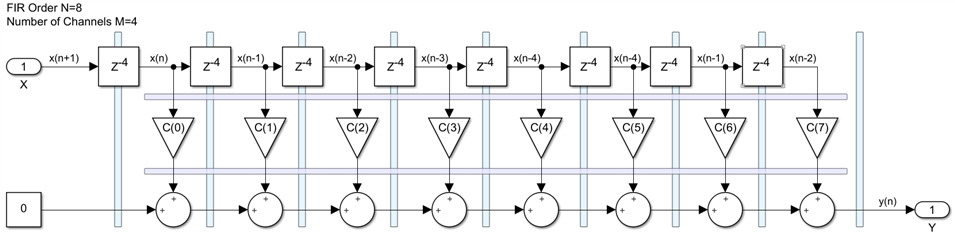
We then pipeline this design using longitudinal and transversal pipeline cuts and we arrive at an efficient high sped and scalable implementation:
Like in previous posts, the resources that will fit inside each DSP48 are colored with the same background color and fabric resources have a white background. This structure is generic and scalable, a multi channel FIR of any order N and number of channels M can be built using this scheme and will still run at the maximum possible system clock frequency.
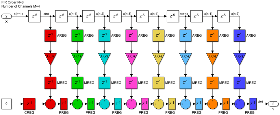
The second case, where we only need one channel but we want to reduce the resource utilization by a factor of M, is more complicated. The basic idea is that we will use one DSP48 to implement M filter taps in M consecutive clock cycles. The DSP48 multiplier will multiply M consecutive samples with different coefficient values, which will have to be stored in a ROM look-up table, while the DSP48 post adder will have to implement an accumulator which will add together the M partial products sequentially and then all these partial sums will have to be added together. Something like this:

The problem with this scheme is that there are M+1 adders in each sub-block, but we have only one adder and M clocks to do all the additions. The key observation is that the first adder in each sub-chain is not really needed because it adds the first partial product with a zero constant. So we could rearrange the adders like this to require only M additions every M clocks.
But this still leaves us with another issue. The partial sum coming from the upstream sub-block will be available in clock M-1, however, the next block downstream needs it in clock 0, to add it with the first partial product, because in the next M-1 clocks the adder must be used as an accumulator for each new partial product. The input delay line will be broken into sections of M delays and a new sample will be pushed into these registers only once every M clocks as indicated by the valid data input port DVI. A multiplexer selects every sample in this delay line for M consecutive clocks, which is then multiplied with a different coefficient read from a ROM table. The data multiplexer and the coefficient ROM are both addressed by the same counter, which counts continuously from 0 to M-1. To keep the counter in sync with the data being shifted in, the DVI signal is also used as a synchronous reset for the address counter. The partial products are accumulated with an accumulator built with an adder and a register. For M-1 clocks, the accumulator will add a new product to the partial sum. For one clock, however, the value coming from the upstream accumulator is added with the first product of a set of M, which is also controlled by the DVI signal.
The problem mentioned earlier is solved by delaying the shift register data and the data valid signal from one block to the next by M-1 clocks. So the DVI of the downstream block is active M-1 clocks after the DVI of the block upstream of it. To avoid using M-1 registers for the data we use a clock enabled register to capture to proper value to be sent from one block to the next. It is a single register, but that sample is in fact delayed by M-1 clocks:

This is a much more complicated design, but it still does what the original filter did, except that it requires M clocks instead of one to compute an output sample but using M times fewer multipliers and adders, so you might need to think about this for a bit. The next step is to pipeline this design structure, which is called an overclocked implementation or a semi-parallel one. We do this using pipeline cuts, in this case three longitudinal ones and a transversal one for every DSP48. After inserting all these registers and doing some rearrangement using register pushing we arrive at the following implementation:

Once again, the blocks are colored based on the DSP48 they belong to. To achieve the highest possible clock rate, the addressable shift register mux and the coefficient ROM both have their own pipeline registers. Every fabric LUT6 has two FF associated with it and can hold either two coefficient bits or two data bits. For this reason, the resources going into the same fabric slices are also colored with the same background color.
This structure too is also very efficient, generic and scalable to any N and M combination. For the case where N is not divisible by M, the filter coefficients must be zero padded until the new filter order becomes a multiple of M.
Back to the top: The Art of FPGA Design Season 2