


Implementing the First and Second Order All Pass Sections with DSP Primitives
We are almost there now. We have the LWDF IIR filter architecture, which is much better then the classic biquad cascade:
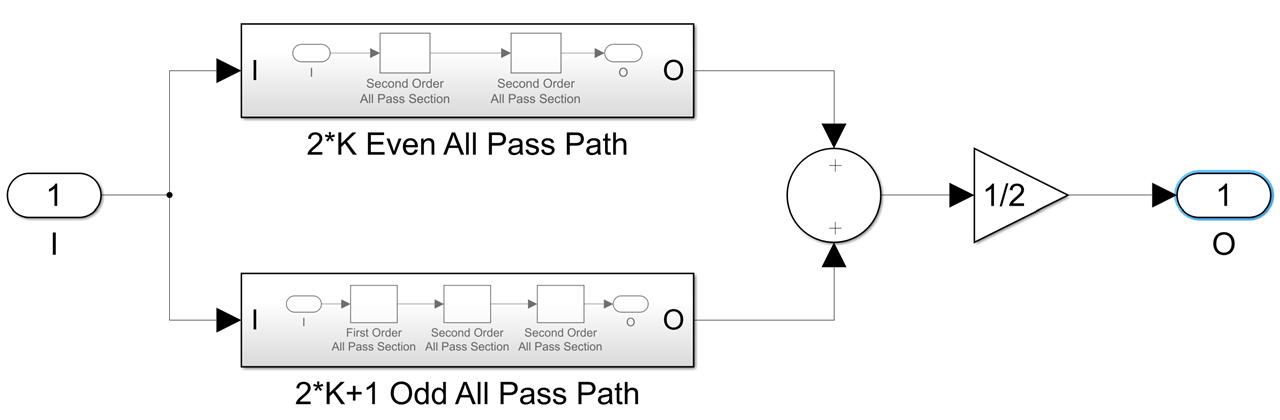
It is made out of two parallel all pass paths, each one a cascade of first and second order all pass sections, for which we have an architecture that minimizes the number of multipliers and adders and should map well into one respectively two DSPs:
And we have an algorithm that calculates the filter order N and all the coefficients based on a set of transfer function specifications, for four different types of IIR filters - Butterworth, Chebyshev I and II and Elliptic, both normal and bireciprocal. For the bireciprocal case the filter structure is exactly the same, we simply set c respectively c1 to zero.
What is needed now is an efficient mapping of the first and second order all pass sections into one, respectively two DSP primitives. For FIR filters I used the techniques of pipeline cuts and register pushing, see Post 4, with great success. Unfortunately, that will not work for IIR filters - both first and second order sections have tight feedback loops with only one delay in that loop, while the FIRs had no such thing. The number of delays in a feedback loop is invariant and no amount of pipeline cutting and register pushing can change that.
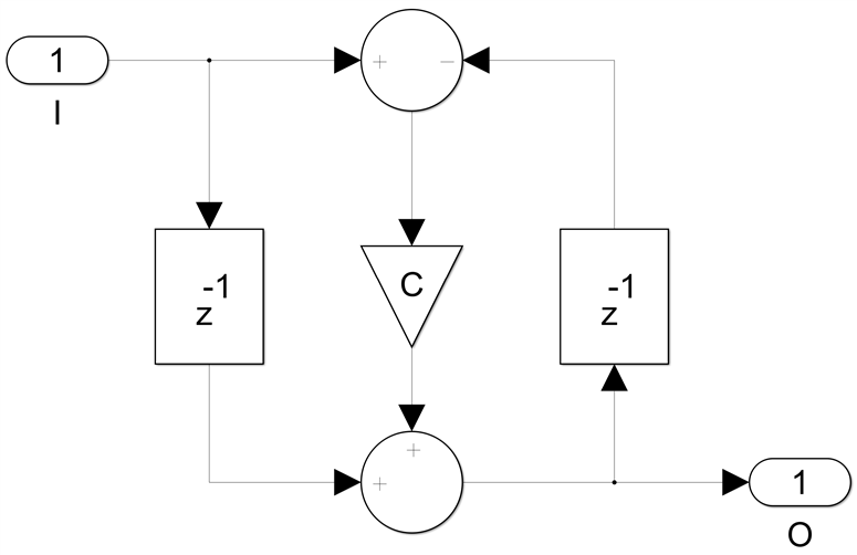
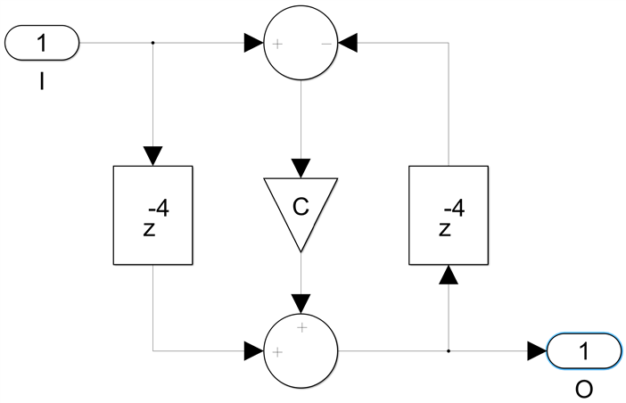
While we can map the first section all pass into a single DSP primitive like this:
this underpipelined configuration will be quite slow, achieving maybe 250MHz while clocks up to 1GHz are possible with a fully pipelined DSP, which requires four pipeline levels, AREG and DREG at the input of the preadder, ADREG after the preadder, MREG for the multiplier and PREG at the output of the postadder.
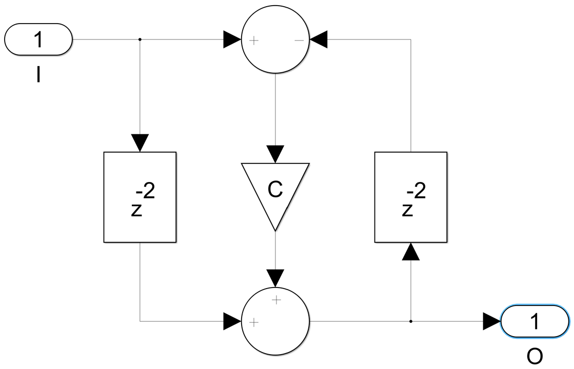
What we can do is replace each delay in the original diagram by four delays:
If we look at this as a 4-channel implementation, with TDM interleaved input and output samples, this is functionally equivalent to the original but with four channels instead of a single one. Even if we manage to run this at 1GHz, we have not increased the sample rate at all, it is still 250Msps, but we get four all pass sections for the price of one - we have not increased the sample rate, but we have improved the device utilization efficiency by 4x. We can use this to build four IIR filters for the price of one, or with the addition of a simple mux and looping the output back into the input we can implement a single chain of four all pass sections with the resources of just one. With four delays in the feedback loop we can now start pushing registers and we get this very efficient implementation:
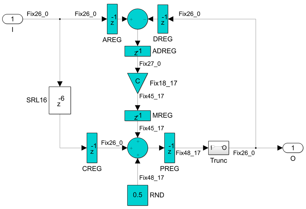
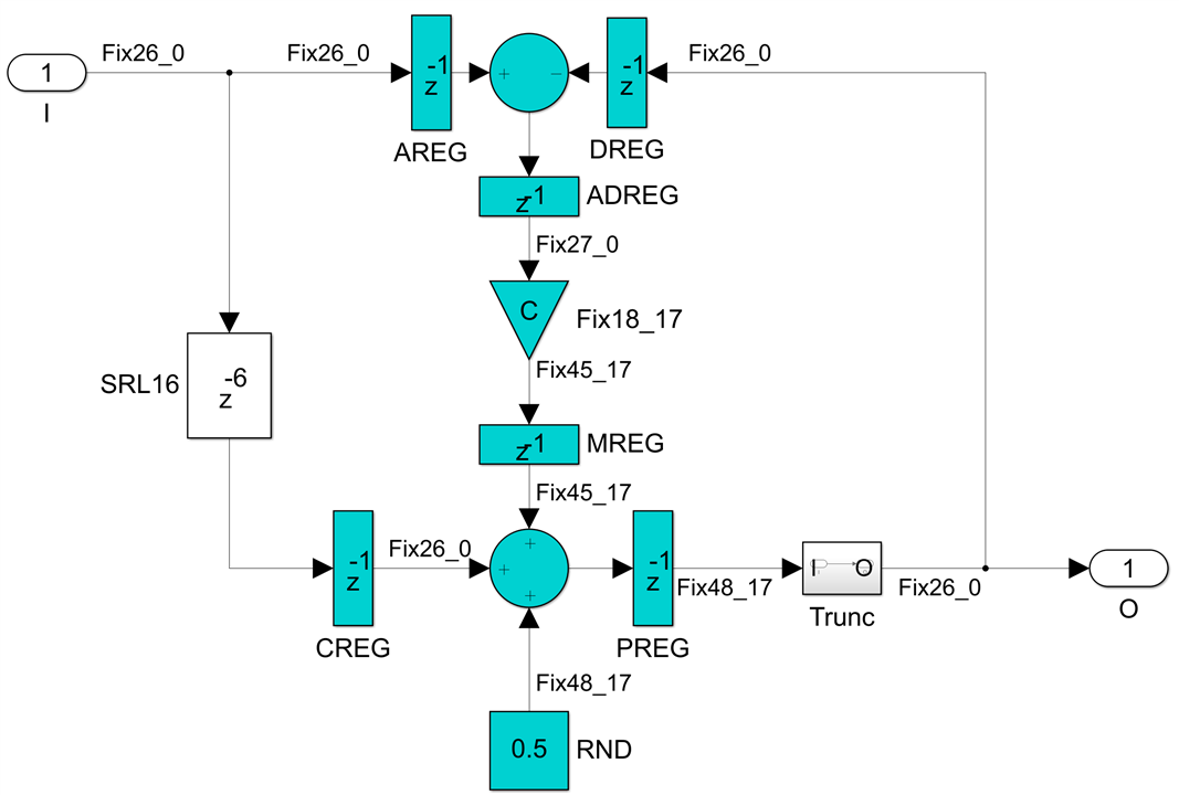
While the total latency has increased by four clocks, this is still functionally equivalent to the original. The DSP48E2 (I assumed an UltraScale+ FPGA family target) is now fully pipelined and will run at the maximum data sheet speed, 891MHz in a -3 speed grade in this case. In Versal FPGAs speeds up to 1150MHz are possible. The fixed point data type format convention I used here is FixN_M, meaning N-bit signed fixed point numbers with M fractional bits to the right of the binary point. The DSP48E2 has a 27-bit preadder, a 27x18 signed multiplier and a 48-bit post adder so the largest possible bit range for the all pass section input and output samples is 26 bits, to handle the 1 bit growth in the preadder. 18 bits are more than enough precision for the filter coefficients, while the internal multiplication and postadder operations are done with the extra fractional 17 bits to maintain precision and the result is rounded back to 26 bits by adding 0.5 and then truncating away the fractional bits, this way the rounding operation is essentially free.
Implementing a first order all pas section with 26-bit data and 18-bit coefficient bit ranges requires a single DSP primitive and one SRL16 shift register delay, which is just 13 LUT6es and 26 FFs. The maximum sample rate that can be achieved is a quarter of the clock frequency, so 222.75Msps, but we get four instances running in parallel at this rate with a single DSP48E2 clocked at 891MHz. So we get an average maximum sample rate but 100% DSP utilization efficiency.
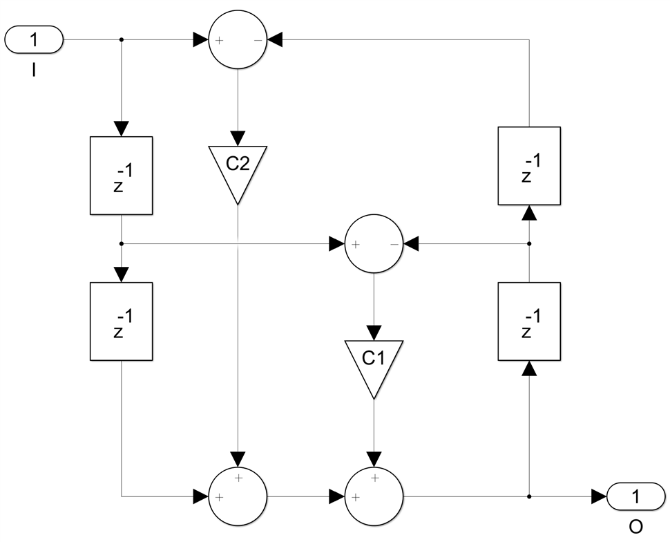
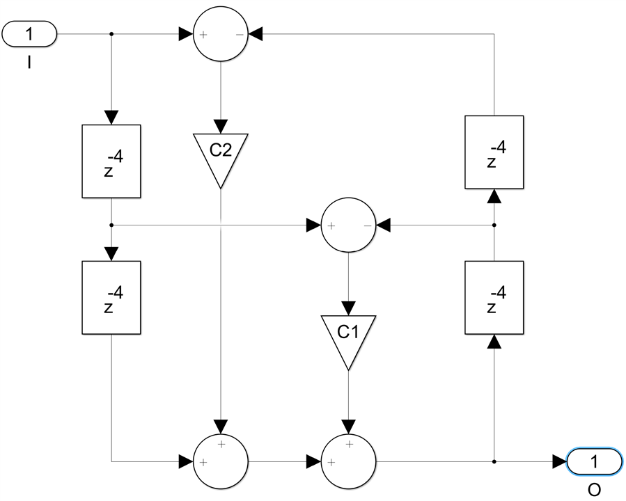
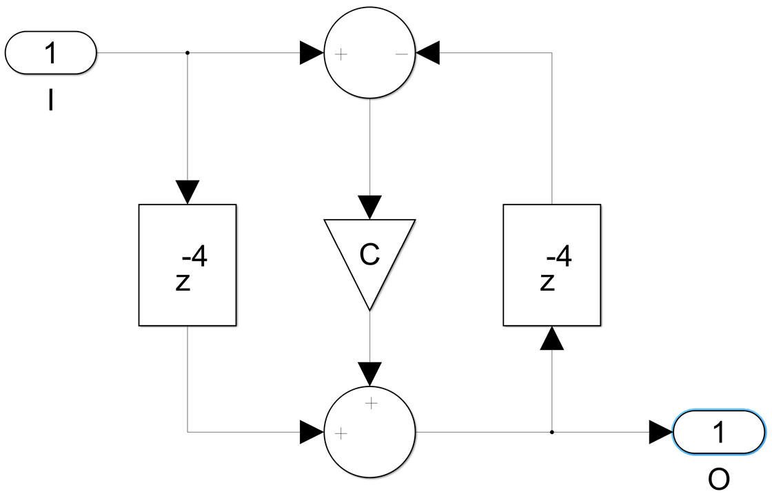
The same thing can be done for the second order section, we first replace each delay with four delays:
then we do the register pushing and fully pipeline the two DSP48E2s:
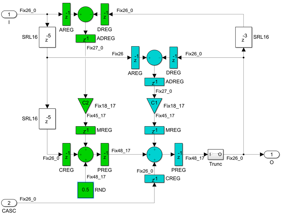
The result is very similar, two fully pipelined DSP primitives connected with the P cascade, with the same 26-bit data, 18-bit coefficients and rounding through adding 0.5 and then truncating. The increase in latency is now 5 clocks. Three SRL16 delay lines are needed, so 39 LUT6es and 78 FFs. We also get an optional cascade input port, which can be used on the last second order section of the even branch to implement the LWDF filter final add and divide by 2 operation, also for free.
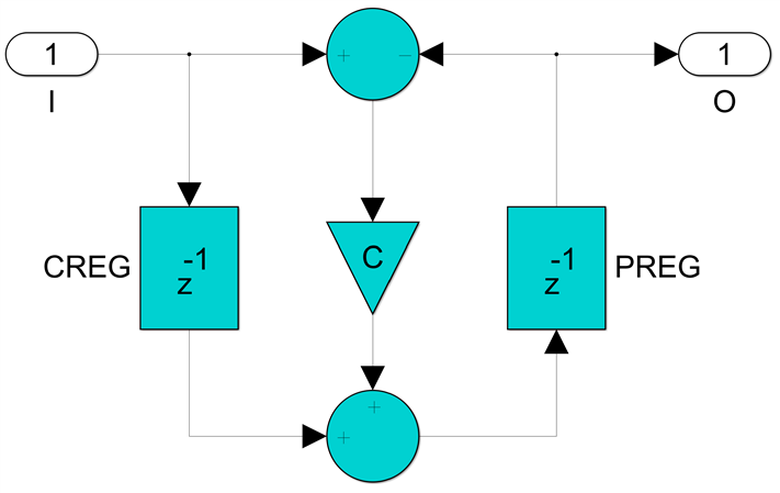
Finally, we have the bireciprocal case to consider. The general structure of the LWDF filter is exactly the same in this case, except the first order section with a coefficient c=0 becomes simply a delay, while the second order one with c(1)=0 now looks like this:
We only need a packing factor of two now to achieve four delays in the feedback loop, giving us two channels running at a sample rate equal to half the clock frequency:
The pipelined DSP48E2 implementation is now:
which is absolutely identical to the pipelined first order section, except that now we have two channels running at 445.5Msps. So we do not need a different module for the bireciprocal case, the bireciprocal second order building block is identical to the normal single order one, while the first order bireciprocal all pass section is simply a delay.
As long as we are OK with only running at a sample rate that is a quarter of the clock rate (or half in the bireciprocal case) but getting four (respectively two) filters for the price of one and with the inherent non-linear phase that is the nature of all IIR filters, this is an excellent solution, really compact and as efficient as the FIR implementations I presented in earlier posts, but using a lot less DSP resources.
I could say now that this concludes the topic of implementing LWDF IIR filters in AMD/Xilinx FPGAs but there is so much more to this story. For example, some LWDF IIR filter design examples and comparisons with equivalent FIR filters would be nice - what kind of utilization and power savings are possible? Or what if we really need sample rates equal to the clock frequency, not just a quarter or half? Are multiplierless IIR filters possible and what kind of performance can they achieve? And what about the promised three different ways of achieving linear phase with IIR filters?
So please stay tuned, there is much more to come.
Back to the top: The Art of FPGA Design Season 2