I'm trying to write i2c code for Zynq, in VHDL.
I have difficulties creating a TRI-STATE pin.
The output logic should be: the pin is either pulled down to 0, or open-collector.
I have a pull-up resistor between that pin and VCC (3.3 V).
I'm expecting that if I write '0', it is low. When I write 'Z', it's open collector and pulled high by my pullup.
But in my design, the pin stays low. 0.62 V.
I thought, from reading up, that I should be done by:
- defining the pin as INOUT
- when you want to drive it low, assign '0'.
- when you want to drive it open collector, assign 'Z'.
- put an external pullup between pin and VCC
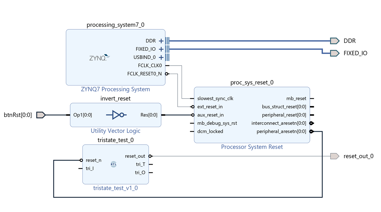
I created a testbed that puts the pin in "Z' mode, except when reset is asserted (via an external button).
In my testbed I also added a test pin, that I attach to an LED, that is high when the reset is asserted.
I connected a multimeter to the output.
The LED behaves as expected. It lights up when I assert the reset.
But the tri-state pin stays low, whether I write '0' or 'Z' to it.
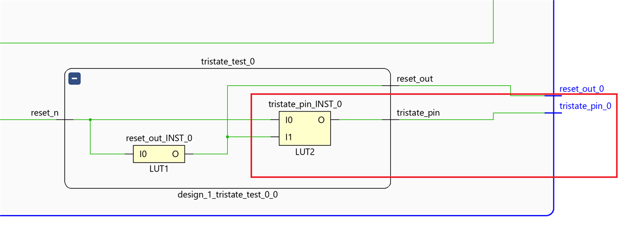
entity tristate_test is
Port (
reset_n: in std_logic;
reset_out: out std_logic;
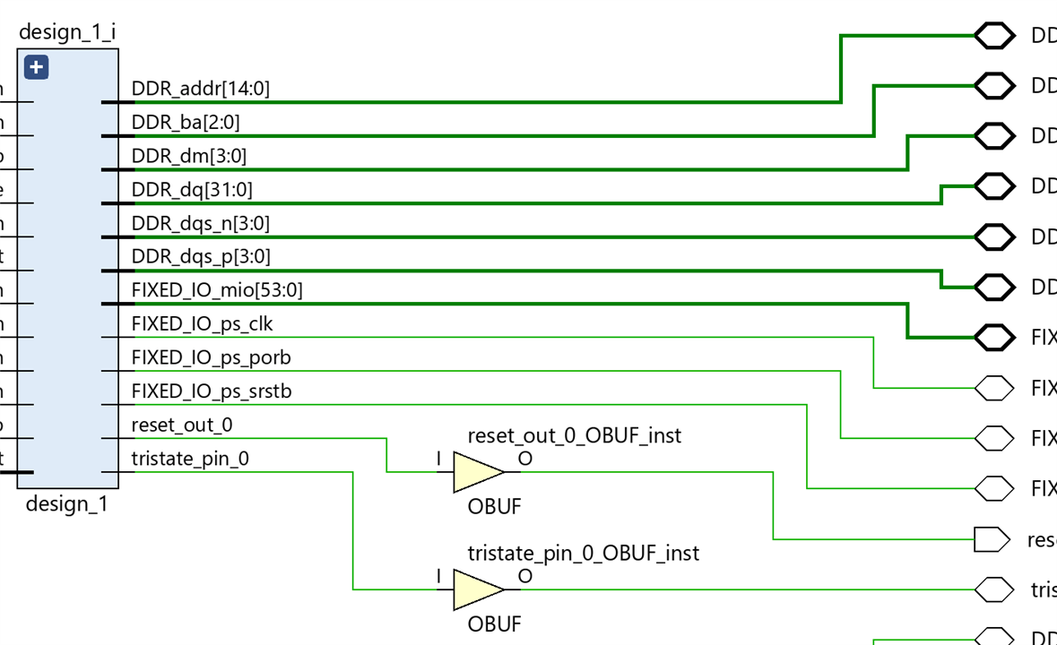
tristate_pin : inout std_logic);
end tristate_test;
architecture Behavioral of tristate_test is
begin
reset_active: process (reset_n) is
begin
if (reset_n = '0') then
tristate_pin <= '0';
reset_out <= '1';
else
tristate_pin <= 'Z';
reset_out <= '0';
end if;
end process reset_active;
end Behavioral;
Here is how I set the constraint:
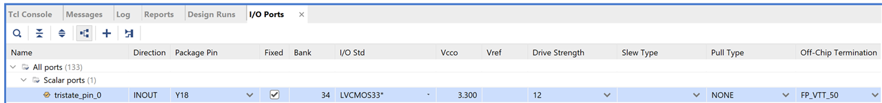
set_property PACKAGE_PIN Y18 [get_ports tristate_pin_0]
set_property IOSTANDARD LVCMOS33 [get_ports tristate_pin_0]
set_property DRIVE 12 [get_ports tristate_pin_0]
Schema:

PMOD A pin 1 is PACKAGE_PIN Y18
What am I doing wrong?