


In the past few postings, I’ve covered the contents of the kit, showed you how I soldered the WL-ICLEDs to the Adafruit breakouts, achieved “first light” using FastLED and did some PCB and 3D printing design. In the last chapter, I ended the post with polls asking whether you thought the PCBs would arrive in time and whether you thought I could solder the remaining types of LEDs using my hot-air-gun technique.
In this post, we’ll find out the answers to those questions ...
One PCB Arrives
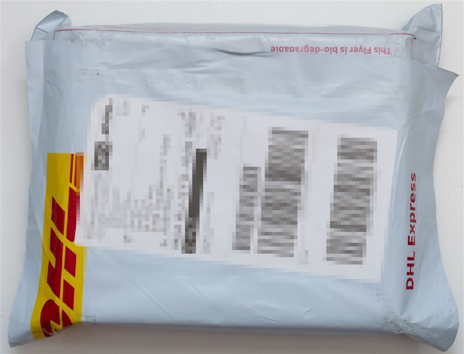
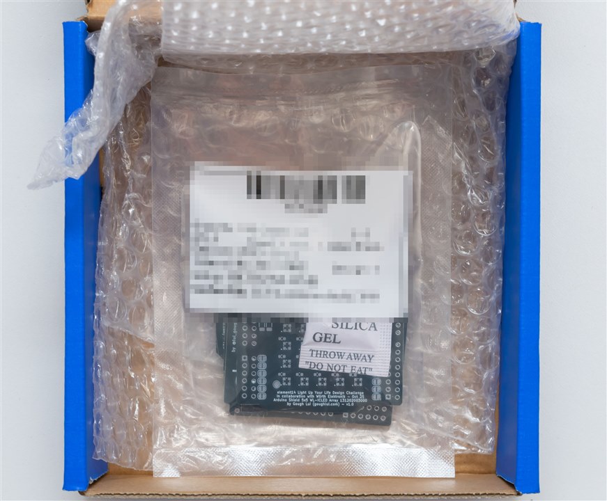
This week, I received my first parcel. Thanks to the modern miracle of express couriers such as DHL, which take advantage of air transport and logistics, and the streamlined processes of Chinese manufacturers such as JLCPCB, it was just under a week from uploading my files to receiving this parcel on my doorstep. It did come at a price though – about AU$22 more than the “economic” shipping option so that’s about the cost of a lunch meal here. It was a choice I made to ensure that it would arrive before the due date – but now that the challenge has been extended by two weeks, economic shipping may have been enough.
Arrgh. It’s happened again! This box arrived upside down … a common issue in Australia. But alas, thankfully, this is something that’s recoverable.
Thankfully, as it was well packed, the boards survived their upside-down journey.
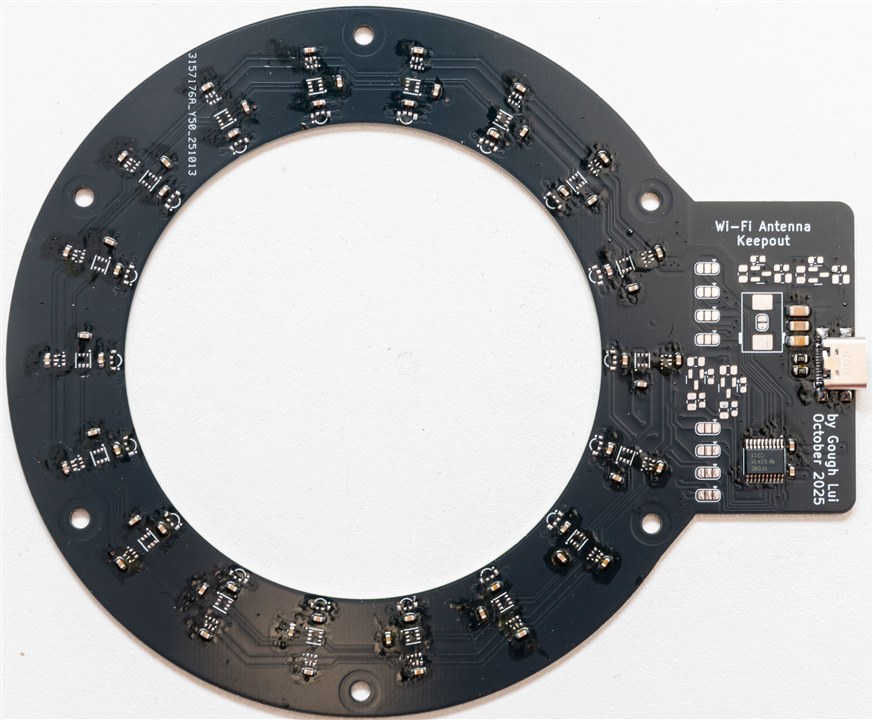
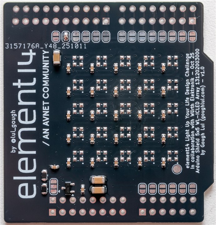
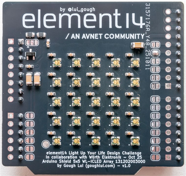
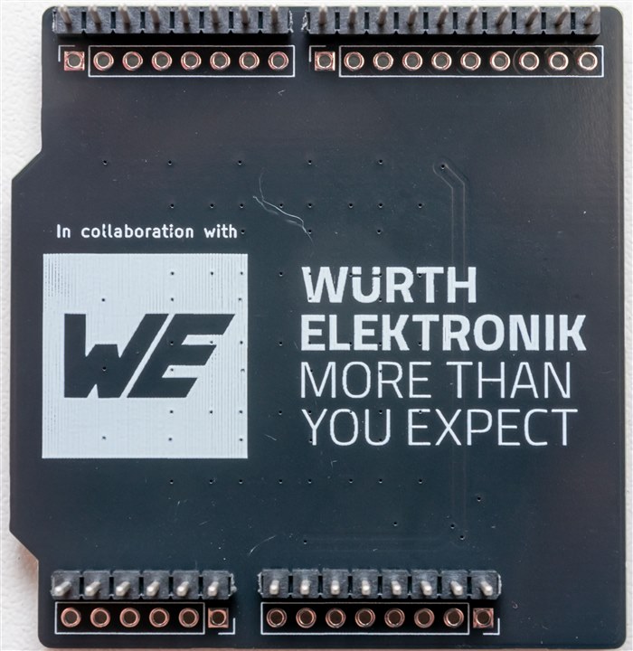
The PCB is the main PCB and I’ve got five of them as that was the minimum order quantity. What I’ll do with the remaining four, I have no idea!
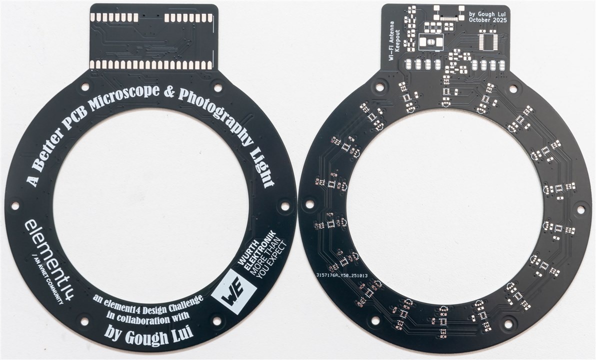
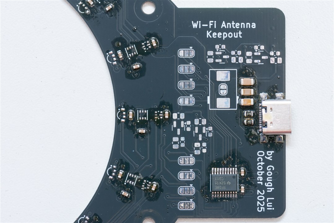
The black solder mask was a bit glossier than I had originally anticipated, but it was purposely chosen to avoid reflecting stray light, rather than maximising output with a white solder mask as other LED projects may use. You can see the silkscreen graphics are quite nice – what a shame much of it will be covered once the whole thing is assembled.
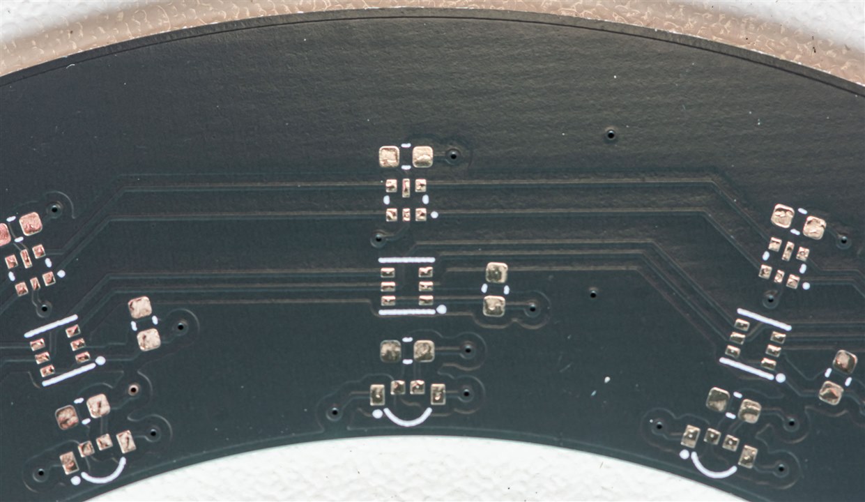
Only after handling the board in-person, did the soldering challenge become truly apparent to me.
My Secrets to Assembly
It’s a common understanding that chef’s keep secrets – things that are unwritten that can totally change the result. But rather than keep secrets, the assembly of this board allows me a chance to share some of my “secrets” which, to some, may not be secrets at all. Since videos are not particularly accessible and I needed every possible chance to succeed, I decided not to have the cameras rolling as I assembled the boards, instead, snapping photos along the way.
Secret #1 – What’s your flux?
While I’ve noted that lower melting point solders to be preferable for SMD rework as it reduces temperature requirements and stress on the board, the choice of flux is important too.
The vast majority of low-cost hobby solders seem to be some form of rosin, with a common designation of RMA (rosin, mildly activated). These are, as far as I understand, derived from tree-sap and have a sort of “woody” scent that was the smell of electronics when I was younger. These solders often leave yellowish sticky or hard residues. The industry has moved, in part, and now it seems no-clean solders which have less active fluxes and clear residues are most popular. These result in visually attractive boards but unfortunately, result in residues that are difficult to clear (often requiring special cleaning liquids or scrubbing with IPA).
While those are perhaps the more common fluxes amongst hobbyists, I think those fluxes could be setting you up for trouble. Part of the reason is the viscous nature of these fluxes, which can result in a somewhat “gel” like substance being left on the board (especially in the case of excess flux) upon which SMD components may be tempted to “float” on top of. Thus, getting a good joint can be more tricky. Things get even worse if you didn’t pay attention and start mixing incompatible fluxes because your flux pen is one type and your solder wire is a different type.
Instead, I’ve settled on the use of water-soluble fluxes instead. These fluxes are somewhat more “flowy” and liquid in nature, but best of all, they are easily removed and cleaned with warm-to-hot water (which is easily accessible). I find it to be easier to work with as I can stop and clean off the board to prevent stale, sticky flux accumulation in multi-step soldering. But it’s not quite all positives – the flux smokes and smells pretty horrible (a bit like cat urine) so an extraction system is highly recommended. Thorough cleaning is also MANDATORY. Failure to clean will lead to corrosion over time that eats away at traces and damages the solder joint, leading to failure. In an industrial operational context, cleaning usually entails washing while monitoring the ion concentration in the washing water until it reaches a particular threshold – but for home use, I tend to wash three times (and until the water becomes normal – e.g. no bubbling foam, no grey appearance).
At this time, I’m using a mixture of Loctite Multicore solder with Hydro-X flux and a Kester 2331-ZX flux pen and it’s a combination that’s worked well for the past few years for me. I love to add flux to “freshen” up solder when soldering in multiple waves, ensure good wetting and provide a medium to allow heat to flow between board and component.
Secret #2 – It’s all in the tweezers!
The next part of working with SMD components is being able to handle them. The human pick-and-place will find it difficult to do it with just bare fingers alone, so tweezers are mandatory. But the type of tweezers is very important to ensuring you can pick up the components comfortably without the risk of them pinging out randomly across the lab and resulting in the need to launch a search party.
I didn’t appreciate just how important this was until I got some decent tweezers. A good set of tweezers have nice and fine tips that line-up with one another perfectly and refuse to “twist” or misregister with their opposing tip. More than this, they would be made of a relatively robust material so they do not bend or warp and are easy to clean, are chemical and heat resistant. It should be ESD-safe as well, for handling semiconductor components.
After my review of the Weller WXsmart, I fell in love with the Weller Erem E3CSA tweezers that were part of the kit. It was everything a good tweezer should be and it made positioning components a breeze. The rubberised handle proved to be good to insulate the heat but also ensure operator comfort. But I also know that spending AU$100 or so on a pair of tweezers may sound crazy for hobbyists.
For a more affordable option, I came across the Japanese-made Engineer PT-16 solid-arm tweezers. The solid arms keep the tips in good registration and add a nice amount of weight to the tweezers, making them a delight to handle, especially as they can be found for a more affordable AU$25. It’s not the cheapest, and you will sacrifice the rubberised handle, but it will pay for itself in saved frustration compared to ordinary generic tweezers.
Secret #3 – Soldering order
When constructing electronic kits of the through-hole variety, often you sequence the components you fit by their height to ensure that it’s easier to populate the PCB. But when it comes to SMD, I tend to consider heat tolerance and location to plan my soldering. Soldering a fresh board is also completely different from repairing an existing board where other components may already be populated.
The first thing is that I will most often design SMD boards with just a single side populated. This makes it easier to hand populate at home as there is no risk of components falling off the board and/or heat damage to components on the opposite side of the board. Another key design choice I will make is to ensure the largest copper planes possible on both sides of the board, as having the copper present helps conduct the heat around, avoiding the hot air from impinging directly on the fibreglass substrate which can easily burn when exposed to soldering-level temperatures for long times. This is especially the case as hot air guns do not always have air at a uniform temperature depending on their design – there can be hot and cold spots in the “jet” of air.
Components such as plastic package ICs, ceramic capacitors, resistors and inductors generally can handle more heat, so they can be soldered with hot air on the same side. If it is a fresh board with no other components, I will usually prepare the board by tinning the pads which will be used and then mounting all of the ICs, ceramic capacitors, resistors and inductors with hot air “from the top” flowing onto the component directly. If the components have excessive moisture, they could crack or become damaged, so ramping up the hot air may be a good idea.
Components such as LEDs that have clear plastic lenses or connectors with plastic formers or bodies are particularly sensitive to heat, so I tend to prepare them into place for a second wave of soldering, but this time, heating the board from the underside so that hot air does not directly impinge on the component. This prevents the component from melting, but it does mean a slower process as it takes time for heat to conduct from the rear side to the front. It is necessary to wave the heat gun around to avoid overheating one particular location, to avoid destroying the silkscreen and solder mask or causing delamination of the copper from the substrate.
Some components, like SMD electrolytic capacitors, I really don’t recommend using hot air for at all. These are high thermal mass components, which can be difficult to raise to the right temperature but also, may not be able to handle long-term heating. I’ve had one of these “explode” and vent during a hot-air-gun desoldering exercise, so I’ve learned to avoid heating boards that have these fitted. Instead, if soldering them down, use a soldering iron and go one pin at a time. If removing them from the board, cut them off as best as possible and desolder the remnants.
Secret #4 – Set your temperature, use your eyes and nose
It’s often necessary to set temperatures higher than what might be seen in datasheets for reflow soldering (e.g. 260 degrees Celsius) as the air loses temperature as it travels towards the board, and even more if it’s going to heat the opposite side of the board. While using higher temperatures increases the risk of damage – you can also damage components with lower temperatures held for too long, so it takes a bit of trial-and-error to determine which settings work best for you. I tend to gravitate around 320 degrees Celsius using my Tenma (Atten-rebadged) hot-air soldering station.
How I tend to know when I’ve got the right temperature is to use my senses. Watch the flux start to smoke and bubble, the solder liquify and wick up component legs, the “wiggle” of a component “snapping” into position due to the surface tension of the solder and the “jiggle” of a component being prodded by tweezers that’s being connected well to molten solder from all sides. If you’re not so good at this, using a thermal camera could certainly help confirm that your component is reaching sufficient temperatures to be properly soldered.
What you don’t want to smell is the smell of charred fibreglass. Burnt PCB substrate is a particularly irritating smell that you’ll find hard to get out of your nostrils.
Assembly, Step by Step
So let me show you how I put those “secrets” into practice. From a fresh board, the first step I do is tin the pads where the heat-tolerant components are to be fitted.
This is because I don’t use solder paste and I don’t order a stencil either. Instead, my method is depending on the solder mask and the geometry of the pads to just “hold” enough solder to make the connection. This works for a range of SMD sizes – but won’t necessarily work for very fine pitch (<0.4mm) which may have insufficient solder and exposed paddles or very large component pads which might get too much solder. In-between seems to work just fine.
After tinning, the remnant water-soluble flux from the solder wire is left on the board. It looks somewhat bad, but it’s a tolerable amount of residue.
I then go over all of the connection points with my flux pen to add fresh flux and hand-pick and place parts into their approximate position. As these are heat-tolerant components, I can heat-gun directly from the top.
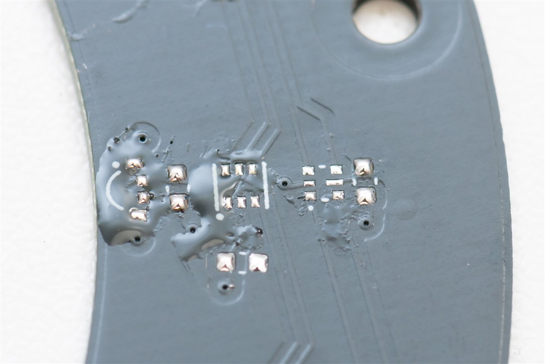
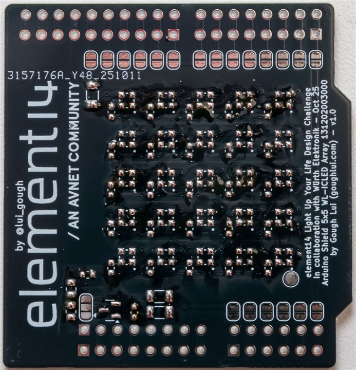
After this, the capacitors, resistors and level shifters are fitted just fine. I ran a second cycle for the USB-C connector, but heating from the underside, as this is a heavy thermal mass part which requires a bit more heat and I didn’t want the other more sensitive components to suffer. The result is a partially populated board with a notable amount of flux residue.
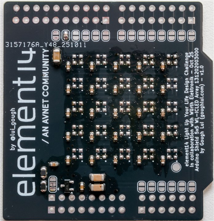
It looks dirty, but this is where the magic of water-soluble fluxes come into being. Taking the PCB to my sink, I shove it into a bucket of warm water and agitate it, refreshing the water several times over. Then, I take the board out, give it a good hit with a battery operated air duster to “push” off all the water droplets and then leave it on the bench with a fan pointed at it for a couple of hours to dry out.
It’s not quite perfect – there’s still some residue near the USB-C connector but it’s much cleaner. Removing the old flux is necessary because the flux becomes more viscous and less active – leaving it on the board when populating the LEDs makes it more difficult as the flux might “float” the LED and not allow the solder joints to make.
Clean footprints ready for soldering the LEDs. As they are sensitive, they must be done in one or two goes at the most. As a result, I went over the pads with the flux pen, populated all three types at the same time and hot-air gunned from the underside to secure them into place.
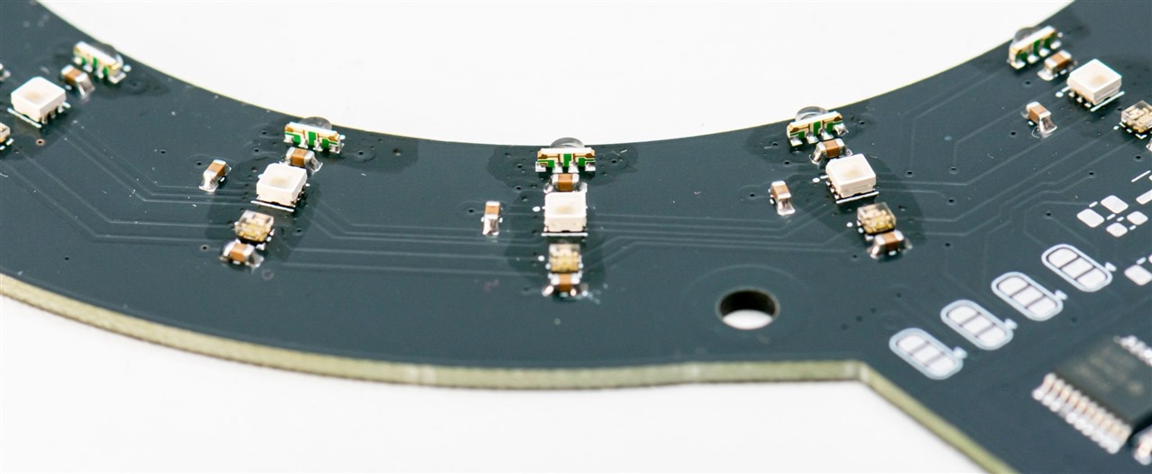
Looking good – those LEDs will “shimmy” into place as the solder liquefies and as long as it looks well aligned with the footprint, there’s no reason to intervene.
If they’re not quite in the right place, you can give it a gentle tiny nudge with a pair of tweezers on the base of the LEDs – never touch the lens though, as that can get soft and separate from the LED, damaging it permanently as it might tear off the bond wires and dies, not to mention altering the optical properties.
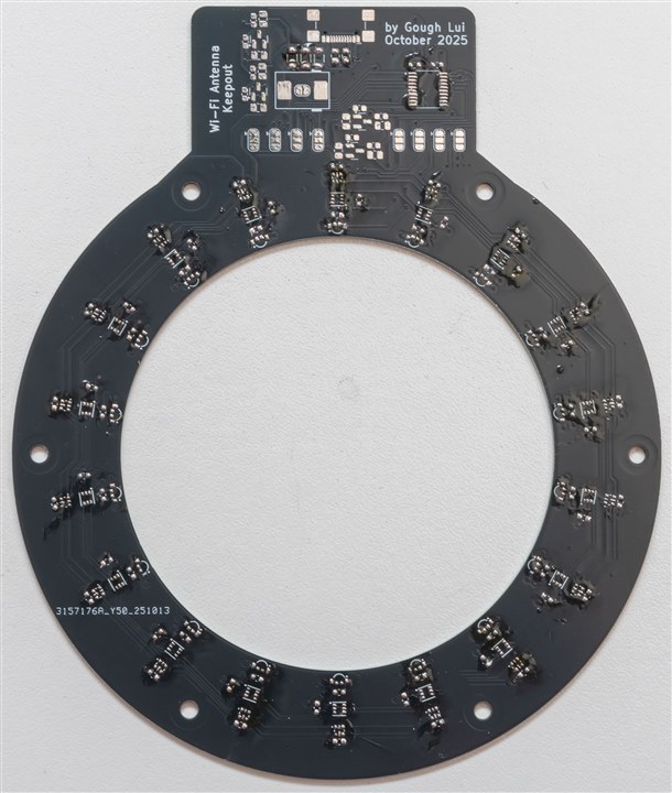
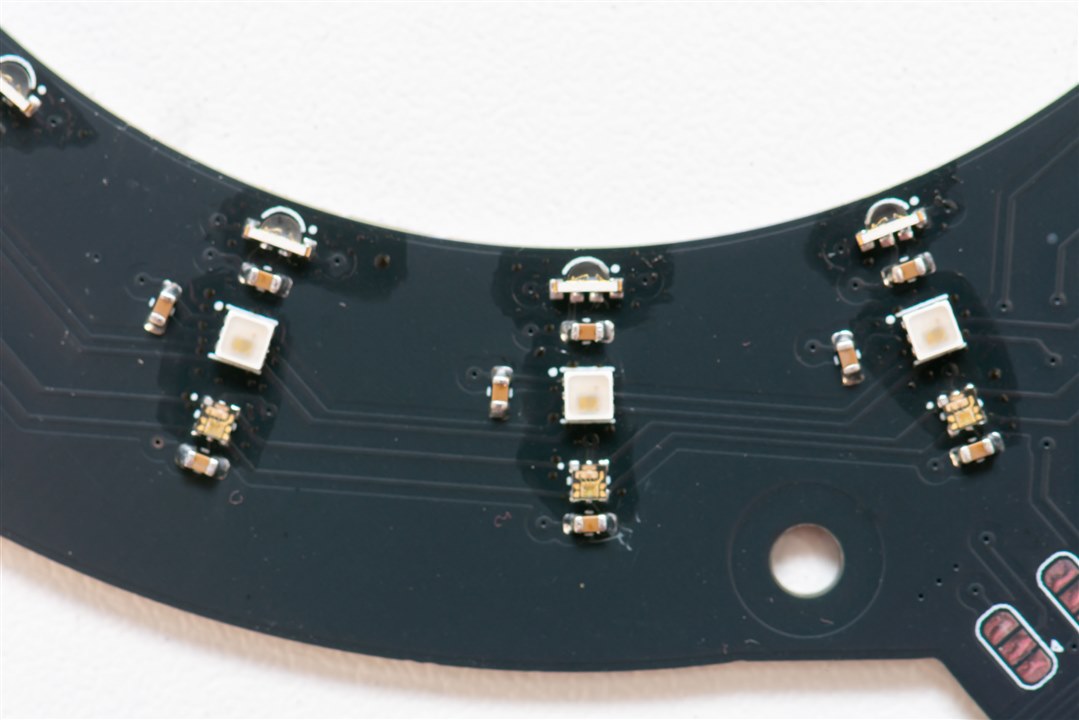
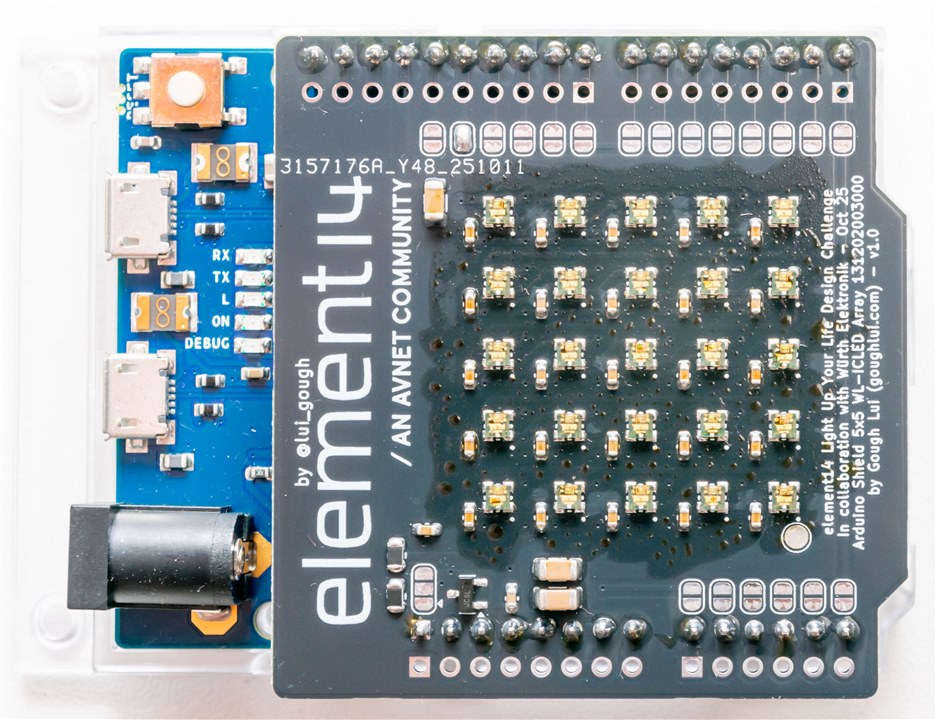
Now that all of the components on the main side are populated, I can hand-solder the castellated Raspberry Pi Pico W module to the back side with a soldering iron. This order of population avoids stress to the Pico W and conflicts where components on the underside might be damaged by heat or restricts your ability to heat from the underside.
One of the main outcomes was no damage to the solder mask or the silkscreen – overheating the rear side of the PCB is a possibility for those not careful in their hot air gun control. This would usually result in discolouration to charring and delamination.
Another PCB Arrives
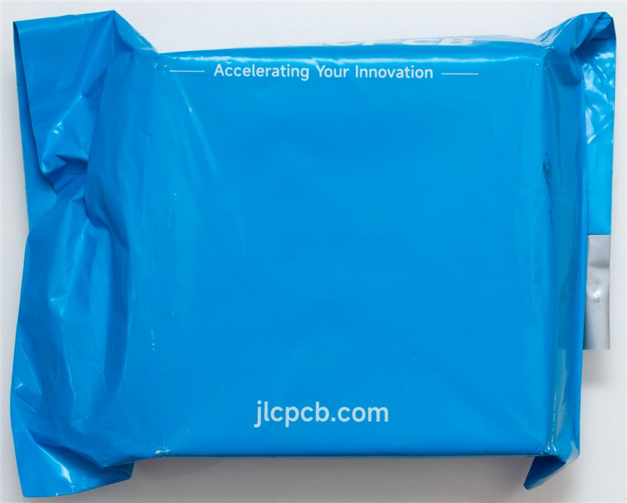
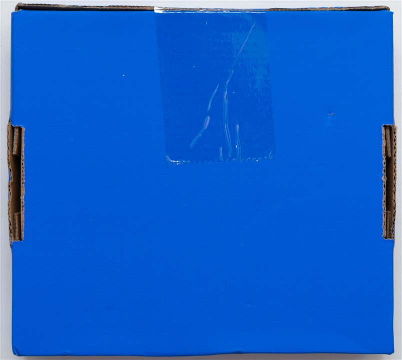
The second package arrived, also upside down at least on the outside. This parcel took about five more days (considering it was an order that was submitted earlier and arrived later), but the total cost for this one was only about AU$6.50 for the boards and postage combined. Very affordable!

Not only was the postage economical, but the box they used seemed to be a bit economical too with their logo offset from centre.
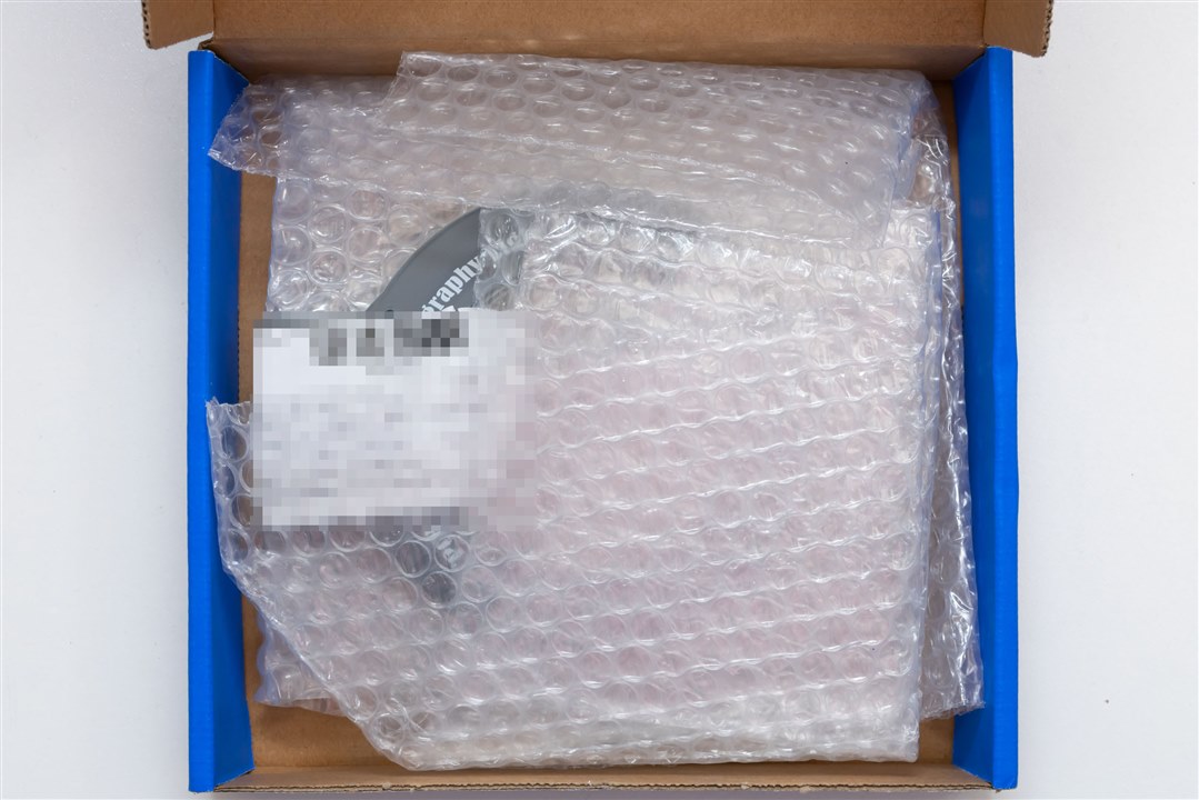
Another five boards, but I’ll only really need one of them.
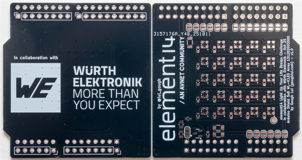
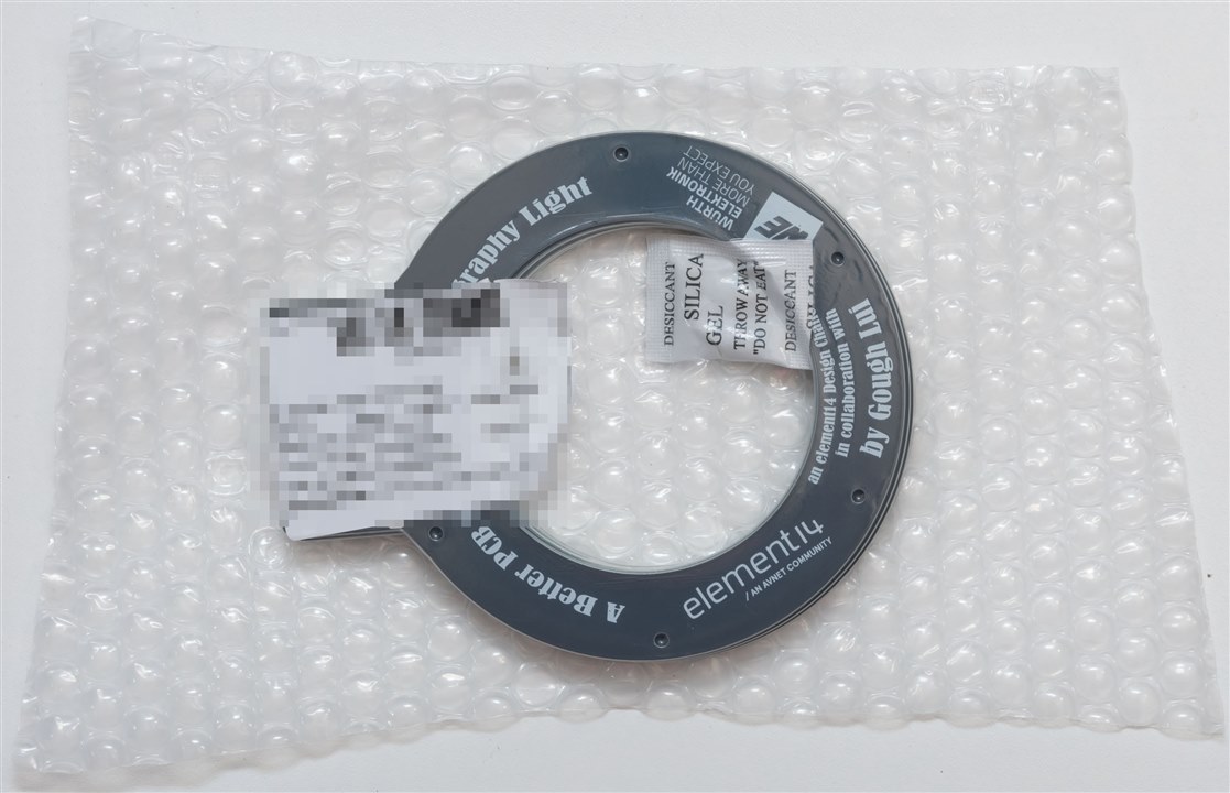
Just as designed, but made physical.
No Room for Mistakes!
This particular PCB poses a new challenge – a 5x5 array is 25 total LEDs. Well, our challenger kit only gives us 25 of that particular type of WL-ICLED, so there’s no room for mistakes. Don’t get nervous now! Getting nervous is a sure-fire way to make a mistake!
Let’s go about it in the same way – tin the pads.
Place and reflow the heat-tolerant components using top side heating and flux pen.
Wash off the flux to make it clean.
Apply fresh flux, place sensitive components, heat from underside. Then fit the other sensitive through-hole headers, using the Arduino Zero to guide the location of the header pins and hand solder.
Wash the board thoroughly and dry. Job done!
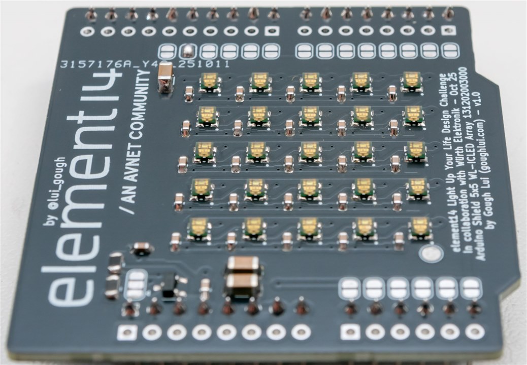
Perhaps a little too much solder as the joints are a hair on the blobby side.
No harm to the underside, even though I heated from the rear to get all those LEDs to solder. That’s just how I like it!
Testing the Boards
I modified the demoreel_100 demo as before, but with the correct settings for these LEDs and by adding a sequence that displays black, red, green, blue, white, black prior to the demo reel for testing. Rather than provide the whole program (as they are trivial changes), I’ll provide just the LED settings used –
Microscope Light Board
// FIRST STRING - EDGE FIRING
#define DATA_PIN    11 // Raspberry Pi Pico W
#define LED_TYPE    WS2812B
#define COLOR_ORDER GRB
#define NUM_LEDS    18

// SECOND STRING  - DOWN FIRING
#define DATA_PIN2    10 // Raspberry Pi Pico W
#define LED_TYPE2    WS2816
#define COLOR_ORDER2 RGB
#define NUM_LEDS2    18

// THIRD STRING – WIDE AREA DIFFUSE
#define DATA_PIN3    3 // Raspberry Pi Pico W
#define CLK_PIN3   2
#define LED_TYPE3    APA102
#define COLOR_ORDER3 GBR
#define NUM_LEDS3    18
Arduino Zero Shield
#define DATA_PIN    12 // Arduino Zero
#define LED_TYPE    WS2812B
#define COLOR_ORDER GRB
#define NUM_LEDS    25
As proof of functionality, I filmed a video of the boards running the tests with some commentary about the journey so far:
In all, the boards worked, but the WS2816 high-definition compatible “48-bit” type LEDs exhibited some sort of flicker when dimming up and down with FastLED compared to the 24-bit types. I suspect this may be due to the way that the extra bits are used, but it’s not a big issue as for me, the LEDs will mostly be “static” at various fixed settings. But for artistic applications, perhaps some investigation as to why the flicker occurs will be necessary.
3D Prints Completed and Revised
The first thing to be printed on my ailing Anycubic Mega P was the protection ring and the lens connection ring. To do this required a bit of tinkering with the Bowden tube which had torn off from the extruder and cleaning of the textured glass bed as it would seem that accumulated oils had resulted in poor bed adhesion.
For these parts, I chose to use a more premium PLA of a dark colour to avoid stray light reflections. For this, I ended up using my sample reel of Polymaker PolyLite Metallic PLA Pro in metallic blue.
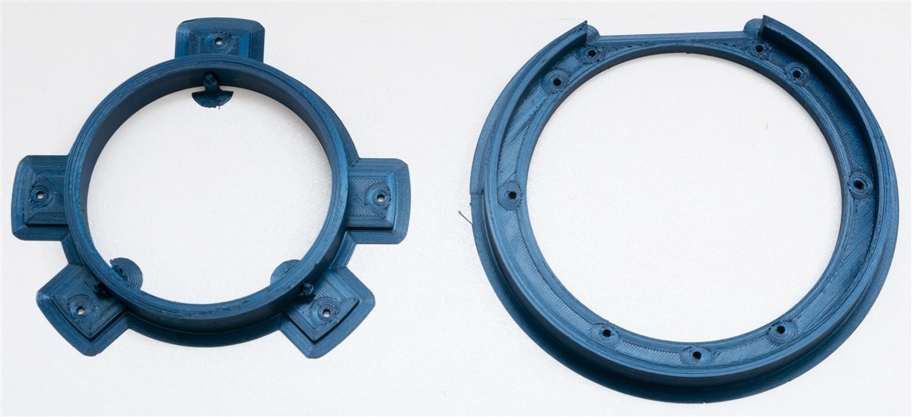
The prints were made with a skirt for adhesion, to avoid any issues with warping on the base. After removing the support, it was possible to assemble these parts together.
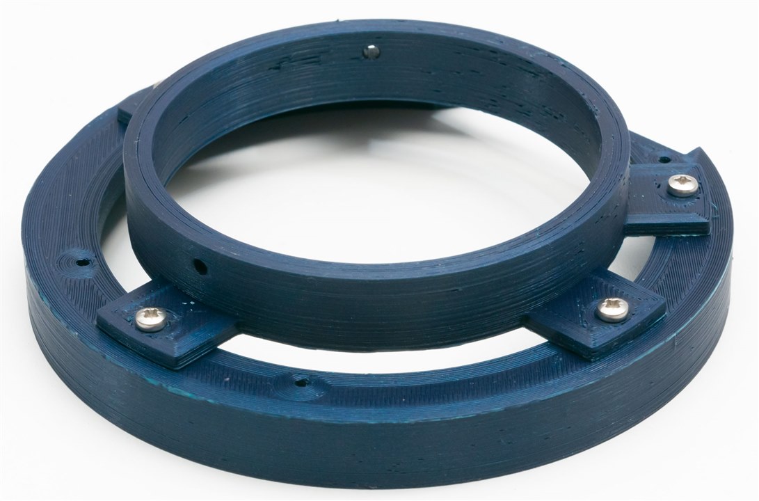
I used some short M3 screws to secure the two halves together for a solid connection.
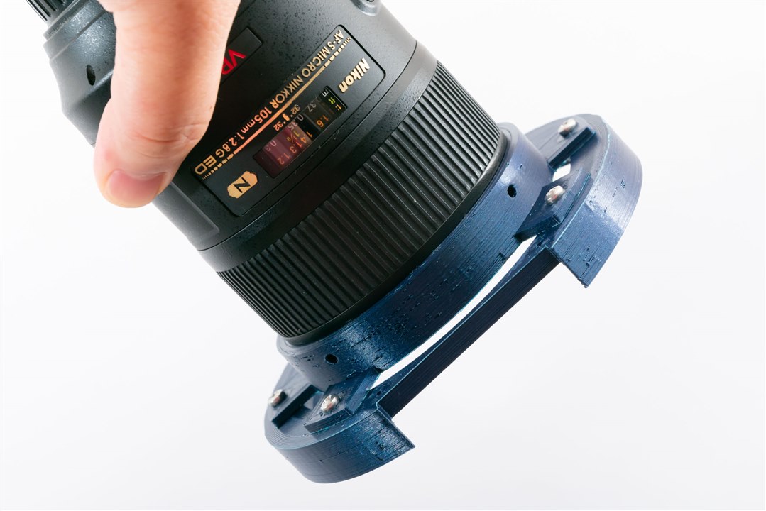
The diameter of the neck is just perfect to slip over the front of my NIKKOR 105mm macro lens and stay in place, just with friction. It is gripping on the coloured “gold ring” on the lens – a part that doesn’t rotate and does not interfere with the focusing ring or the filter threads.
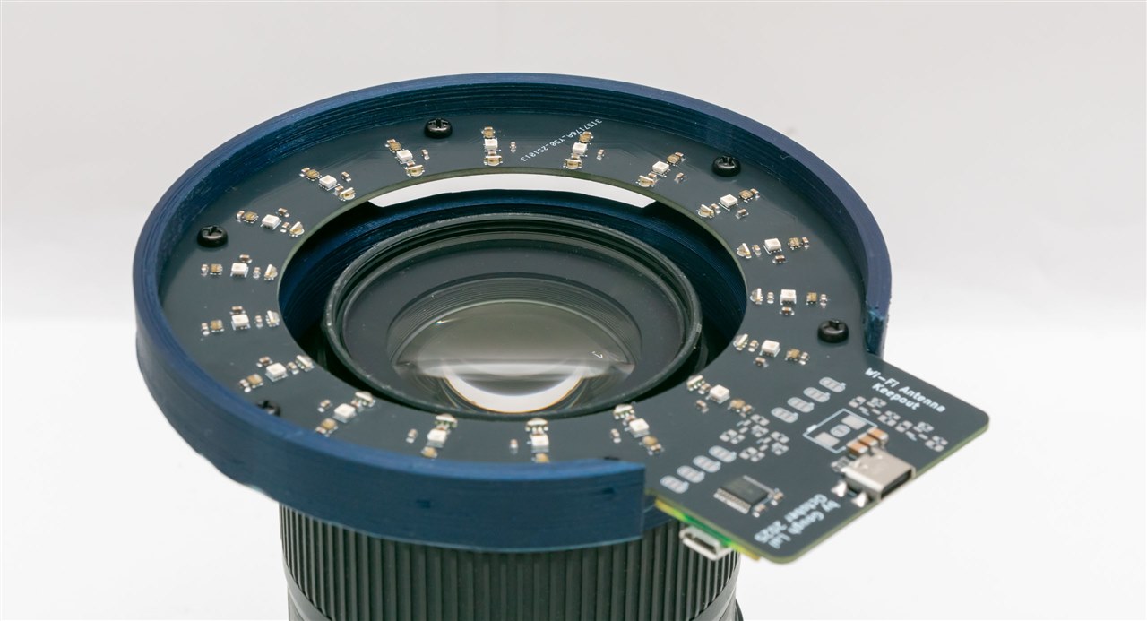
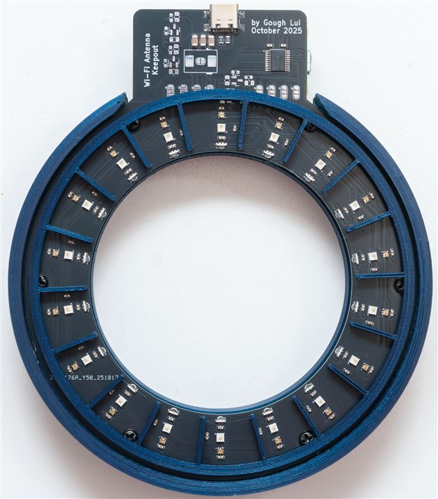
The board was installed into the assembly, with black M3 screws to avoid light reflections. It fit well for the most part, but the “handle” that has the Raspberry Pi Pico W didn’t quite have enough clearance, so I had to use side cutters to cut away some of the plastic to allow the board to sit properly. Because it was a minor bit of cutting, I decided it wasn’t necessary to revise the design.
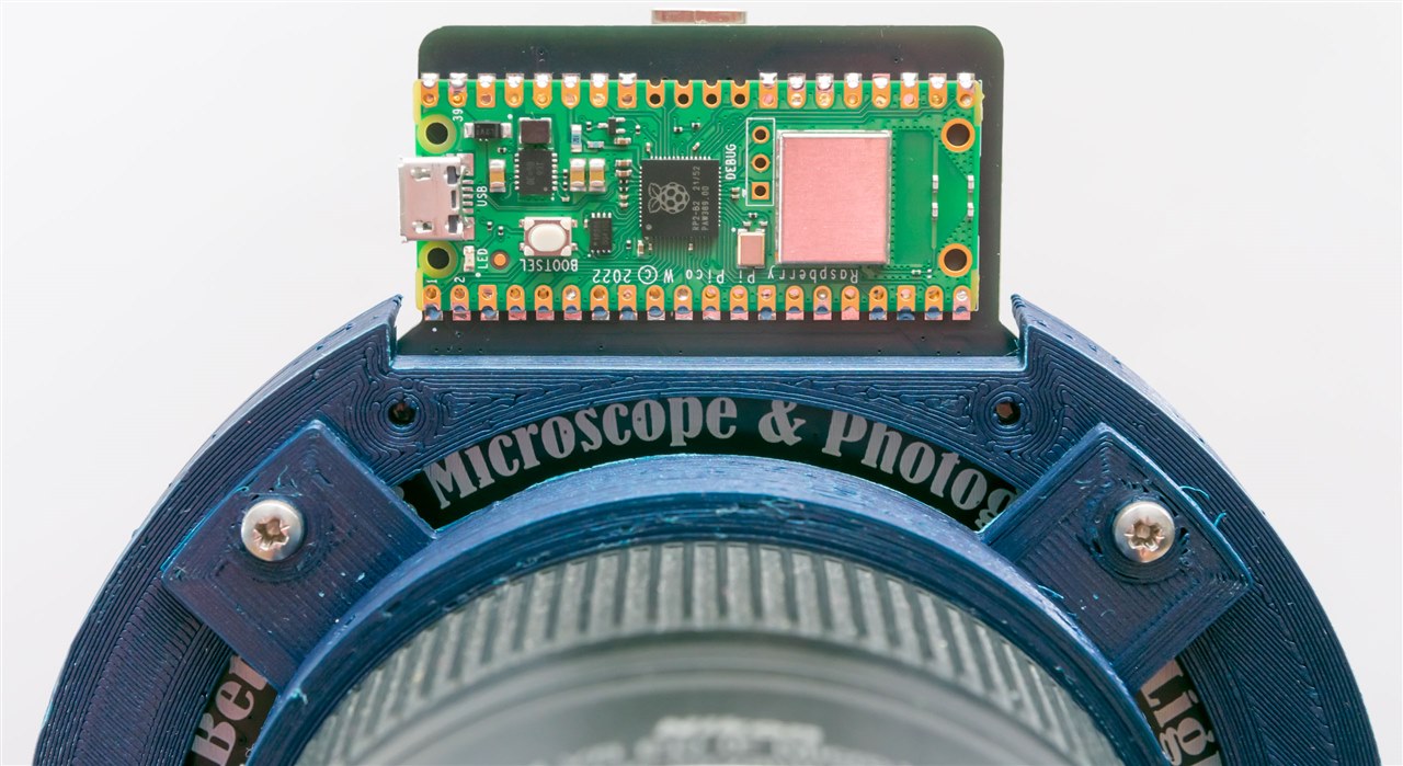
The design has a nice clearance around the Raspberry Pi Pico W. While it’s quite exposed, it’s also quite nicely “featured”. Too bad the silkscreen on the back is mostly covered.
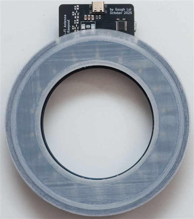
Ultimately, I thought the diffuser is absolutely necessary because some of the LEDs don’t “mix” the light quite well enough for my liking. So I decided to print a diffuser using some cheaper Kingroon Translucent PLA.
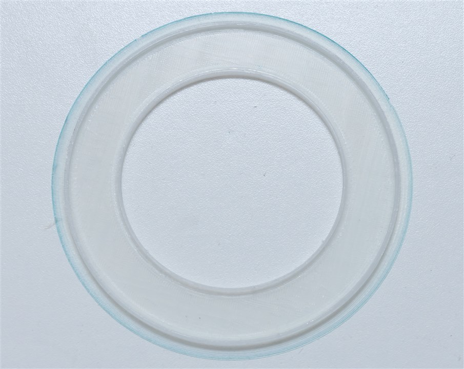
The original design was a tad too small for a friction fit, so I decided to make it a bit larger and deeper to make use of the “ribbed” texture of the prints to hold the diffuser in place automatically without the need of any fixing devices.
The result looks quite okay even without removing the skirt on the print.
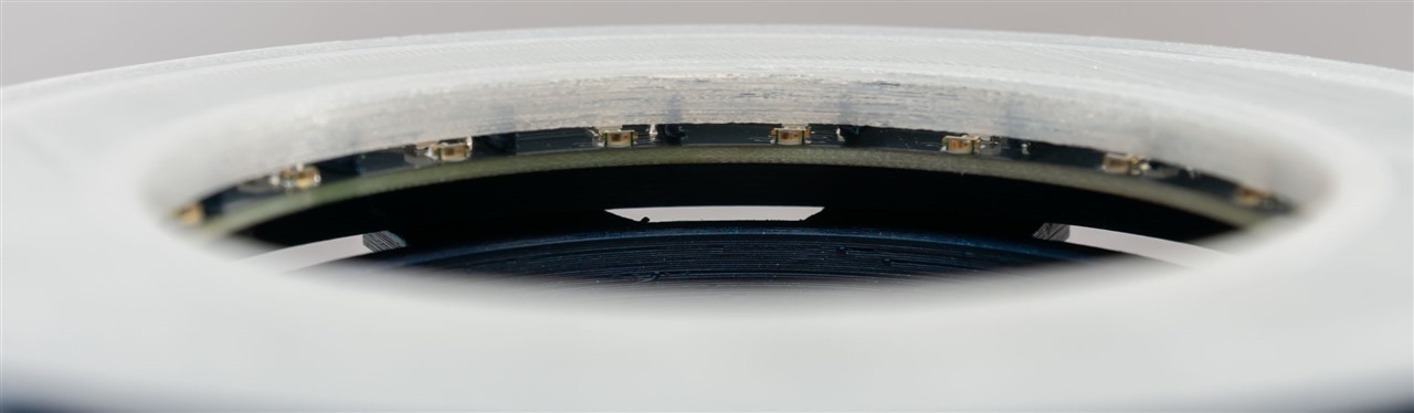
Because the 3D printed layers are at right angles, there is some enhanced diffusion effects. But the angular resolution didn’t seem quite on the level I had hoped as adjacent LEDs sort of “blended” into one another.
As a result, I had to go back to the drawing board …
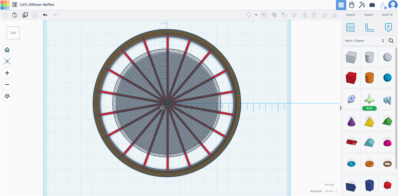
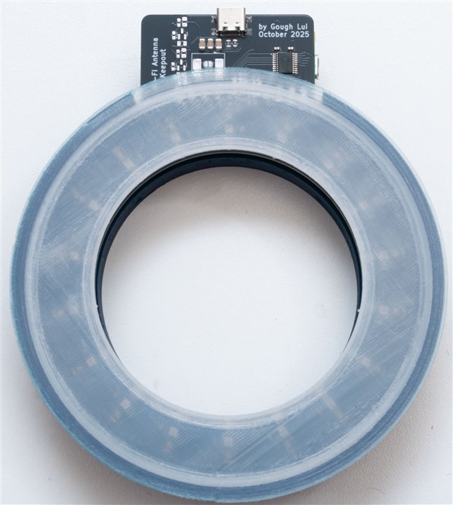
… and developed a baffle that could be inserted behind the diffuser. It would be slightly “big” – pushing from the inside of the diffuser while the outside ring is also pushing in from the outside, making it a nice “sandwich”.
The design needed a bit of fine tweaks to allow for the screw heads to not interfere too much.
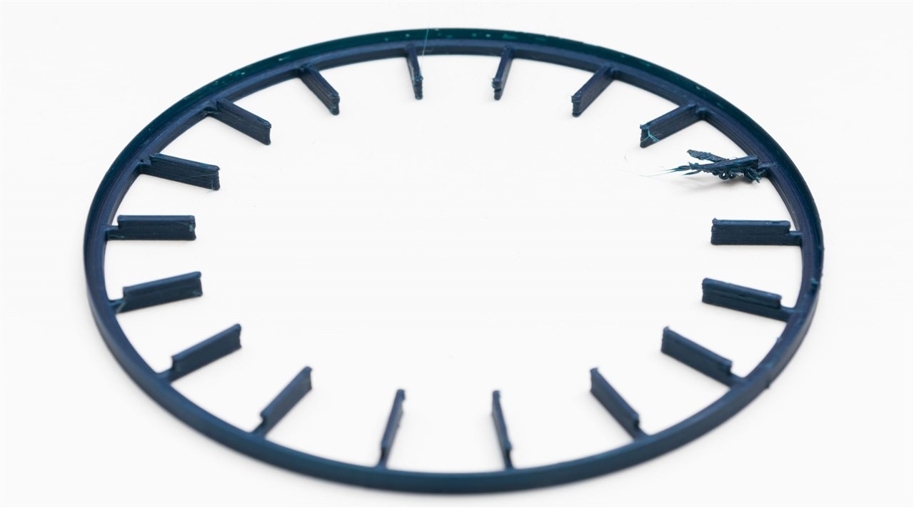
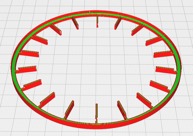
My first print wasn’t quite successful because of a loss of bed adhesion on one of the “fins”. But I decided to clean the bed and try again, which was successful. A print without skirts was chosen, as cutting away the skirts would have taken a lot of extra work.
While this isn’t 100% ideal for alignment, it was a design that would work – just being slightly off-set in terms of angle.
The sandwich with the baffle and diffuser in place …
… it doesn’t affect the clear gap for the edge-lit LEDs.
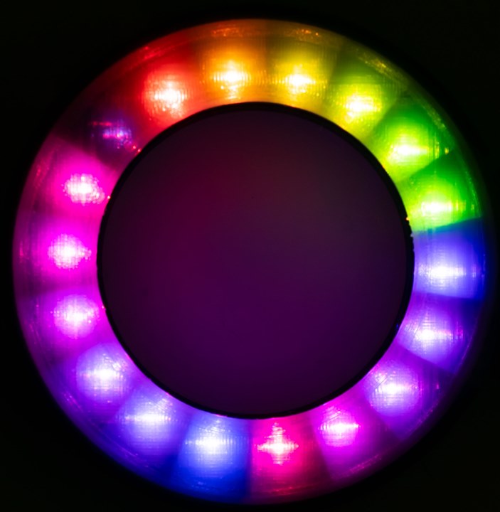
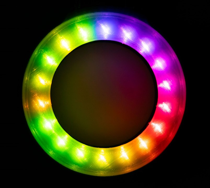
The light is much more compartmentalised now!
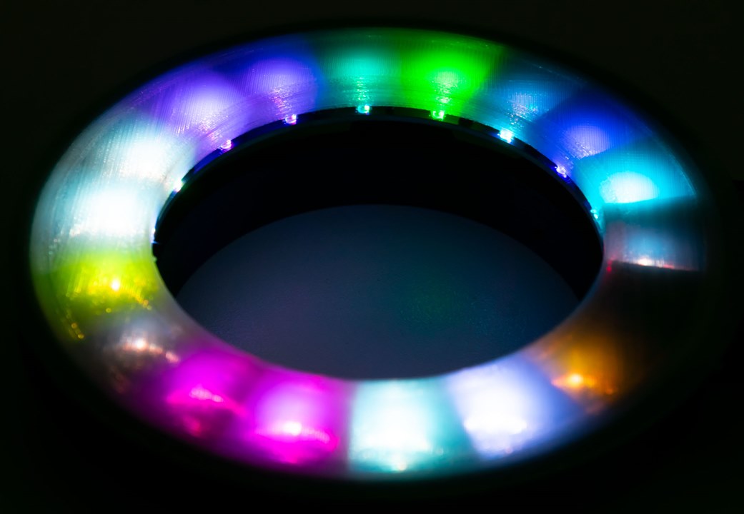
It almost reminds me of the “Wheel of Fortune” game show … but I feel this is much better than my first attempt!
If you’re interested, you can download the revised and additional STL files for 3D printing here:
LUYL-Gough-Lui-3DPrinting-New.zip
Conclusion
Now that all the hardware’s pretty much sorted and the challenge of design and construction have been overcome, the next frontier is the firmware or software aspects of the device. This will be an interesting challenge which will probably be the subject of the next posting. With the extension in contest time, it should be enough for me to fumble my way towards a solution, hopefully.
Let me know what you think of the progress so far and whether you’ve attempted any soldering on a similar scale yourself.


