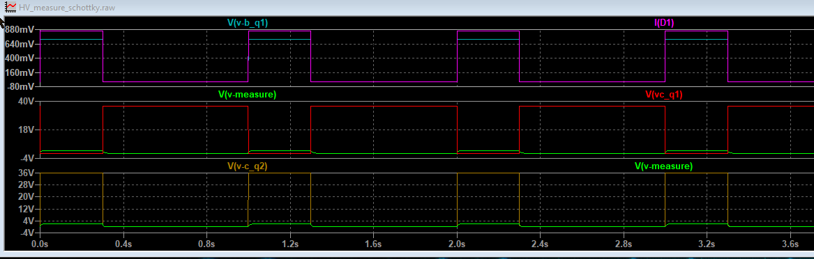
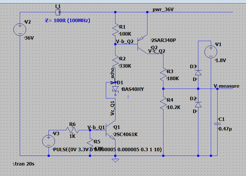
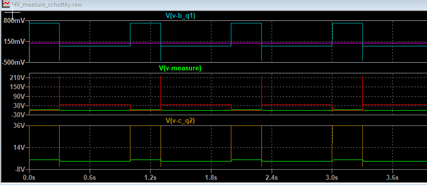
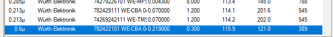
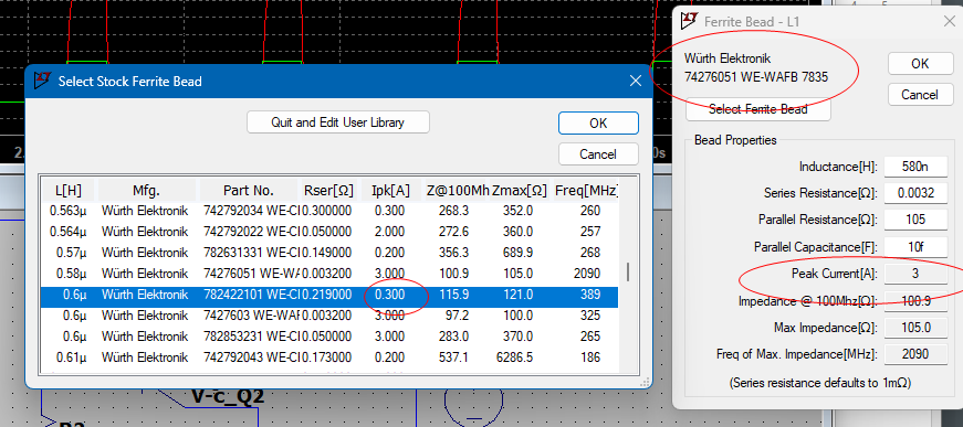
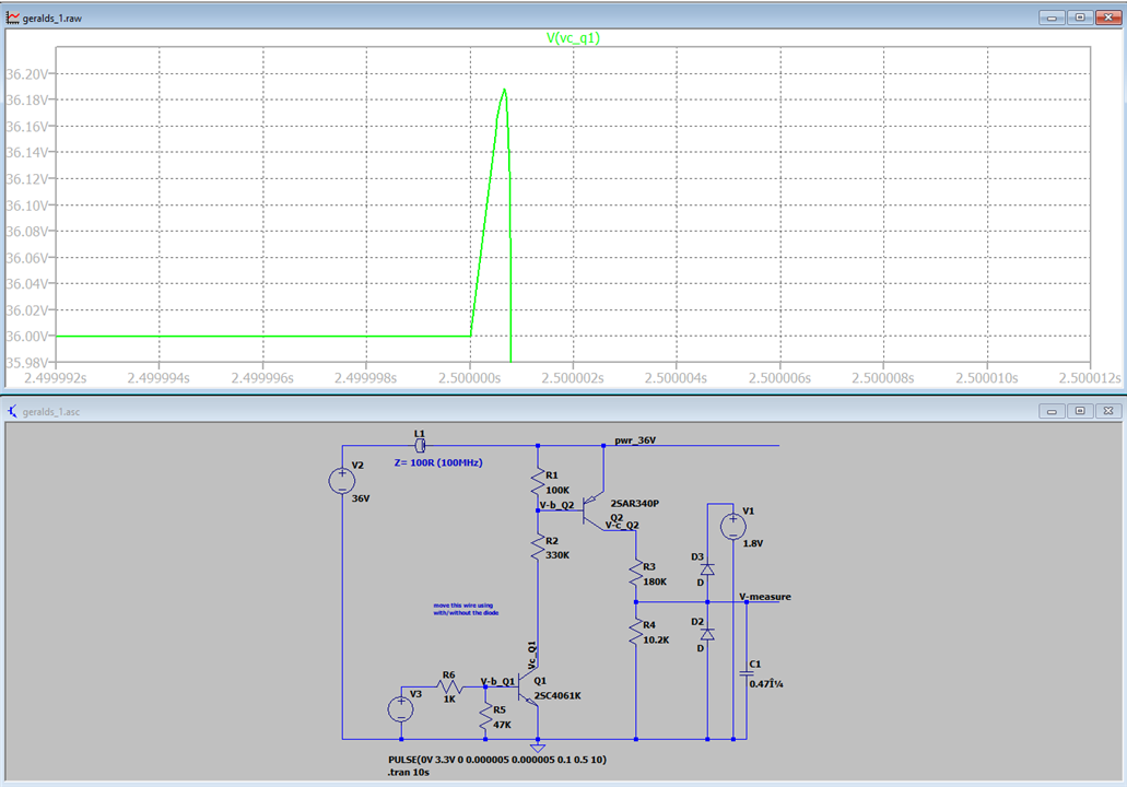
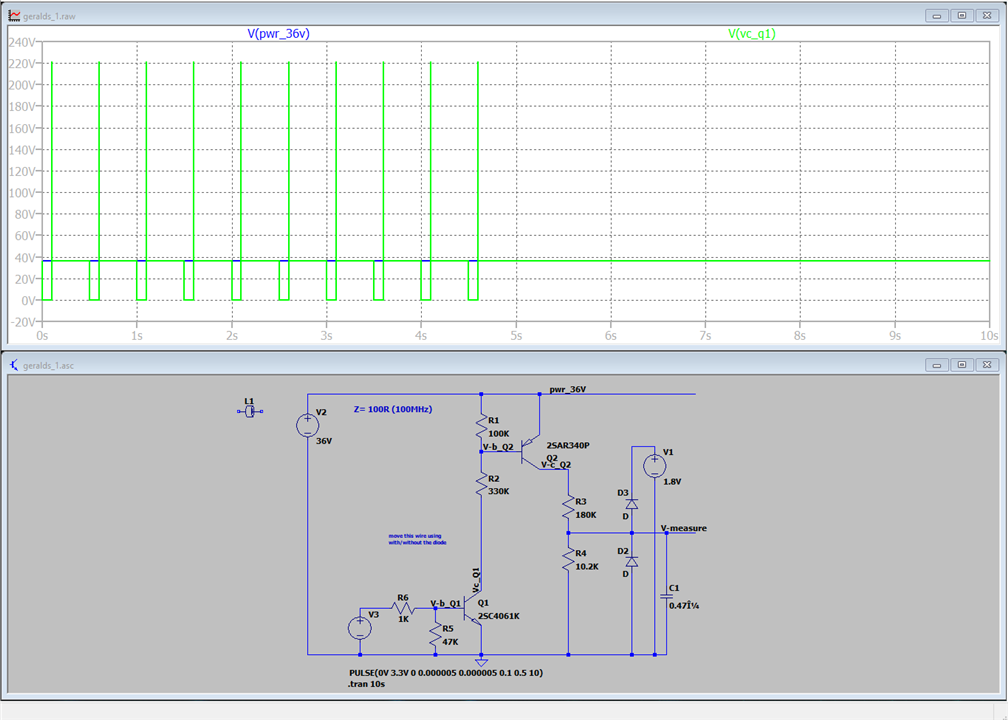
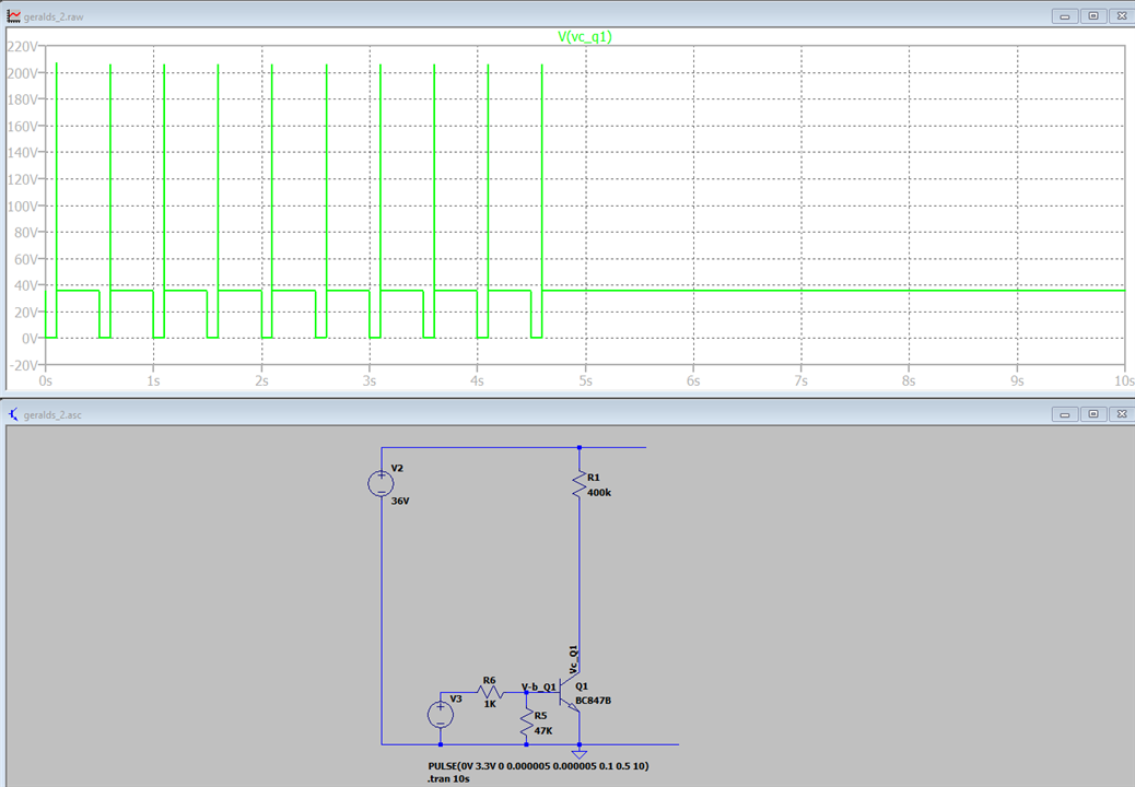
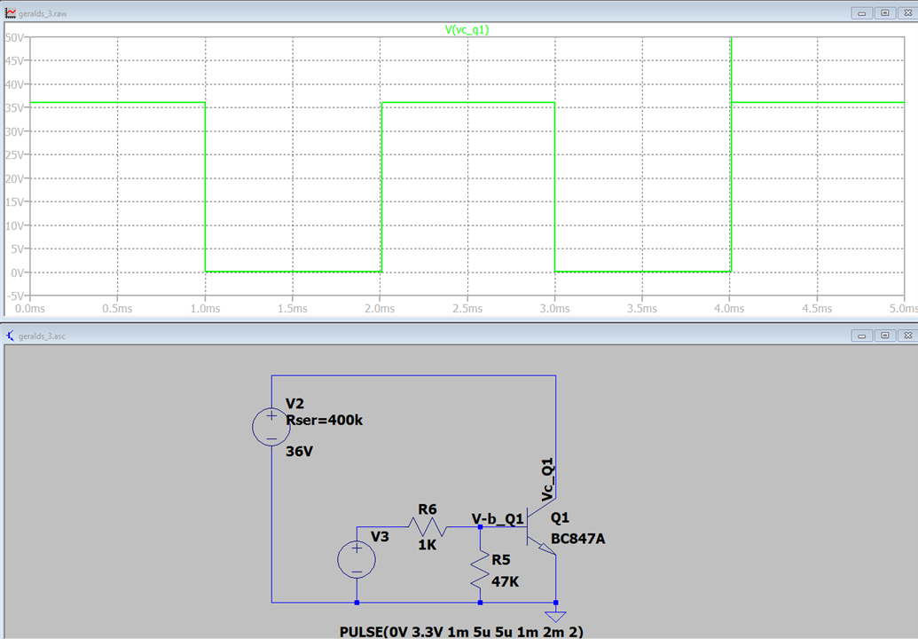
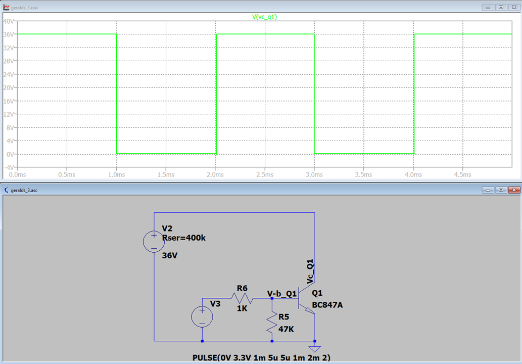
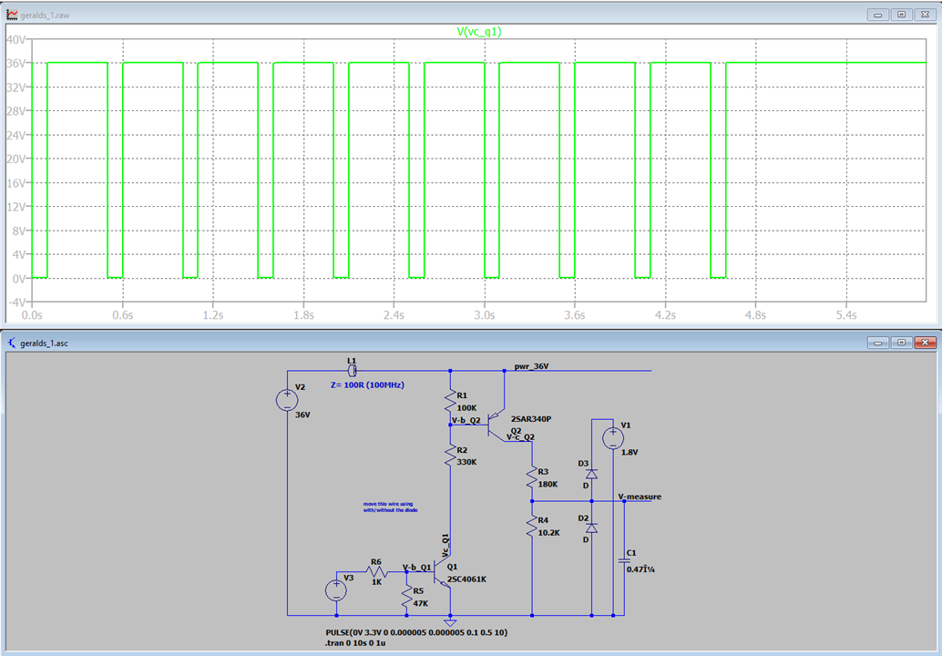
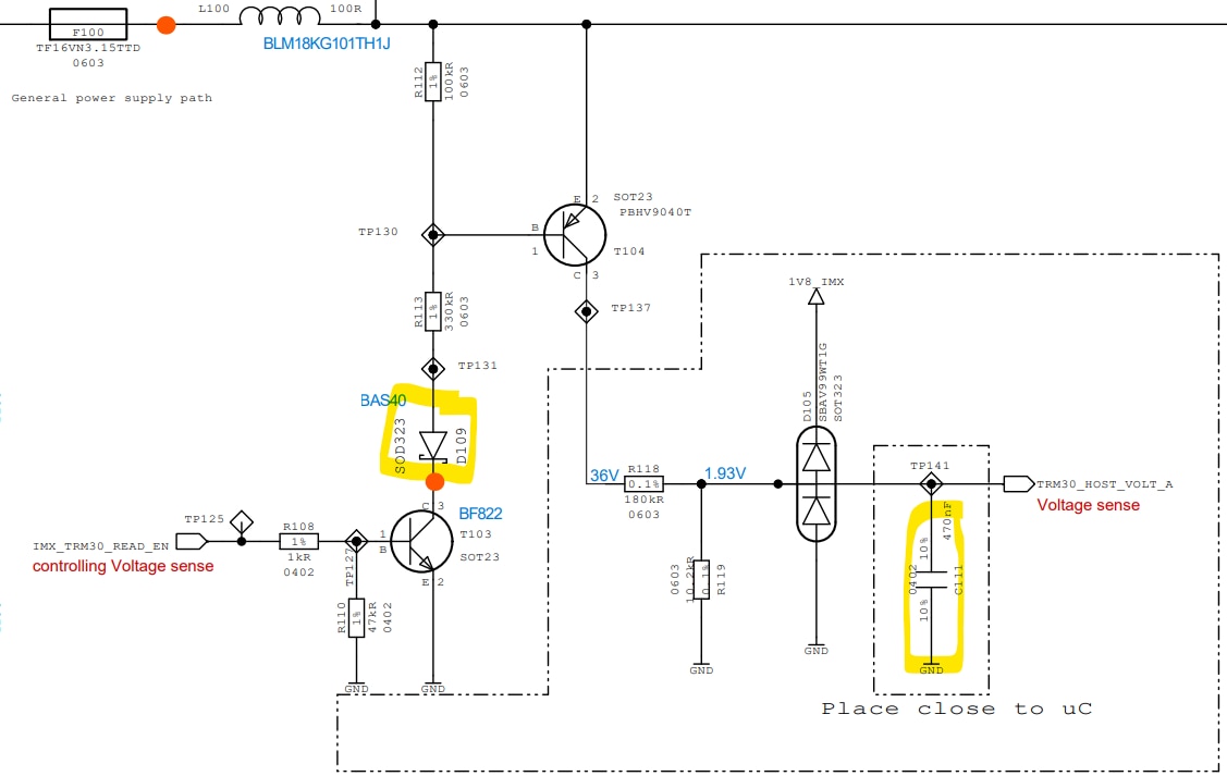
 Why is the Schottky diode being used in control circuit? and why is the 470nF cap is added at that voltage divider output? how is the Cap value 470nF calculated?
Be sure to click 'more' and select 'suggest as answer'!
If you're the thread creator, be sure to click 'more' then 'Verify as Answer'!
Why is the Schottky diode being used in control circuit? and why is the 470nF cap is added at that voltage divider output? how is the Cap value 470nF calculated?