


Continuation of Learning AMD Zynq: a project to generate a set of PWM signals. 1 - problem statement and possible approach .
yepe has a goal to create a set of signals for an ultrasone pulse generator.
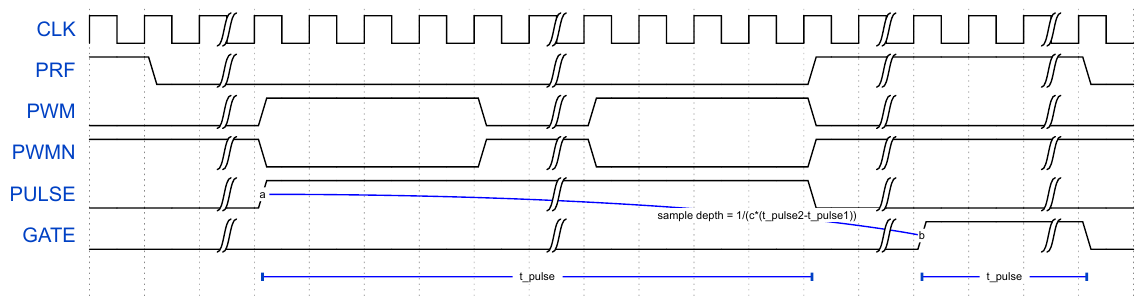
Status after Post 1
In Post 1, we got the PWM and PWMN signals, and a first stab at the PULSE signal. Let's start at that stable point here, and try to add
- the initial delay between PRF falling edge and the start of the pulse train
- a PULSE signal that starts and ends exactly when the pulse train starts and ends.
Here's the design from the 1st blog:
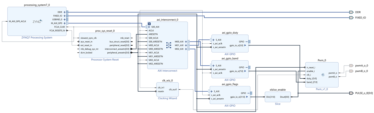
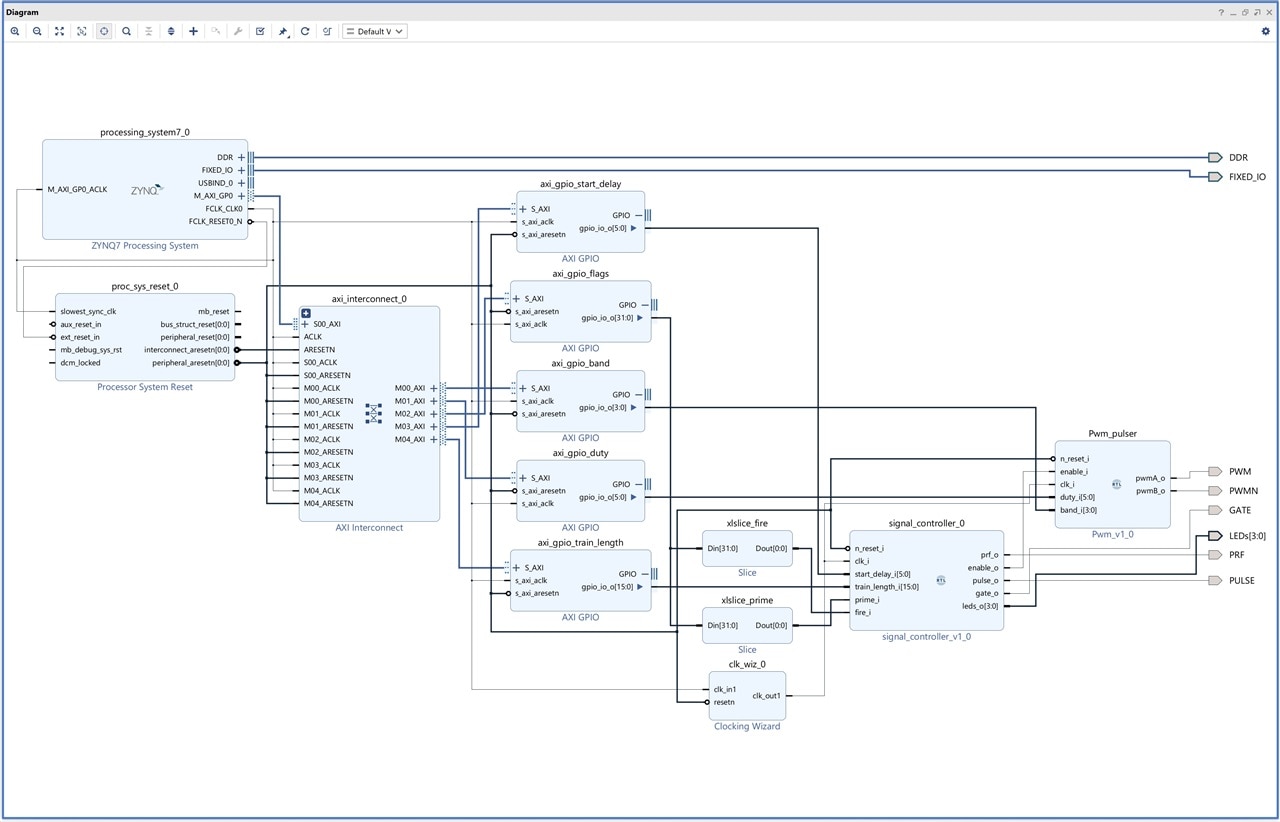
The clocking wizard generates a 320 MHz clock. High enough to give the PWM signal a decent granularity for the dead times (2.5 ns steps).
The PWM generator generates 2 complementary signals, PWM and PWMN, with configurable deadband.
The PWM generator has an enable pin. When that pin is low, it will set PWM low and PWMN high, else it outputs the train of pulses
Goal of this post:
- Build a control block that will tell the PWM when to generate pulses (control its enable)
- let that block also control the PULSE signal
- establish the configurable? delay at the start
- maybe handle PRF?
What this session will not do: handle GATE
Same as in post 1, the action will be in the comments. It's a collaborative exercise.
Update 4/5/2023:
Possible signal controller design (partly - not all states and signals implemented)
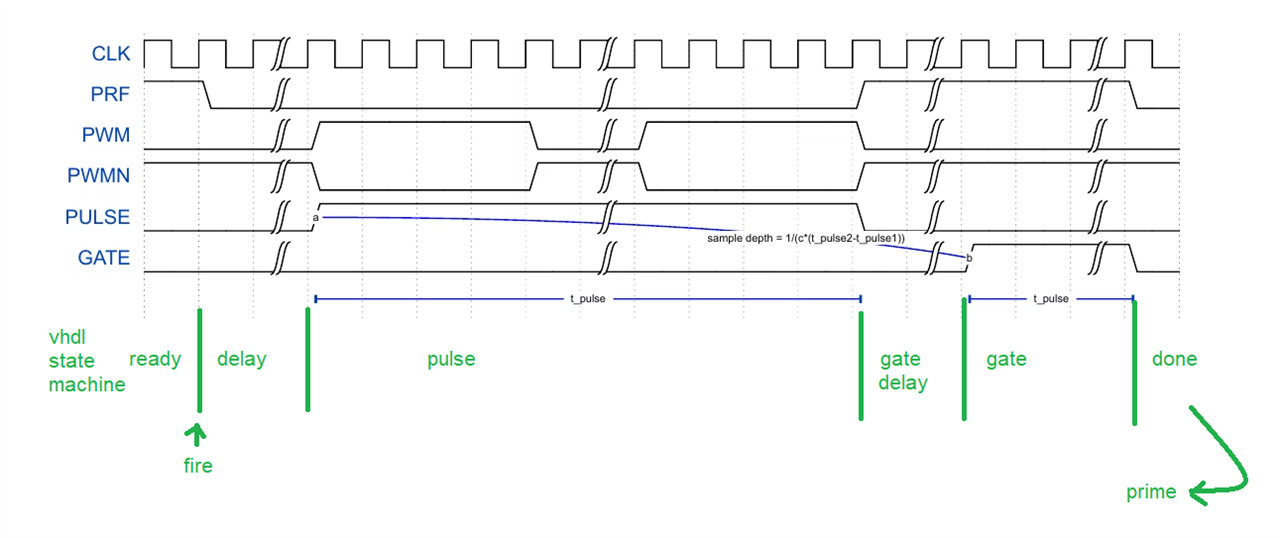
library IEEE;
use IEEE.STD_LOGIC_1164.ALL;

package PulsePckg is

    component signal_controller is
        generic (
            start_delay_resolution : integer := 6;  -- bit width of the counter used delaying pulse train start
            train_length           : integer := 7;  -- bit width of the PWM burst train counter
            gate_delay_resolution  : integer := 6;  -- bit width of the counter used delaying the gate signal start
            counter_resolution     : integer := 7   -- big enought o hold the largest of above
        );
        port (
            n_reset_i     : in   std_logic;                                                -- async reset
            clk_i         : in   std_logic;                                                -- Input clock.
            start_delay_i : in   std_logic_vector (start_delay_resolution - 1 downto 0);   -- Duty-cycle input.
            train_length_i: in   std_logic_vector (train_length - 1 downto 0);             -- how many PWMs in a burst train.
            prime_i       : in   std_logic;                                                -- allow cycle start
            fire_i        : in   std_logic;                                                -- start a cycle
            prf_o         : out  std_logic;                                                -- PRF
            enable_o      : out  std_logic;                                                -- enable pwm
            pulse_o       : out  std_logic;                                                -- PULSE
            gate_o        : out  std_logic;                                                -- GATE
            leds_o        : out std_logic_vector (3 downto 0)
        );
    end component;

end package;
library IEEE;
use IEEE.STD_LOGIC_1164.ALL;
use ieee.numeric_std.all;


entity signal_controller is
    generic (
        train_length           : integer := 7;  -- bit width of the PWM burst train counter
        start_delay_resolution : integer := 6;  -- bit width of the counter used delaying pulse train start
        gate_delay_resolution  : integer := 6;  -- bit width of the counter used delaying the gate signal start
        counter_resolution     : integer := 7   -- big enought o hold the largest of above
    );
    port (
        n_reset_i     : in   std_logic;                                                -- async reset
        clk_i         : in   std_logic;                                                -- Input clock.
        start_delay_i : in   std_logic_vector (start_delay_resolution - 1 downto 0);   -- Duty-cycle input.
        train_length_i: in   std_logic_vector (train_length - 1 downto 0);             -- how many PWMs in a burst train.
        prime_i       : in   std_logic;                                                -- allow cycle start
        fire_i        : in   std_logic;                                                -- start a cycle
        prf_o         : out  std_logic;                                                -- PRF
        enable_o      : out  std_logic;                                                -- enable pwm
        pulse_o       : out  std_logic;                                                -- PULSE
        gate_o        : out  std_logic;                                                -- GATE
        leds_o        : out std_logic_vector (3 downto 0)
    );
end signal_controller;

architecture arch of signal_controller is
    type states is (ready, delay, pulse, gate_delay, gate, done );
    signal counter : integer range 0 to 2**counter_resolution-1;
    signal state  : states;

begin


    clocked: process(clk_i)

    begin

        if rising_edge(clk_i) then
            -- sync reset
            if n_reset_i = '0' then
                counter <= 0;
                state <= ready;
                -- reset output states
                prf_o <= '1';
                enable_o <= '0';
                pulse_o <= '0';
                gate_o <= '0';
                leds_o <= (others => '0');
            else
                counter <= counter + 1;
                -- default output states
                prf_o <= '1';
                enable_o <= '0';
                pulse_o <= '0';
                gate_o <= '0';
                leds_o <= (others => '0');

                case State is

                    when ready =>  -- start a pulse group as soon as the fire bit is set
                        leds_o <= (0 => '1', others => '0');
                        -- check if the caller has reset the prime bit
                        if prime_i = '0' then
                            -- if yes, start if the fire bit is set.
                            if fire_i = '1' then
                                counter <= 0;
                                state <= delay;
                            end if;
                        end if;

                    when delay =>
                        leds_o <= (0 => '0', 1 => '1', others => '0');
                        prf_o <= '0';
                        if counter >= to_integer(unsigned(start_delay_i)) - 1 then
                            counter <= 0;
                            enable_o <= '1';
                            state <= pulse;
                        end if;

                    when pulse =>
                        leds_o <= (0 => '1', 1 => '1', others => '0');
                        enable_o <= '1';
                        prf_o <= '0';
                        if counter < to_integer(unsigned(train_length_i)) - 1 then  -- let the pulse change sync with last edge of PWM
                            pulse_o <= '1';
                        elsif counter = to_integer(unsigned(train_length_i)) - 1 then
                            pulse_o <= '1';
                            counter <= 0;
                            state <= gate_delay;
                        end if;

                    when gate_delay =>
                        leds_o <= (0 => '0', 1 => '0', 2 => '1', others => '0');
                        state <= gate;  -- todo implement

                    when gate =>
                        leds_o <= (0 => '1', 1 => '0', 2 => '1', others => '0');
                        state <= done;  -- todo implement

                    when done =>
                        leds_o <= (0 => '1', 1 => '1', 2 => '1', others => '0');
                        -- check if the caller has reset the fire bit
                        if fire_i = '0' then
                            -- if yes, prime if the prime_bit is set.
                            if prime_i = '1' then
                                counter <= 0;
                                state <= ready;
                            end if;
                        end if;

                end case;

            end if; -- sync reset
        end if; -- rising_edge

    end process clocked;

end architecture;
warning: the train length should always result in full PWM cycles. If you disable the PWM module before it had the chance to generate a full cycle, both PWM and PWMN will switch at the same time and not respect the deadband.
Block diagram:
Capture:
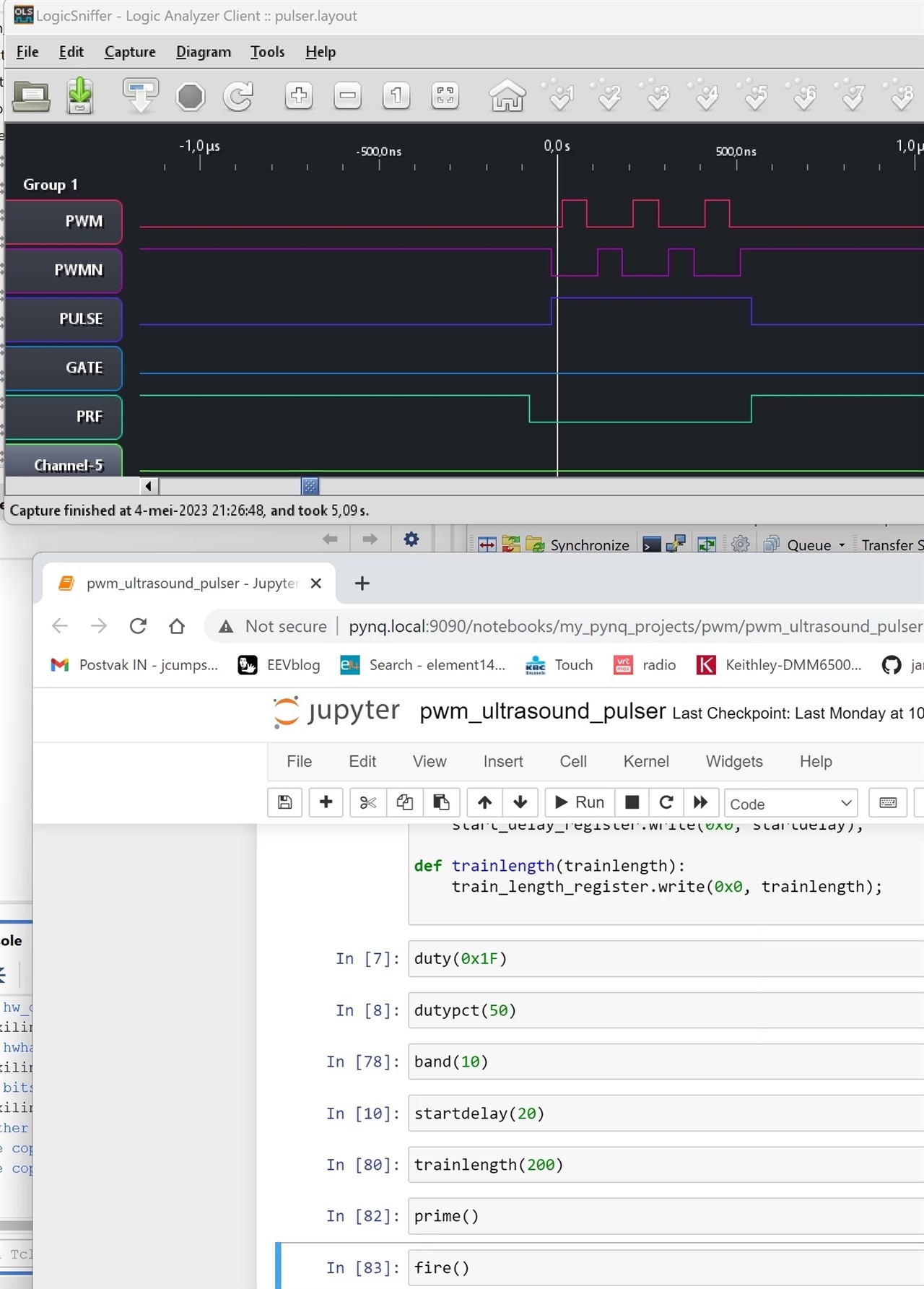
Jupyter:
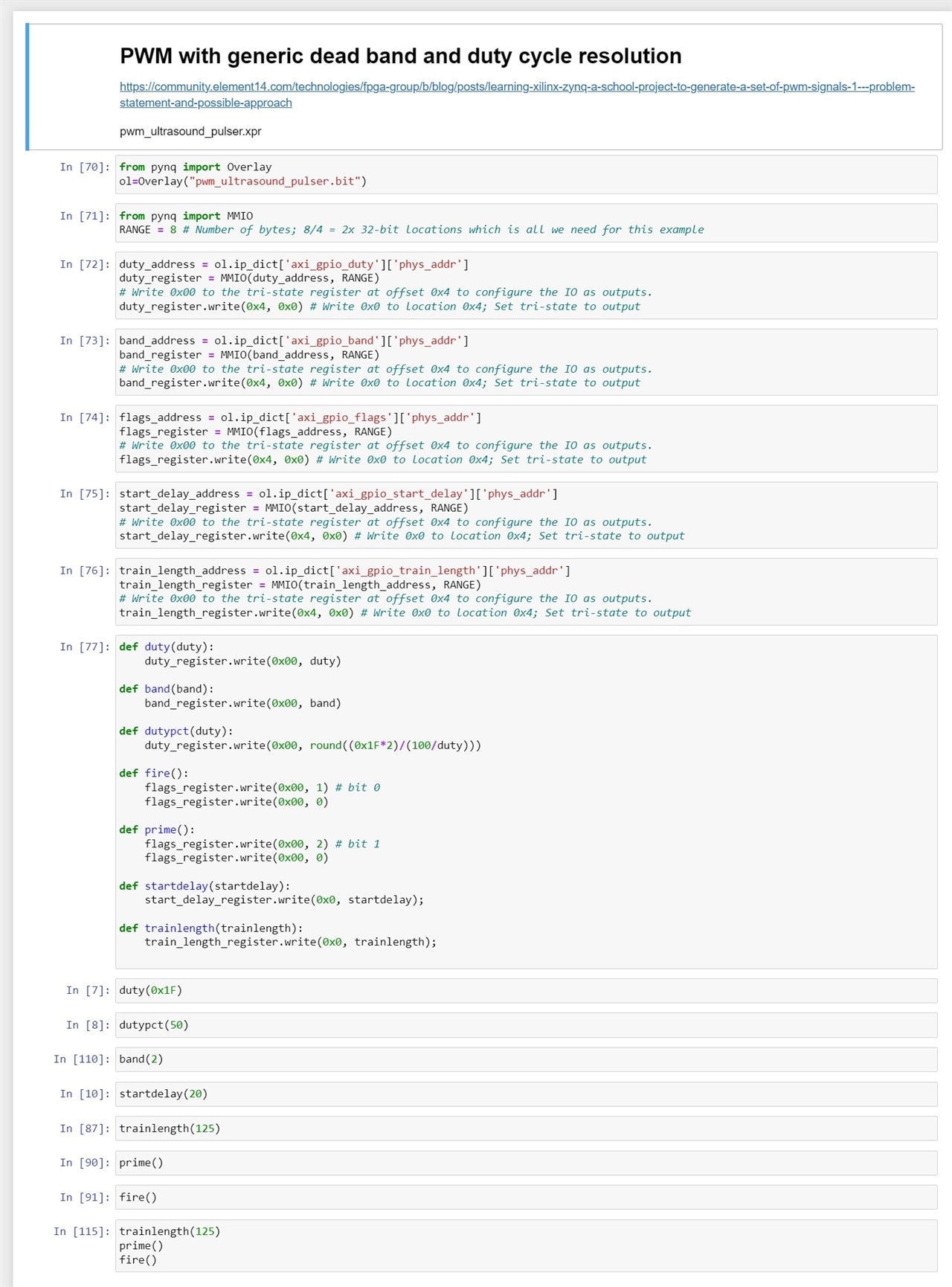
Jupyter source:
{
 "cells": [
  {
   "cell_type": "markdown",
   "metadata": {},
   "source": [
    "# PWM with generic dead band and duty cycle resolution\n",
    "\n",
    "https://community.element14.com/technologies/fpga-group/b/blog/posts/learning-xilinx-zynq-a-school-project-to-generate-a-set-of-pwm-signals-1---problem-statement-and-possible-approach\n",
    "\n",
    "pwm_ultrasound_pulser.xpr"
   ]
  },
  {
   "cell_type": "code",
   "execution_count": 70,
   "metadata": {},
   "outputs": [],
   "source": [
    "from pynq import Overlay\n",
    "ol=Overlay(\"pwm_ultrasound_pulser.bit\")"
   ]
  },
  {
   "cell_type": "code",
   "execution_count": 71,
   "metadata": {},
   "outputs": [],
   "source": [
    "from pynq import MMIO\n",
    "RANGE = 8 # Number of bytes; 8/4 = 2x 32-bit locations which is all we need for this example"
   ]
  },
  {
   "cell_type": "code",
   "execution_count": 72,
   "metadata": {},
   "outputs": [],
   "source": [
    "duty_address = ol.ip_dict['axi_gpio_duty']['phys_addr']\n",
    "duty_register = MMIO(duty_address, RANGE) \n",
    "# Write 0x00 to the tri-state register at offset 0x4 to configure the IO as outputs.\n",
    "duty_register.write(0x4, 0x0) # Write 0x0 to location 0x4; Set tri-state to output"
   ]
  },
  {
   "cell_type": "code",
   "execution_count": 73,
   "metadata": {},
   "outputs": [],
   "source": [
    "band_address = ol.ip_dict['axi_gpio_band']['phys_addr']\n",
    "band_register = MMIO(band_address, RANGE) \n",
    "# Write 0x00 to the tri-state register at offset 0x4 to configure the IO as outputs.\n",
    "band_register.write(0x4, 0x0) # Write 0x0 to location 0x4; Set tri-state to output"
   ]
  },
  {
   "cell_type": "code",
   "execution_count": 74,
   "metadata": {},
   "outputs": [],
   "source": [
    "flags_address = ol.ip_dict['axi_gpio_flags']['phys_addr']\n",
    "flags_register = MMIO(flags_address, RANGE) \n",
    "# Write 0x00 to the tri-state register at offset 0x4 to configure the IO as outputs.\n",
    "flags_register.write(0x4, 0x0) # Write 0x0 to location 0x4; Set tri-state to output"
   ]
  },
  {
   "cell_type": "code",
   "execution_count": 75,
   "metadata": {},
   "outputs": [],
   "source": [
    "start_delay_address = ol.ip_dict['axi_gpio_start_delay']['phys_addr']\n",
    "start_delay_register = MMIO(start_delay_address, RANGE) \n",
    "# Write 0x00 to the tri-state register at offset 0x4 to configure the IO as outputs.\n",
    "start_delay_register.write(0x4, 0x0) # Write 0x0 to location 0x4; Set tri-state to output"
   ]
  },
  {
   "cell_type": "code",
   "execution_count": 76,
   "metadata": {},
   "outputs": [],
   "source": [
    "train_length_address = ol.ip_dict['axi_gpio_train_length']['phys_addr']\n",
    "train_length_register = MMIO(train_length_address, RANGE) \n",
    "# Write 0x00 to the tri-state register at offset 0x4 to configure the IO as outputs.\n",
    "train_length_register.write(0x4, 0x0) # Write 0x0 to location 0x4; Set tri-state to output"
   ]
  },
  {
   "cell_type": "code",
   "execution_count": 77,
   "metadata": {},
   "outputs": [],
   "source": [
    "def duty(duty):\n",
    "    duty_register.write(0x00, duty)\n",
    "    \n",
    "def band(band):\n",
    "    band_register.write(0x00, band)\n",
    "    \n",
    "def dutypct(duty):\n",
    "    duty_register.write(0x00, round((0x1F*2)/(100/duty)))\n",
    "    \n",
    "def fire():\n",
    "    flags_register.write(0x00, 1) # bit 0\n",
    "    flags_register.write(0x00, 0)\n",
    "\n",
    "def prime():\n",
    "    flags_register.write(0x00, 2) # bit 1\n",
    "    flags_register.write(0x00, 0)\n",
    "    \n",
    "def startdelay(startdelay):\n",
    "    start_delay_register.write(0x0, startdelay);\n",
    "\n",
    "def trainlength(trainlength):\n",
    "    train_length_register.write(0x0, trainlength);\n"
   ]
  },
  {
   "cell_type": "code",
   "execution_count": 7,
   "metadata": {},
   "outputs": [],
   "source": [
    "duty(0x1F)"
   ]
  },
  {
   "cell_type": "code",
   "execution_count": 8,
   "metadata": {},
   "outputs": [],
   "source": [
    "dutypct(50)"
   ]
  },
  {
   "cell_type": "code",
   "execution_count": 110,
   "metadata": {},
   "outputs": [],
   "source": [
    "band(2)"
   ]
  },
  {
   "cell_type": "code",
   "execution_count": 10,
   "metadata": {},
   "outputs": [],
   "source": [
    "startdelay(20)"
   ]
  },
  {
   "cell_type": "code",
   "execution_count": 87,
   "metadata": {},
   "outputs": [],
   "source": [
    "trainlength(125)"
   ]
  },
  {
   "cell_type": "code",
   "execution_count": 90,
   "metadata": {},
   "outputs": [],
   "source": [
    "prime()"
   ]
  },
  {
   "cell_type": "code",
   "execution_count": 91,
   "metadata": {},
   "outputs": [],
   "source": [
    "fire()"
   ]
  },
  {
   "cell_type": "code",
   "execution_count": 115,
   "metadata": {},
   "outputs": [],
   "source": [
    "trainlength(125)\n",
    "prime()\n",
    "fire()"
   ]
  }
 ],
 "metadata": {
  "kernelspec": {
   "display_name": "Python 3 (ipykernel)",
   "language": "python",
   "name": "python3"
  },
  "language_info": {
   "codemirror_mode": {
    "name": "ipython",
    "version": 3
   },
   "file_extension": ".py",
   "mimetype": "text/x-python",
   "name": "python",
   "nbconvert_exporter": "python",
   "pygments_lexer": "ipython3",
   "version": "3.10.4"
  }
 },
 "nbformat": 4,
 "nbformat_minor": 2
}
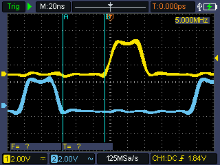
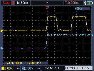
Scope capture (PWM, PWMN, PULSE, PRF)
0 dead time: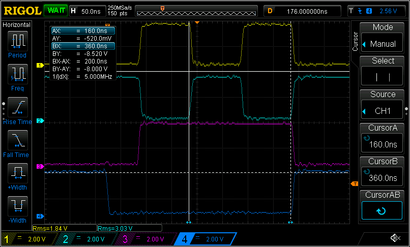
2 dead time: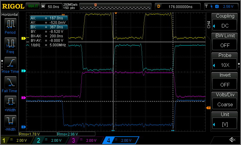
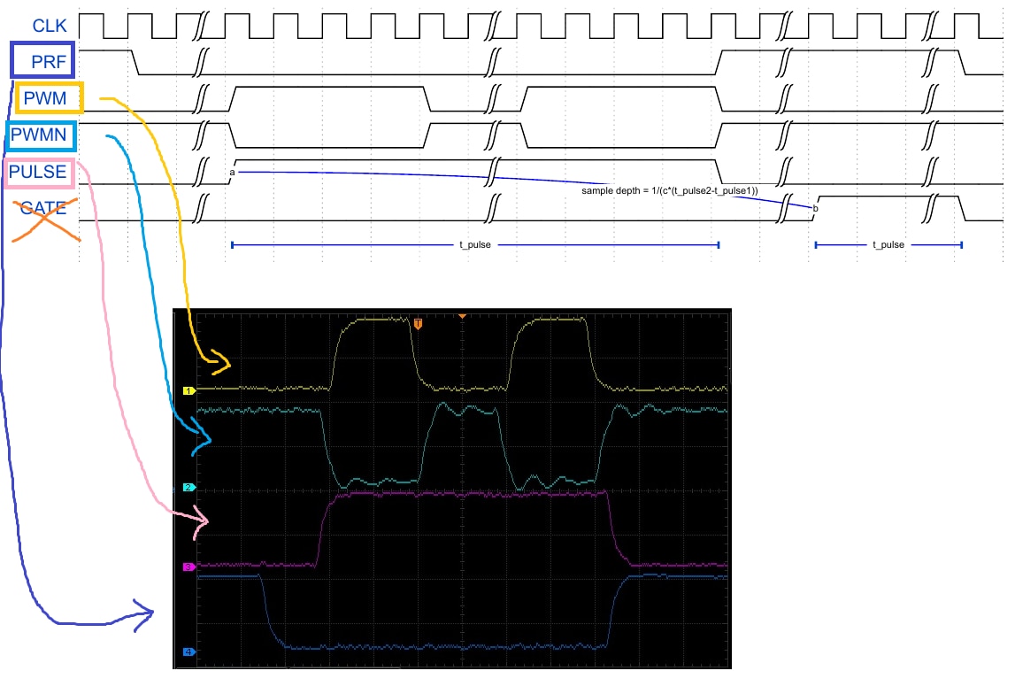
Compare to requirement:
Example with longer initial delay and a longer pulse train, 5 pulses of dead band. The FPGA design is the same. This is done by writing different values to the registers: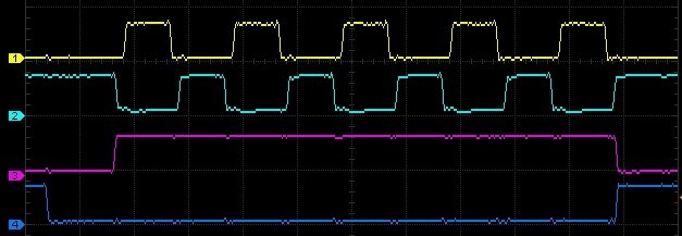
Study of the edges. You see the PWM and PULSE signal, 0 dead band.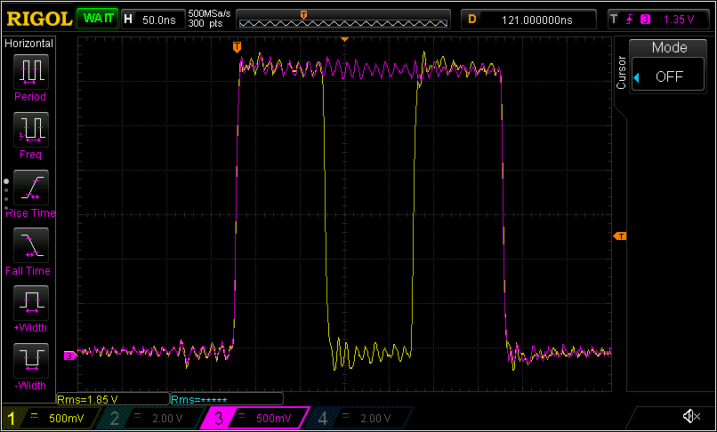
A few example settings that generate complete pulses. The first two generate 2 pulses, with a short start delay. The second 2 have a longer start delay and generate 5 pulses. The last one is retriggered in a software loop. I've also played with the deadbands.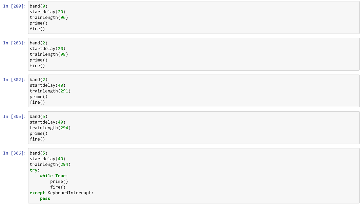
Vivado project and Jupyter notebook are attached. They are for version 2022.1 and PYNQ-Z2 board
pwm_ultrasound_pulser_and_jupyter_20230506.zip
Top Comments