My five optional blogs are in and it’s time to cap it off with a (mandatory) final blog, adhering to my “one blog a day” cadence to ensure I can deliver in time. As this blog needs to be standalone, it will be a slightly abridged summary of the points covered in all five optional blogs, with the results of a small last-minute push towards the finish line (see section Q9).
The intention for this series is to document my journey on learning about flyback transformers from the “ground-up” as someone with zero experience in implementing or using them. This post will be structured under a series of headings corresponding to questions that I had proposed answering as part of this Experimenting with Flyback Transformers Design Challenge. Backlinks to the optional blogs are provided for more detail where necessary.
Table of Contents
- Q1: What’s a Flyback?
- Q2: About the Bourns Flyback Transformers
- Q3: Performing Measurements of Key Characteristics
- Q4: What’s Inside a Flyback Transformer?
- Q5: What Happens to Flyback Transformers Under Abuse?
- Q6: Modifying an Existing Flyback Design
- Q7: Building a Very Basic Flyback Circuit to Step-Up
- Q8: What’s Missing from a Practical Design?
- Q9: The Final Push – Another Modification Attempt with a Boost Module Instead
- Conclusion
Q1: What’s a Flyback?
From hitting the books so to speak, there’s a few things to know. The first is that “flyback” as a term commonly refers to the flyback topology of power converter which utilises a flyback transformer at its heart.

Circuit schematic from Hudson, T., Ametller, M., How to Design a Flyback Converter in Seven Steps, n.d., Monolithic Power Systems (https://www.monolithicpower.com/how-to-design-a-flyback-converter-in-seven-steps).
The flyback topology itself resembles a buck-boost converter, with the inductor replaced by the flyback transformer instead (see Flyback Regulators here). The circuit can perform buck-boost functionality by virtue of the physics of turns ratio of transformers combined with the ability to adjust duty cycle and can produce multiple output voltages given different windings on the transformer (although usually only one output can be regulated). The transformer provides primary to secondary isolation, which is a positive for safety especially when working on mains voltage. The transformer itself also contains a gap, which increases the magnetic reluctance of the transformer, allowing for increased energy storage in the magnetic field by reducing the effects of core saturation. Therefore the transformer stores energy like an inductor, unlike ordinary transformers. The reason it is called a flyback is mainly because the voltage “flies back” as the switch opens, or so I’m led to believe. Such topologies are favoured for smaller converters as they are simple requiring no additional storage inductor, but really only suitable for power levels up to around 100-150W and currents up to 10A with a pulsating output. Output regulation generally requires either optocoupled feedback, a feedback winding or primary-side sensing. Some more resources are linked from Part 2.
Q2: About the Bourns Flyback Transformers
In February 2021, Bourns acquired Kaschke Components, a leader in providing customised magnetics and ferrite cores. While Kaschke is known for its custom capabilities, in May 2023, Bourns announced the release of “standard” products which are carried by distributors and ordered just like any other component. This has many potential benefits, especially for small quantity requirements, reduced lead times and broad availability, allowing more consumers to access Bourns (formerly Kaschke’s) expertise and quality.
The provided kit included one of twelve different types of components. But curiously not all products are flyback transformers.

I extracted all the product details into a summary table above. As it turns out, #1 and #2 are power-line communication transformers, which appear to be useful for coupling data signals into power lines. Items #4 to #10 are indeed flyback transformers, all from the SP-E range which incidentally stands for SmartPower Safety Transformer which appear mostly geared towards mains-voltage power supplies optimised for operating at 132kHz. Finally, item #11 and #12 are SP-E filter chokes which are commonly used in switching power supplies to suppress electromagnetic noise, with these units intended to be a good match for the flyback transformers. It would seem #3 is a bit of an odd-one-out, being a flyback transformer but a very small surface-mounted unit from a different series, intended for automotive AEC-Q200 qualified 7-24V usage.
The Bourns products are still marked with Kaschke markings in some cases and mostly feature red plastic ends. Some utilise yellow insulating tape over their windings, while some also use insulated wire for their windings as well. A much closer look at each is provided in Part 1.
Q3: Performing Measurements of Key Characteristics
With the components in hand, I thought it would be important to measure certain characteristics just to confirm datasheet values and identify differences between different types of transformers.
LCR Measurements
I decided to use the B&K Precision BA6010 Battery Analyser as an LCR meter. This meter is intended for use in measuring AC internal resistance for batteries and acts like an isolated 1kHz AC LCR meter. While its ranges and accuracy may not be as good as a proper benchtop LCR meter, it’s more accurate than most handheld meters.
To back this up, I decided to also use my Agilent (now Keysight) U1733C Handheld LCR Meter for higher frequency, 10kHz testing.
This should be a closer match to datasheet testing conditions, although I was not able to match the test current in all cases as the meter decides what current to use.
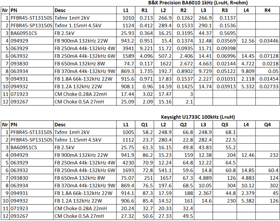
In general, the measured parameters match quite well with the datasheet specifications and measurements between equal windings only differed slightly, in part due to slight wire length and test lead positioning differences between tests.
Bode Plots and Waveforms
Another thing I thought was worth measuring was just how these transformers behave in the frequency domain and with square wave excitation at various frequencies, compared to ordinary mains transformers.
For this, I used a Rohde and Schwarz MXO4 Oscilloscope (review pending) with its onboard signal generator to run some bode plots on a few products.
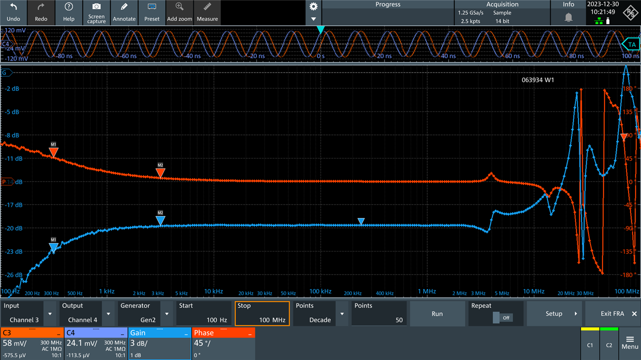
Looking at this test of a flyback transformer, it seems that the gain tails off in the low frequency end around 2kHz. I presume this is because of core saturation effects. Towards the 4MHz region, there is a bit of a dip, but self-resonance doesn’t seem to occur until 25MHz (or is that just my clip ground lead). Nevertheless, this reminds us that part of the “magic” of the small transformer is in its higher operating frequency than the mains transformer.
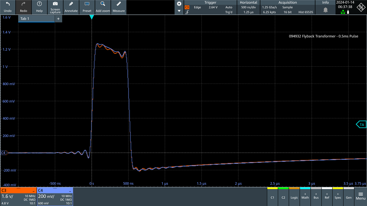
Driving a 0.5ms pulse into a flyback transformer results in faithful reproduction.
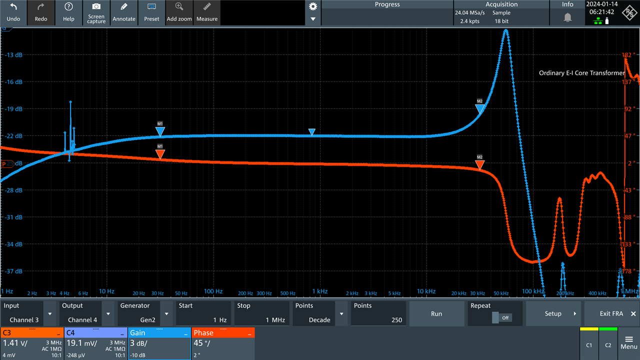
Taking the ordinary E-I core mains transformer, and ignoring the few gain spikes due to range switching, we can see that it is happier at low frequencies but starts deviating significantly by the time we pass 20kHz, being self-resonant before 100kHz.
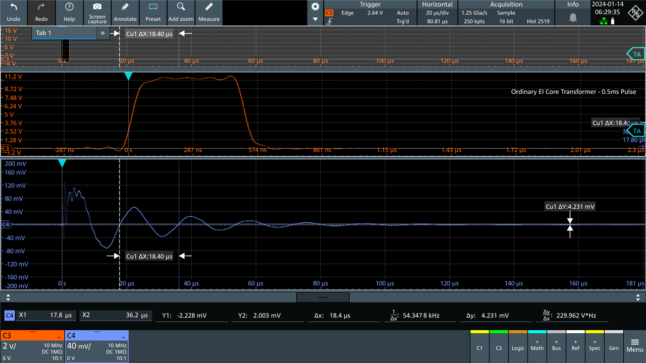
When this E-I transformer is excited by a 0.5ms pulse, it sort of “rings” around 54kHz.
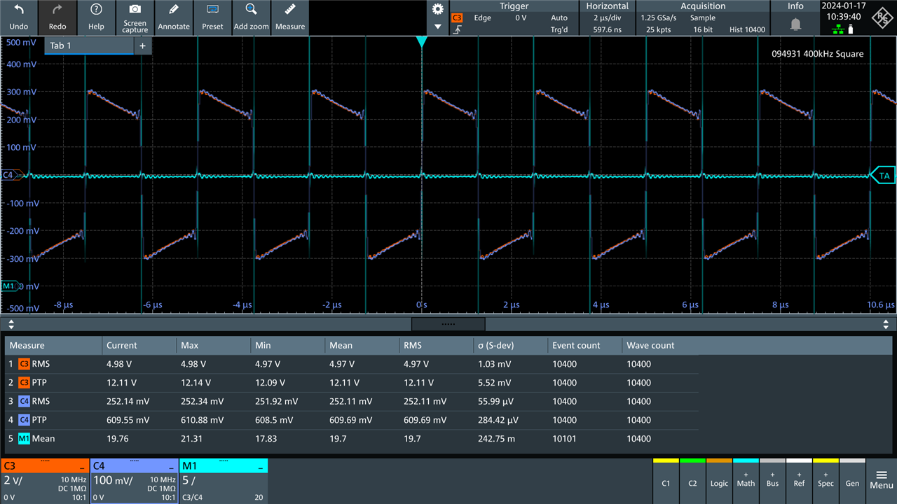
This common-mode choke could sort of be used like a 1:1 transformer. Unlike the flybacks, it seems happier down to low frequencies as well, starting at 100Hz it is flat!
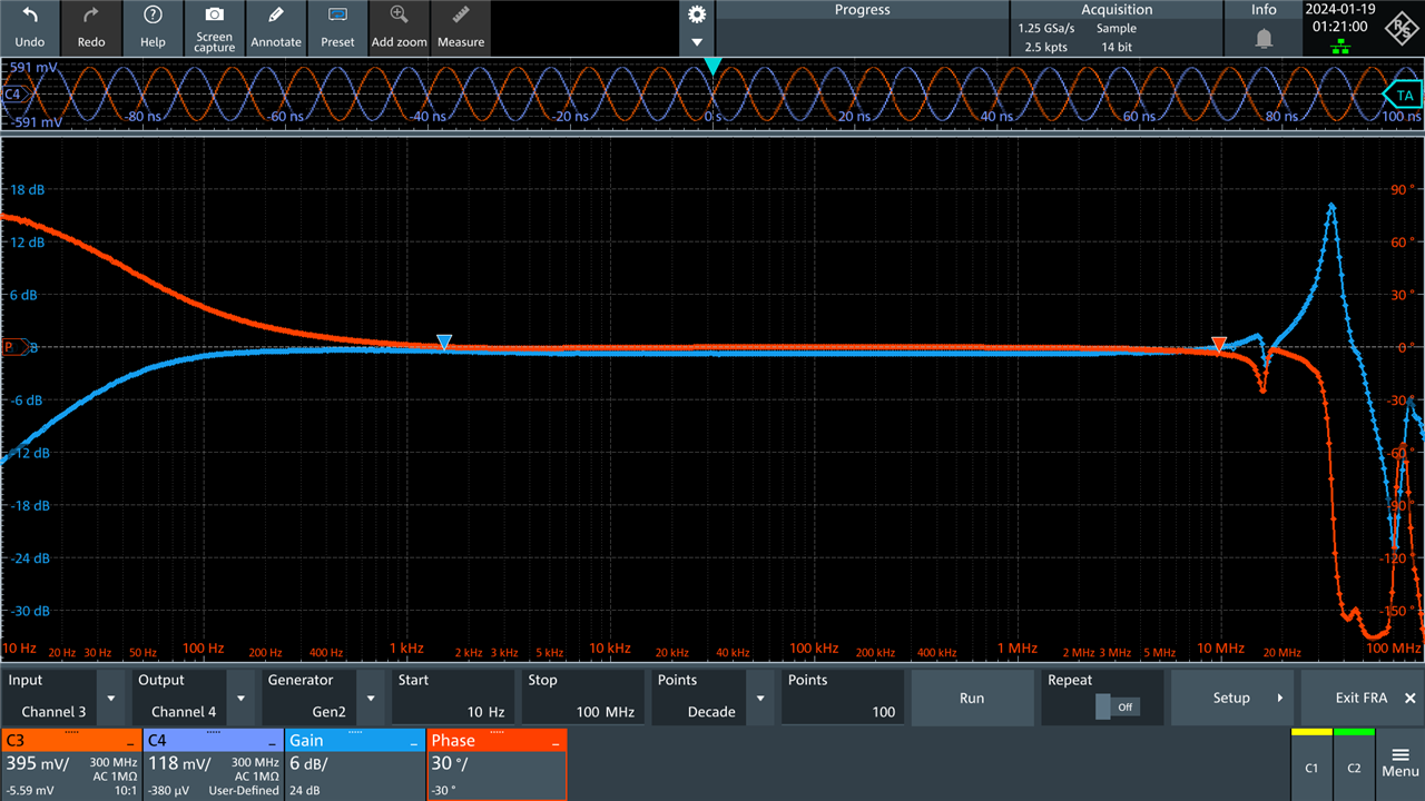
Testing of the ordinary PLC transformer (PFBR45-ST13150S) showed an excellent flat bandwidth response across a range of frequencies starting at around 45Hz (-3dB) and extending past 10MHz. Above there, the mess that is visible is likely due to the clip grounds. The reinforced insulation version had virtually identical results.
More results are contained in Part 2 and Part 4.
Insulation Resistance
The insulation on a flyback transformer is the reason why flyback converters are considered isolated. Having good insulation is vital to ensure there is no leakage of current or connection between the primary and secondary. This is especially important for the safety of the user as humans can come into contact with the output. Therefore, it is good to see that Bourns rates most of their transformers as having insulation with working voltages of 400V DC and a rated dielectric strength of 4.2kV @ 50Hz for 1-sec. Unfortunately, I don’t have a Hi-Pot tester, but I do have the Keysight U1461A Insulation Resistance Test Multimeter which I recently replaced the OLED display on. This unit is capable of up to 1000V DC test voltages.
It seems unsurprising that there were no problems with this test on all my transformers. The display simply reported >260GΩ after a short time charging up the capacitance in the test leads and transformer.
A couple more examples are shown in Part 3.
Q4: What’s Inside a Flyback Transformer?
This brings me to the question – what are the secrets of the Bourns flyback transformer? Where is this “magical” gap that I’ve heard all about and just how does the insulation work? Well, unfortunately for one flyback transformer (063929), it has been chosen as the sacrifice in the name of science.
To open up the transformer, one has to first break apart the ferrite core. The core itself appears to be made of two parts, glued together. The glue is very strong, so I wasn’t able to break it neatly. Instead, a heavy tap with a screwdriver shattered the ferrite in multiple places, which continued to break under prying. The centre section of ferrite was very snugly located in the bobbin, requiring some careful hammering to remove.
There we go – the plastic bobbin with the windings and the core are now separated. A closer look at the core seems to show that the gap is in the middle where it cannot be seen. Any gaps on the outside or misalignments are probably not the intentional gap. This centre gap, at least on this side, has some discolouration which might suggest some manufacturing process which may have created some heat or chemical process which may have affected the surface of the ferrite on this side.
Turning it over, the discolouration does not appear to be present although there seems to be more of the glue on this side. This suggests that the cores may not be quite perfectly shaped or aligned during manufacture.
The secondaries are parallel wound in a pair using insulated wire that has yellow insulation. I’m not sure what the jacketing material is made out of.
The secondary is isolated from the shield (if present) and primary by this plastic film layer. The design of this insulator is quite good, as it is wrapped around in a few layers, is longer than just the winding part of the bobbin, having slitted sections on the outside to provide additional insulation “skirt” that makes it difficult for any tracking to occur.
The adhesive was quite strong, so removing the insulation took some care with tweezers.
The primary is wound using thin enamelled copper wire. The primary appears to be wound in two layers and is the closest to the core.
Q5: What Happens to Flyback Transformers Under Abuse?
Mains transformers frequently have thermal fuses embedded in their primary windings just in case something goes wrong and the transformer ends up overheating, but I didn’t see anything like that in the flyback transformer. The primary winding in the previous transformer was also very fine, not unexpected for the low power rating, but does this mean there’s a chance that the winding itself will burn open like a fuse, or will it all heat-up and catch fire if the switching transistor blows through and the coil just ends up being shorted over a supply.
For this experiment, another flyback transformer (063932) was sacrificed in the name of science. As I didn’t want to risk any major damage, I restricted myself to 12V/2A from a Keysight E36103A into the primary which is intended for mains 85-265V AC applications. This would limit dissipated power to 24W at the most, which would limit the chance of harm in this test. The test was observed with my Nikon D3400 DSLR and a Infiray P2 Pro Thermal Camera.
The results were interesting. When power was applied, I expected the transformer to saturate quickly and for it to act like a short over the supply, dragging its voltage down to near zero. Instead, it seemed that the transformer’s reluctance was enough to keep it at 12V/2A for quite a moment until it heated up enough to cause internal damage. During this sequence, the secondary windings started to move slightly and change colour as its insulation was exposed to the heat. Some smoke began to issue from the transformer with a few popping sounds and the temperature peaked at around 188°C. Afterward, the voltage from the supply began to drop, likely as the primary coil started to short out and the temperature began to drop. The coil did not go open circuit and the reduced power dissipation resulted in the transformer staying in the ~120°C range. After a couple of minutes, I turned off the supply, terminating the experiment and left the transformer to cool for its post-mortem.
A close look shows that the secondary windings seem to have moved a bit, exposing the plastic insulation layer between primary and secondary which appears to be somewhat affected by the heat.
The core was broken apart to continue the teardown, with the gap in this core being more easily visible. The secondary wiring was unwound from the transformer and while the insulation may have changed colour very subtly, the insulation remained pliable and mostly undamaged.
The insulating plastic layer seems to have partly melted, becoming a little sticky and distorted. The adhesive used seems to have made removal very difficult.
Careful removal reveals the shield winding on this transformer with some discolouration of the enamelled coating especially towards the right side of the screen.
The primary winding shows the same, although somewhat darker, on its outer second wrap.
The inner wrap seems to show the enamel that has burned and then resolidified as small, rough blobs. I would assume that the winding would have shorted at this end through the two layers, thus becoming a near-short across the supply. This would be consistent with what is expected based on the peak 188°C external temperature by thermal camera as enamelled copper wire frequently is rated at 155°C operational (although can range from 105°C to 240°C). Thus, the enamel was burning off and this may have been most of the smoke observed.
While this is perhaps a bit anticlimactic, I suppose this indicates that it is important to be careful about fusing of the converter in case something bad does happen, as higher voltage/fault current may produce more dramatic failure results.
Q6: Modifying an Existing Flyback Design
Enter this bunch of rather unloved USB chargers. They’re not particularly fast, nor are they trustworthy, coming from random Chinese manufacturers included as “bundle-ins” with bargain-basement priced surveillance cameras, tablets and other novelty items. As they’re not going to be used anyway, I’ll just take them apart and see if I have any luck.
Of the three, there are two different designs. I would say the left design looks a little better than the right, but both are very similar.
From the underside, we can see both use a mystery chip as their flyback controller, and both use primary side sensing with no feedback from the secondary. This latter point is a bit of a downside as it might make it difficult to substitute as matching transformer specifications will probably be more critical.
Out came the desoldering braid and being single-sided, the transformer popped out with no fuss. Doing the same with the B&K Precision BA6010 Battery Analyser and Rohde & Schwarz MXO4 Oscilloscope, I was able to deduce the pin-out, measure the inductances, winding order and winding ratios.
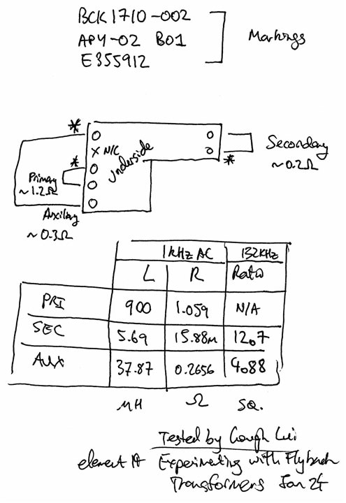
Given that this was for a 5V/2A power supply, or 10W roughly, I would say the 093830 rated at 8W is probably the closest match – it has a secondary ratio of 18.5 compared to 12.7 which would probably mean slightly lower voltage than expected. The auxiliary winding would be substituted with the shield winding which has a ratio of 4 compared to 4.88. Numerically this may seem close but percentage-wise, it is significant.
I can begin to understand why custom-wound transformers are necessary! The transformer itself isn’t a drop-in replacement due to the shape and pin-spacing, so some creativity is required.
For this rather temporary test, I have used hot glue to secure the transformer “dead-bug” style, upside down. Do not try this at home – only trained professionals should attempt such hacks!
From there, using insulated wire, I would wrap around each terminal and solder it, linking using the wire to the PCB to match the required winding order.
The secondary side has both secondary output coils paralleled together in the correct winding order to produce one output of twice the current rating. This is still perhaps slightly less than the original adapter is rated for – but I’d be happy if it just works.
Finally, because it will not fit in its original casing and hence not be able to use its original “pin” contact connections, I found some scrap mains lead from my parts bin and soldered it to the lugs …
The moment of truth has arrived … so I place the unit into a glass jar with the wires led through the lid just in case it pops …
All that work and … it’s an anticlimax! The unit tries to come up but obviously trips some protection or fault on the way up, shuts down and retries. It doesn’t matter what the connected load is doing, it won’t fire up. Is it the higher primary inductance? Or the fact the ratios are all different now? Or something else entirely? Unfortunately, I don’t know … but what I do know is that it doesn’t work and perhaps if this had been an optoisolator feedback type circuit, I might have had a better chance.
Q7: Building a Very Basic Flyback Circuit to Step-Up
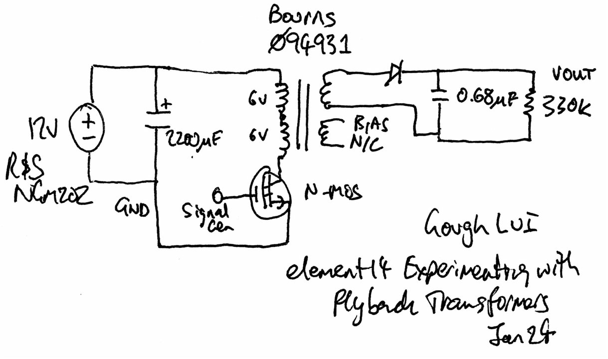
For this experiment, I chose the Bourns 094931 SP-E 20/6 Flyback Transformer. The reason for this is several fold – for one, I wanted to avoid high voltage in my experiments as I couldn’t confidently work with it and switch it quickly with my junk box parts. Remembering that the physics of transformers is (generally) reversible, the distinction in primary and secondary is merely by name. As long as the secondaries were rated at reasonable voltages that I could work with, I could drive them and expect the system to step-up the voltage to something bigger. The 094931 has two 6V/1.8A-rated secondaries, which could be wired in series so I could drive it nicely from 12V.
Another reason for this choice is that generating high voltages from low voltages can be immensely useful. This transformer claims a 19.75 : 2.75 : 1 : 1 ratio, as a result, I would expect, giving 12V to the two 6V windings in series, I would get 19.75 x 6V = 118.5V from the primary. I decided to keep things simple and left the bias winding open, but were I greedy, I could have series this with the primary to get a total of 22.5 : 1 ratio or an expected 135V.
Of course, the simple circuit needs some additional “helpers” – the first being a tanky primary side capacitor. This was mainly just out of concern that the wildly rapidly pulsating current may not play well with my wires and the power supply, even though I chose to use a very competent and fast Rohde & Schwarz NGM202 for this experiment. The second is a rectifying diode for the output, which I chose to use a classic 1N4004 (400V, 1A, 0.7V Silicon) – inexpensive, somewhat fast but perhaps not low-loss. For the capacitor to smooth the output voltage, I used an X2 safety rated capacitor, 0.68uF 250V AC-rated. Being a polyester film capacitor, usually these are pretty tolerant of a bit of overload. Of course, because I didn’t want to get zapped, there had to be a load to quickly discharge the capacitor once power was shut down, so I chose a 330kΩ 1/4W carbon film resistor from the junk box.
The switching element is classically an N-MOSFET and I have not deviated from this. Rummaging through my junk box, I found some Rds Test PCBs I had previously built with certain MOSFETs mounted on them. As a result, I pressed one back into service for this experiment – one containing an ST Microelectronics STP22NF03L (30V, 22A, 50mΩ). I do realise that my “addiction” to low-Rds MOSFETs is unhealthy when it comes to fast switching due to high gate charge/capacitance and reduced breakdown voltages.
To drive this, I would use the onboard signal generator on the Rohde & Schwarz MXO4 Oscilloscope (review pending). As signal generators typically have a source impedance of 50Ω, this is not ideal for quickly changing the gate voltage, but it may still be a good enough drive.
Attempt #1: It Works … Sort-Of.
Setting the signal generator to 132kHz Square Wave, 10V drive with 5V offset (so as to swing between 0V and 10V to drive the gate “hard”) and 50% duty cycle (because it seemed a good value) … I didn’t expect it to work when I applied the power.
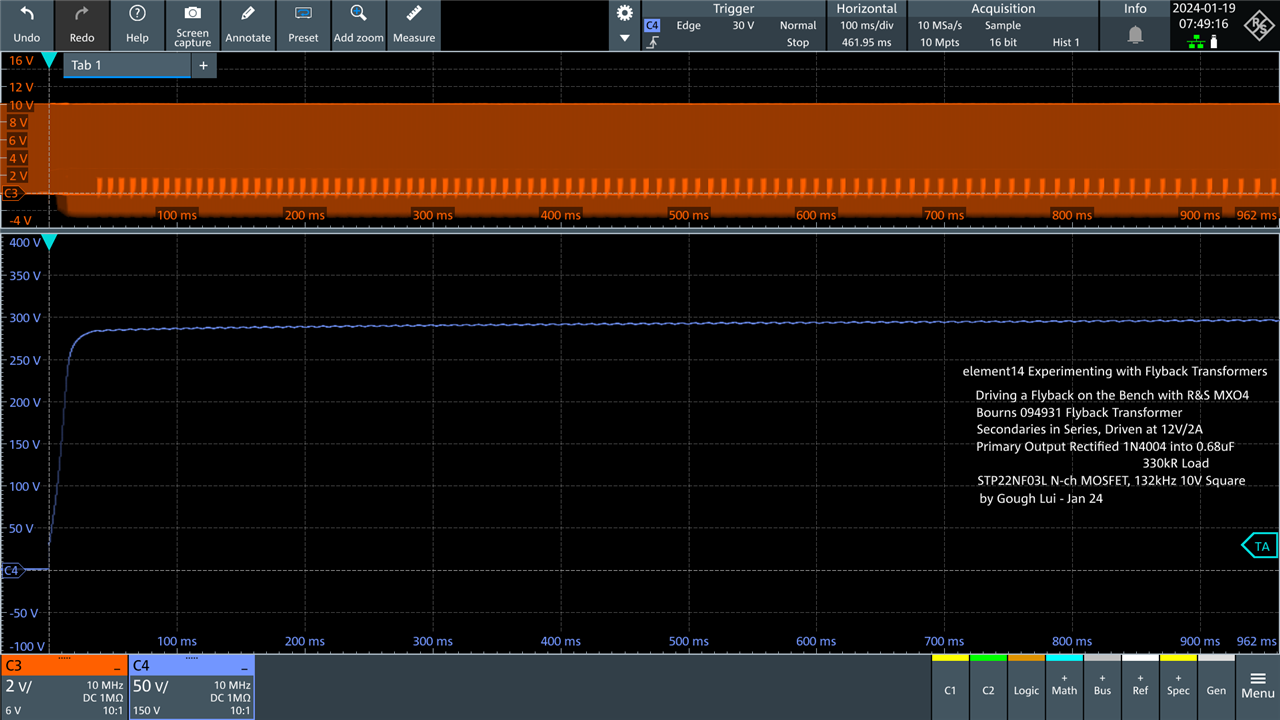
But it did. It created an output voltage just shy of 300V, more than twice what I was expecting. It also seemed to be a bit of a current hog – it was drawing about 1.6A from my supply which seemed a bit much. In these diagrams, C4 (Purple) is the flyback output voltage and C3 (orange) is the gate input voltage.
Overjoyed that something actually happened this time. I turned it off, set my ‘scope up differently and powered it back up again.
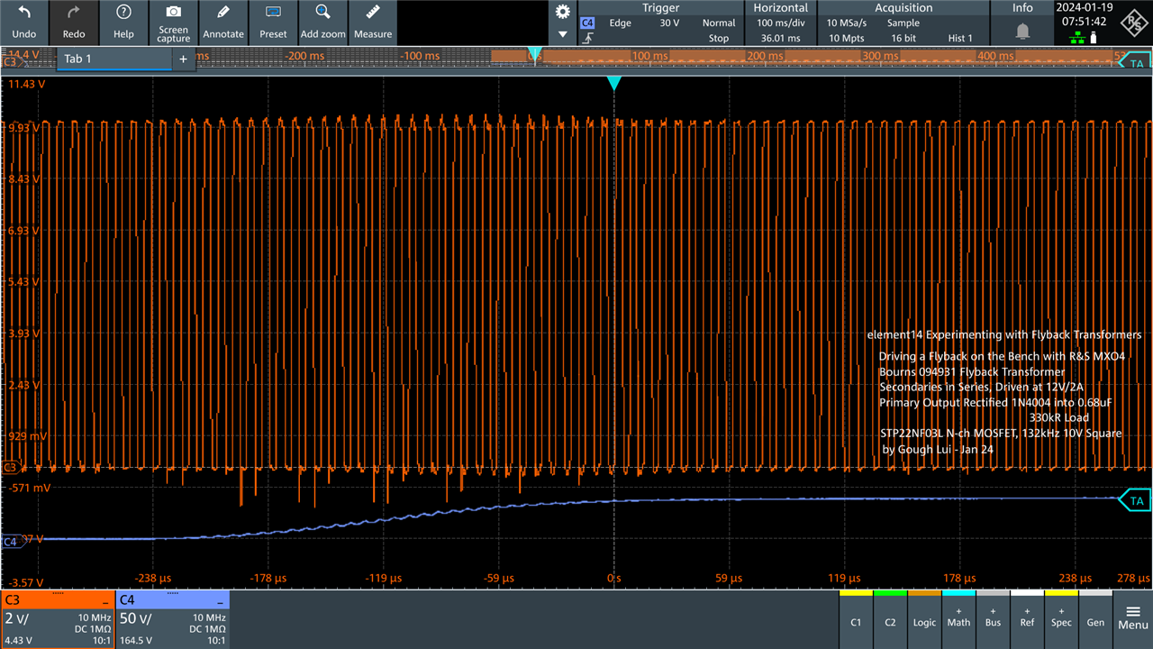
Using a lot of zoom, we can see how it starts up – the voltage does have “ripples” between each pulse, indicating that it is doing what a flyback does – charging the magnetic core through the primary when the MOSFET is turned on and dumping that into the secondary when the MOSFET is opened.
So why is the output voltage higher? I suspect it’s because of inductive kick or perhaps because there is some sort of ringing. But it’s perhaps a nice bonus.
But before I could celebrate and get some more results, it stopped working. Instead, now, it wasn’t showing any of its flyback behaviour and it seemed to be loading the supply a lot more.
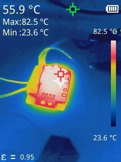
Without thinking, I decided to feel around to see if anything was hot and the MOSFET was literally burning. The tip of my index finger definitely felt it – this thermal image was taken a whole minute afterward.
Attempt #2: I’m Not a Chef. Why Am I Cooking Chips?
One MOSFET down and a few ideas later, I got out the desoldering tool, whipped off the dead MOSFET and chucked in an ST Microelectronics ST55NF06. This time, it’s 60V, 50A, 18mΩ rated with a normal threshold gate that can tolerate 20V absolute maximum. Surely, this uprated MOSFET would be up to the task! I also improved the grounding, providing a direct ground path to the MOSFET independent of the flyback’s ground path to avoid voltage differentials.
I put it into circuit, but then I decided to take off the supply to the flyback just to begin with.
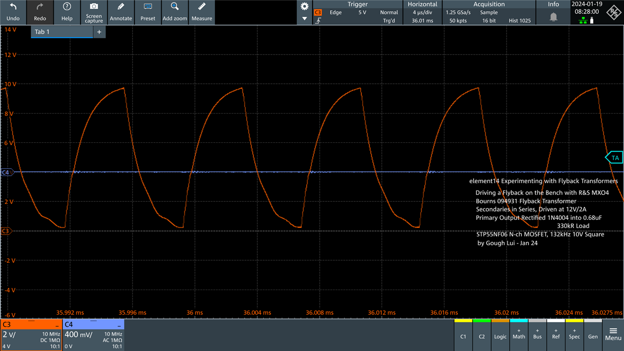
Turns out the gate on this MOSFET is a big one as my signal generator is putting out shark-fins rather than square waves. [Insert expletive of choice].
While the MOSFET may be up to the task, the signal generator is not … and with this kind of slow turn on/off, I can expect only wonky results and perhaps even more dissipation than before.
This is where I should be using a proper gate driver IC. I tried looking for my Infineon 1EDN8550B Gate Driver from a previous RoadTest but cannot locate the evaluation board. A second-best would probably be to use an opamp as a voltage follower and have that “buffer” the signal generator output and provide the bulk of the current. The problem? I don’t have many opamps on hand that can handle 10V+ and the ones that I do are slow with GBP of 1MHz and slew rates no more than about 5V/µs. The best I had was an OPA990 which I soldered onto a breakout and powered from the same 12V bus as the flyback itself …
… but this resulted in a more trapezoid waveform.
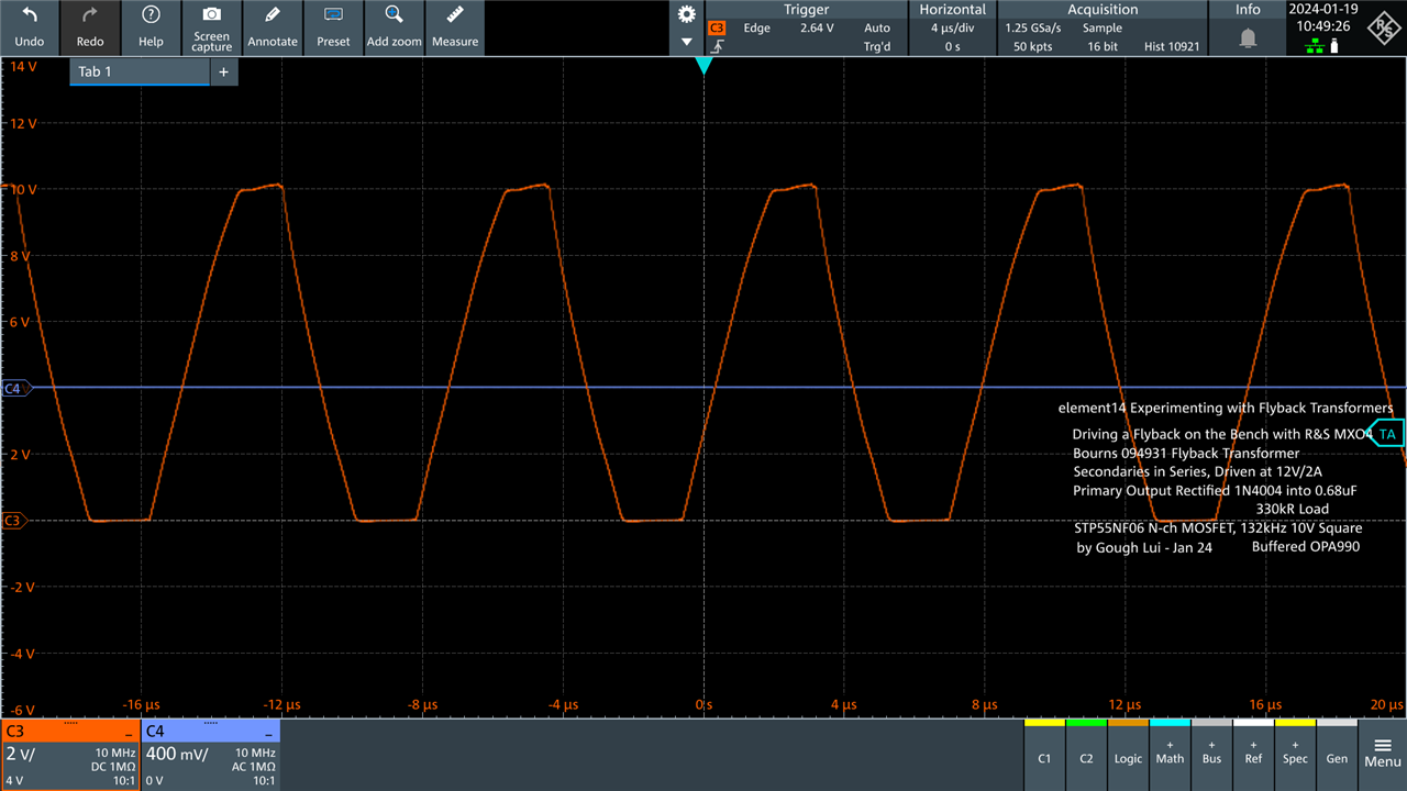
At least it looked somewhat nicer … even if it is slow. I guess I won’t have to be concerned about potential for dV/dT failures of MOSFETs with such a slow gentle waveform, but instead dissipation and linear-region operation is the concern instead.
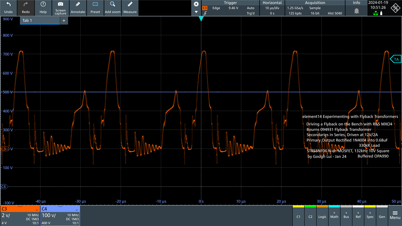
After plugging in the flyback, the gate waveform now looks very strange indeed. At a duty cycle of 50%, I’m now getting 500V on the output – I wonder if this is because the capacitor itself is “leaking” enough to balance the voltage out or whether it’s the 1N4004 reaching its true limit (400V rated, likely with some headroom) and breaking down, but not passing enough energy to actually harm itself. This is a very suspicious number to arrive at.
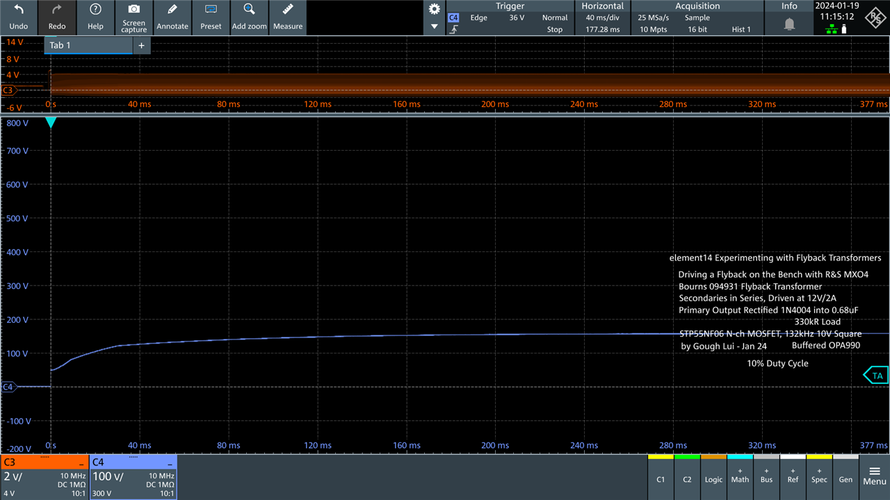
Reducing the duty cycle to 10% dropped the voltage to a more manageable 160V or so. As a result, it seems we have been able to show the use of duty cycle to control the transferred energy and thus, regulate the voltage (assuming you have some feedback and a controller that can modulate the duty cycle).
Not long after this … this MOSFET perished as well, as I was not taking care of the heat while gawking at the results and trying repeatedly to get meaningful oscilloscope captures.
Attempt #3: Still Getting More Than I Bargained For!
I’m not made of money but my junk box has more to give. This time, for better or for worse, I decided to see whether life would be easier with a International Rectifier IRFZ34E, a rather long-lived product with ratings of 60V, 28A, 42mΩ. I’m just hoping that this one might be a bit less of a gate capacitance issue.
To ensure its longevity, I caved and decided to use a USB fan, powered by a powerbank, to give a bit of forced convective cooling. It may be cheating, in a sense, but I need my results and time’s running out!
I’ve also added a high-voltage differential probe (HVP-70) to measure between the secondary windings (driven with 12V) to understand better what is happening at least with the voltage. I don’t have any current probes though. In the following diagrams, C4 (Purple) is the flyback output voltage, C3 (orange) is the gate input voltage and C2 (green) is the voltage across the flyback input winding.
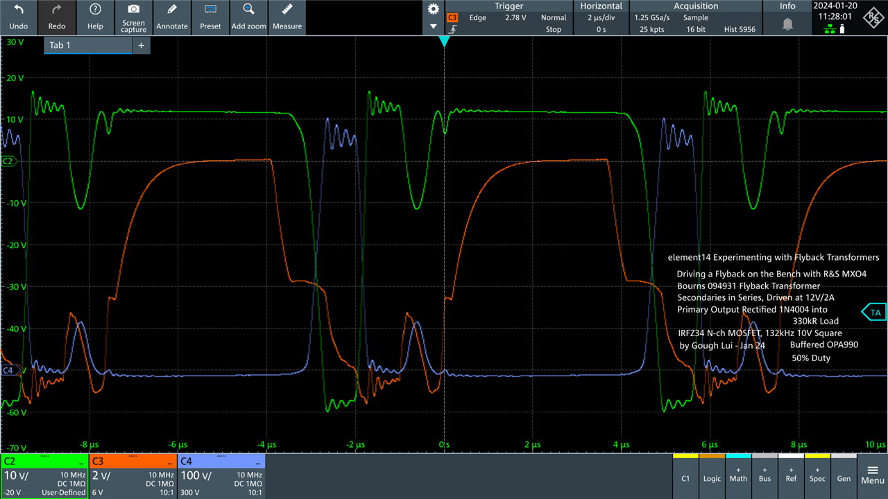
I removed the output capacitor to see how the circuit is really behaving. Looking at the flyback input voltage in green, we can see that flyback action is actually happening. The trigger point is when the MOSFET is turned on, and the coil is nicely charging at 12V. As the MOSFET turns off (somewhat delayed), the input coil drops negative and the output coil “flies” back to a much higher voltage – in this case, we’re seeing about 600V peak! Part of this is winding ratio, but the other may be some kind of resonance (with the ringing) and inductive “kick”, but I’m not entirely sure. This “flyback” action on the output coil only lasts a while until the field seemingly collapses and then the input coil voltage “flies up” again with a seemingly bigger ring before the cycle begins itself anew.
Looking at this, I am somewhat confused. I didn’t realise that during the flyback, the primary voltage would get so negative, even if briefly. I would expect the MOSFET’s body diode to conduct in about 100ns which I would have imagined would short it out if the coil developed a negative voltage. Considering this “peak” – if it were real, would have resulted in 1185V on the secondary by pure ratio – but perhaps the 330kΩ load dragged this down to the ~600V peak observed. The ringing is quite an interesting phenomenon – perhaps it’s affecting the ground enough that the MOSFET’s actually getting to the point of a partial turn-on during one of the rings. Maybe the faster edges in some cases were provoking more severe ringing, heating up and killing the MOSFETs quicker.
At this point, seeing the voltages are approaching 600V, I wondered if it’s the 1N4004 that’s letting me down. I decide to replace it with two 1N4004’s in series for a total of 800V to see if the output voltage would rise – it didn’t. I wonder if increasing the MOSFET’s Vds breakdown rating would help there or whether it’s something else entirely (perhaps the Q of the transformer itself).
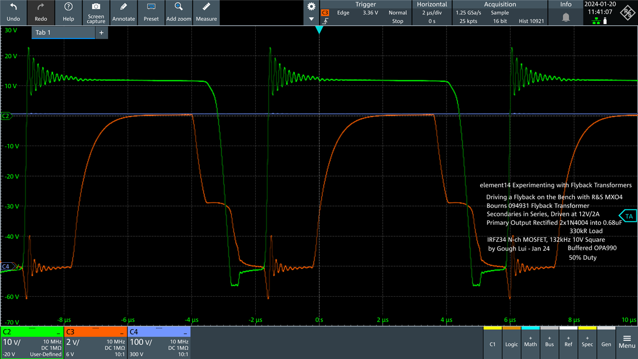
Here’s the same test with the output capacitor connected – the ringing is quite a bit cleaner to see and the nature of the ringing is different. Perhaps this is removing the secondary ringing from reflecting back into the primary.
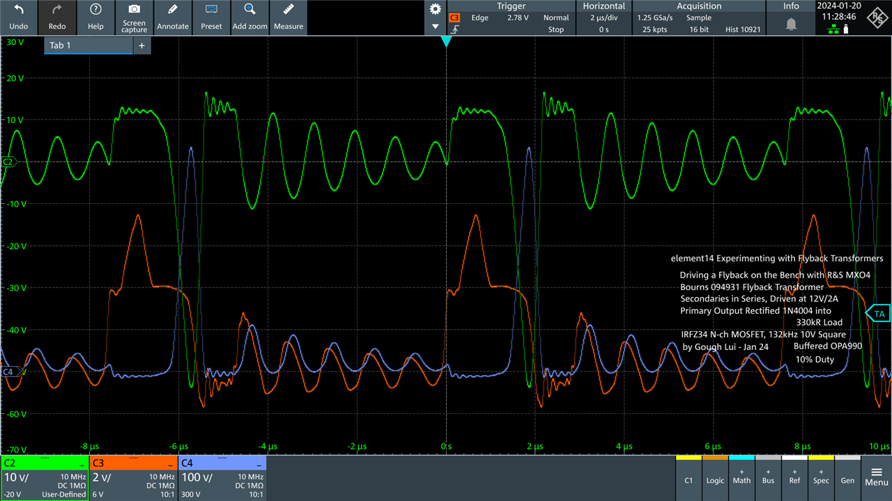
Dropping the duty cycle to 10% seems to show the ringing behaviour more clearly, with two different ringing frequencies observed. The voltage spike is more like 530V now, but for a shorter time, which when smoothed by a capacitor, results in a lower (average) voltage.
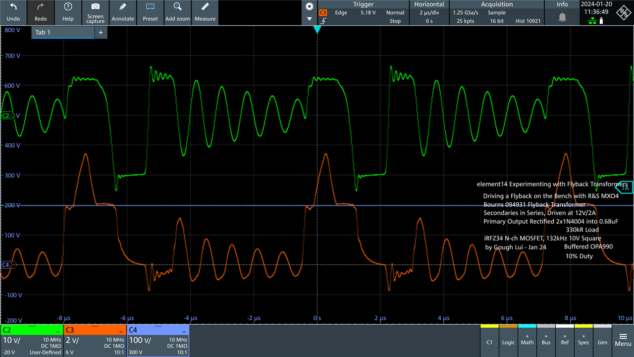
Here’s the same test with the capacitor plugged in. The waveform differs subtly when the output is smoothed – it seems less secondary ringing means less secondary ringing being inducted into other parts of the system. Overall, I would consider this experiment a success, even if it was rudimentary.
Q8: What’s Missing from a Practical Design?
I think it should be quite obvious that most simple circuits are not practical circuits in real life. For one, such a circuit has ignored the need for regulation. In a practical use, the output voltage is usually regulated to a constant value even in the face of varying loads. In order to do this requires adjusting duty cycles or even skipping pulses under light loads (if energy efficiency is to be concerned). This is usually done with a flyback controller IC to automate the control aspects. Regulation would entail sensing the output voltage and feeding this back safely, which in traditional designs would rely on an optocoupler. In newer designs, there is the potential to use primary side sensing as an alternative (as the cheap Chinese USB power supplies seem to have used). Each has their own regulation benefits and complexity drawbacks, but it is important that isolation is maintained in this feedback system to ensure the isolation benefit of the flyback transformers can be fully realised.
Another issue that isn’t discussed is simply the EMI potential as many different frequencies are being generated in this circuit that can possibly be emitted along connecting wires and cause interference to other electronic devices. This is where the use of the common-mode choke can help, along with various design features to reduce the likelihood of emissions (e.g. bypass capacitors, snubbers and ferrite beads).
Of course, a big contributor to that (and the issues observed above) is the ringing itself. A proper way of dealing with the ringing would be to use a RCD snubber, as recommended in this Analog Devices Inc Technical Article and this Fairchild Application Note AN-4147. The use of a well-calculated resistor, capacitor and diode will allow for absorbing just the surge voltage in each cycle, while reducing energy losses. Unfortunately, this is beyond my current level of understanding and outside the time available for me to implement – but it’s nice to be aware of the proper way to solve the issue and the types of resonances that cause it.
There is also the issue of circuit protection in case anything goes wrong – for example, an appropriately rated fuse in case the switching element gets stuck closed (or is blown shorted).
Q9: The Final Push – Another Modification Attempt with a Boost Module Instead
I wasn’t entirely satisfied with a lack of regulated flyback action, so thanks to a comprehensive comment by jc2048 on Part 5, I decided to give it one more go but this would be my absolute last given the time I have available.
Remember that the flyback topology resembles a boost converter with a transformer instead of an inductor? That gave me an idea which was so obvious in hindsight, I’m surprised I didn’t try it first. I got out one of these rather popular MT3608 boost converter modules as the basis for a bit of modification. This is not an ideal module to be using as the IC switches at 1.2MHz, which is quite a lot higher than the 132kHz the transformer is optimised for, but I had none of the older variety which switched at 400kHz in my junk box.
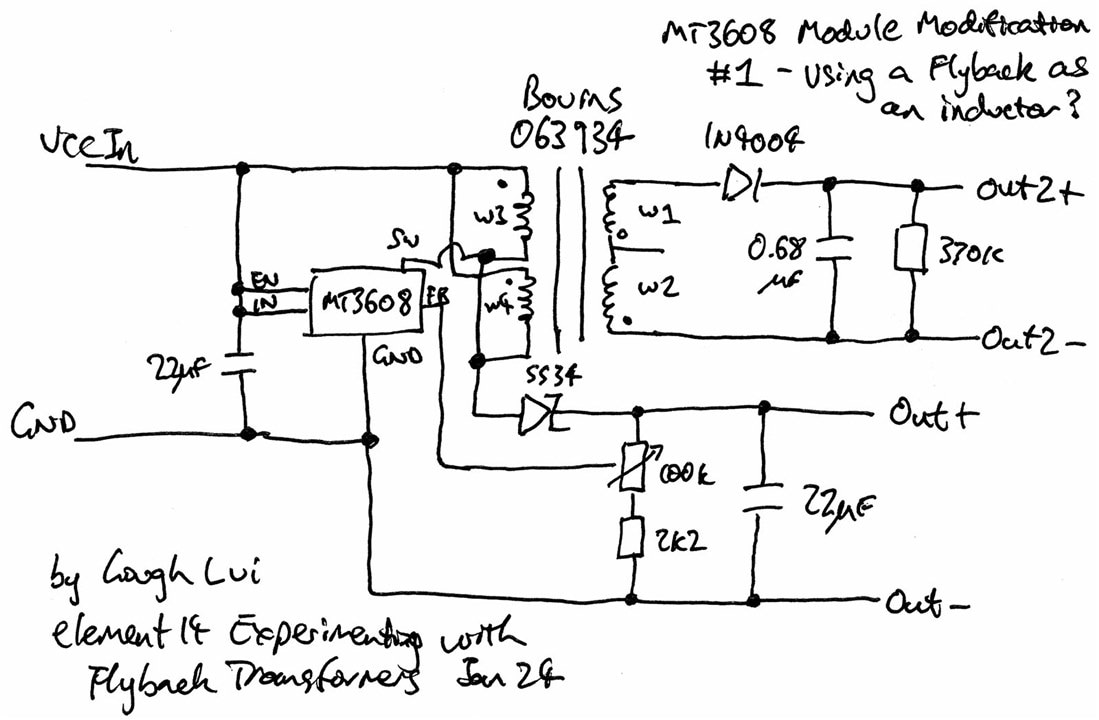
The proposed “step one” would be simple – remove the inductor and replace it with the secondaries (in parallel) of a Bourns 063934. Changing nothing else, I was hoping that in spite of the difference in inductance and the high operating frequency, that the unit was still able to run as an ordinary boost converter just with a “second rail” consisting of the primary and bias windings in series, which may be at a higher voltage. I didn’t know what would happen to it – would there be some regulation? Likely not because the feedback was not on this second rail.
With some creative soldering and solid core wire, I was able to realise this configuration for testing.
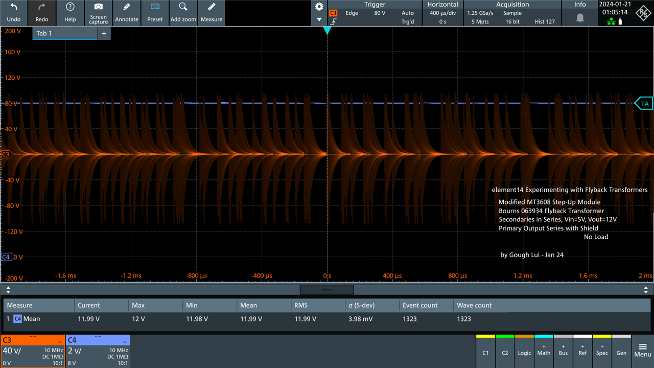
To my surprise, when I fed the module with 5V and adjusted the potentiometer, it was working as a boost converter and giving a nice 12V output on its main output. The second rail, in orange, was showing the converter was operating in some sort of low-power hiccup mode, with ringing pulses peaking around 110V. That sounds about right …
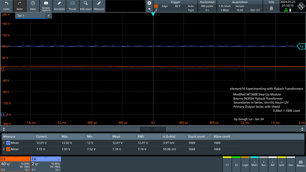
Putting a diode, capacitor and resistive load on it, however, dragged the rail down to about 7-8V. A far cry from what I expected. I suppose this is what happens when you only load one of multiple-rails in a flyback system.
Now that I can see this working, I decided to take one more step – let’s move the feedback to the second rail consisting of the primary and bias windings in series. To do this, I would modify the PCB by removing the rectifier diode and then patching in the feedback potentiometer and resistor to the positive side of the second rail. The negative side would be commoned to ground.
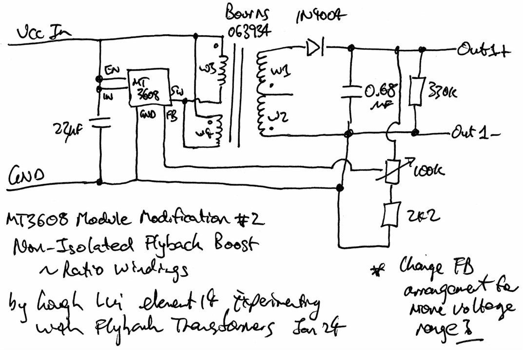
This would make a non-isolated converter which eliminates a key benefit of the flyback transformer, but it should still work in theory.
A little more creative soldering and it’s been built.
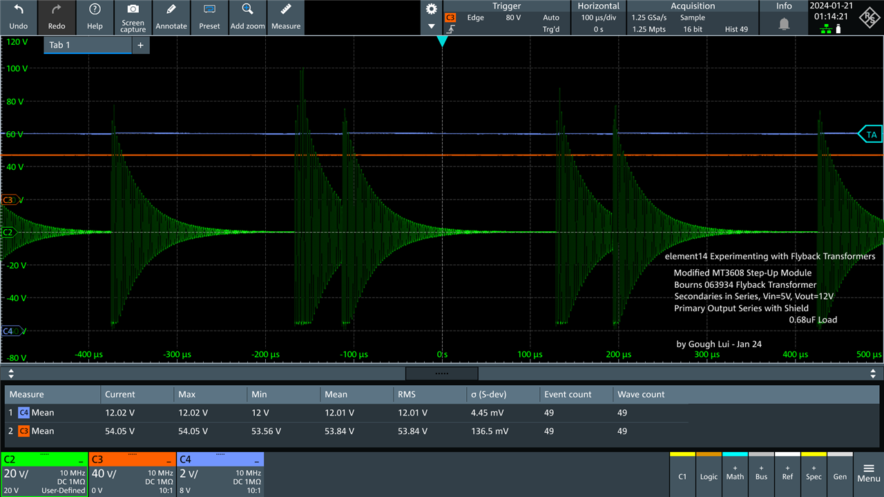
Powering up, the output from the other side of the transformer was rock-solid at the 12V that it was previously set to indicating the circuit was indeed regulating the output. I was able to dial it up to about 30V (the original maximum voltage) because of the way the voltage divider was set but after a short time, the MT3608 died a dead short …
This is when I decided to take a look back at the difference between schematics – hmm, originally the normal output goes through a Schottky diode, a capacitor filter in-parallel with a resistor trimpot for feedback. Aha! That network, while not intended to be, actually acted as a RCD snubber it would seem, which is why the circuit didn’t blow up initially. Once I removed the Schottky to move the feedback around, that removed whatever snubbing effect it may have had, which probably overstressed the internal MOSFET.
Knowing this, I tried building a separate snubber network with different values, replacing the MT3608 and adding resistance to the divider network to allow for higher regulated output voltages, but it just chose to blow right away every time even with a 5V input. In my haste, I changed multiple variables at once, which is bad science. I am a component murderer … but at least there wasn’t any smoke or physical injury this time. But alas, it seems a few minutes of flyback action is all I can muster for now. That's the end of my weekend!
Conclusion
Thanks to element14 and Bourns for selecting me as one of the challengers for the Experimenting with Flyback Transformers Design Challenge. I hope you’ve enjoyed the journey, even if it was a little rushed and I wasn’t quite as successful as I would have liked. Considering I had never laid hands on a flyback transformer nor understood what the flyback topology was before I started, this has been a valuable opportunity to learn a little along the way.
The flyback topology is conceptually simple, although this is perhaps somewhat misleading when one considers EMI, efficiency and feedback concerns. Nevertheless, it is a popular topology for smaller power supplies of <100W and <10A. The Bourns flyback transformers featured are standard parts which are widely distributed, imbued with Kaschke’s know-how and expertise, making it easier for more designers to benefit without the need for large custom orders needing a certain amount of lead time. In supporting this, there are also matching common-mode chokes in the Bourns catalog. Not having quite the confidence, expertise or time to build something entirely from scratch for high-voltage, I mainly dabbled in modifications and rudimentary circuits which mostly ended poorly, but not because of any fault of the products themselves. In the process, I got to learn what I don’t know, which is a lot … admittedly.
Not being shy of drawing a bit of an analogy twisted with a pun, I end this challenge feeling like some of the unnamed experimenters in the early days of powered flight. While everyone knows the success of the Wright Brothers, my achievements pale in comparison and may soon be forgotten. In all, I managed to fly(back) for all of a few minutes, before plummeting back to the ground (voltage) … cooking chips along the way. As they say, “takeoffs are optional, but landings are mandatory” and in this case, there’s been a few hard landings. Nevertheless, befitting of a series about Flybacks from the Ground Up, that we end it back on ground safely after accidentally generating ~500V DC on the bench.


Top Comments