The TDC1000-TDC7200EVMTDC1000-TDC7200EVM evaluation module has 4 main parts The TDC1000 analog front-end and a pre-programmed MSP430 microcontroller on the board, a 1MHz Piezo Ceramic sensor that plugs into the board and a GUI client for on your PC.
In this blog I'm tapping into the SPI traffic.
a
a |
SPI Traffic and Bodging the Board
The evaluation board has some interesting SPI communication going on. The ultrasonic sensing ic TDC1000 is configured by it, and you can get at the config and measurements of the fancy timer chip TCD7200.
image edited from TDC1000 | Ultrasonic Analog Front End | Ultrasonic Sensing | Online datasheet
Although the communication with the TDC7200 may be more exciting to monitor - we'd be able to see values change when water levels change - I'm focusing on what's sent back and forth between the on-board microcontroller and the TDC1000.
Getting at the Signals
It's not too difficult to get at 3 of the 4 SPI signals. There are test points on the board to get at the SCLK, MOSI and MISO.
These test points are not populated, so my first action was to solder in male headers.
I initially thought that I could get away without breaking out the CS. But the traffic that I could tap off was containing info for the TDC1000 and TDC7200 intermixed.
Because my logic analyzer has limitations, I couldn't define a nice trigger point to isolate TDC1000 traffic from the stream.
The only way - with my limited setup - to sample TDC1000 traffic, was to hack myself access into the CS signal.
That meant scraping off the solder mask of a tiny trace on the bottom layer, and soldering a thin wire onto that.
I used an open via to bring the wire to the front side, and secured the bodge with some tape at the underside.
I've marked the connection points on the drawing below.
Sampling the SPI Data
My logic analyzer is a Papilio that's configured as an OpenLogic compatible device (see Make a Logic Analyzer from your Dev Kit Part 2: Papilio FPGA).
I connected all four SPI signals to the inputs of the LA.
| SPI signal | Test point | Colour | analyzer input |
|---|---|---|---|
| SCLK | TP19 | orange | 0 |
| MOSI | TP20 | white | 1 |
| MISO | TP21 | blue | 2 |
| CS | bodge wire | yellow | 3 |
Once that was done, I set up my sample on the falling edge of the CS. So I started collecting data as soon as the chip select was pulled low (active).
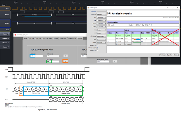
On the images that follow, you can see the activity of a read and a write operation to the register on address 0x01.
We select read or write by setting bit 6 of the command field to 0 or 1. The address that is read or written is determined by bit 0 to 5.
Reading from address 0x01
In this exercise, we'll send a SPI command to read address 0x01. In binary, we're sending 00000001.
0: read
000001: address 0x01.
Since this is a read operation, the value should come to us in the second 8 bits burst via the MISO (slave TDC1000 tells us the value of the Config-1 register).
You can see on the GUI, signal display and protocol analyzer that we're retrieving 0x40.
Writing to address 0x01
In this exercise, we'll send a SPI command to write to address 0x01. In binary, we're sending 01000001.
1: write
000001: address 0x01.
Since this is a write operation, we have to send the value in the second 8 bit burst via the MOSI ( we tell slave TDC1000 to write it into the Config-1 register).
The MISO line doesn't play a role in this scenario because the slave doesn't send any data. It is flat on the sample below.
You can see on the GUI, signal display and protocol analyzer that we're writing 0x40.
That's it for today. With a few changes to the kit you have access to the communication between the main players on the board.


Top Comments