element14 Community
element14 Community
    Register Log In
  • Site
  • Search
  • Log In Register
  • Community Hub
    Community Hub
    • What's New on element14
    • Feedback and Support
    • Benefits of Membership
    • Personal Blogs
    • Members Area
    • Achievement Levels
  • Learn
    Learn
    • Ask an Expert
    • eBooks
    • element14 presents
    • Learning Center
    • Tech Spotlight
    • STEM Academy
    • Webinars, Training and Events
    • Learning Groups
  • Technologies
    Technologies
    • 3D Printing
    • FPGA
    • Industrial Automation
    • Internet of Things
    • Power & Energy
    • Sensors
    • Technology Groups
  • Challenges & Projects
    Challenges & Projects
    • Design Challenges
    • element14 presents Projects
    • Project14
    • Arduino Projects
    • Raspberry Pi Projects
    • Project Groups
  • Products
    Products
    • Arduino
    • Avnet & Tria Boards Community
    • Dev Tools
    • Manufacturers
    • Multicomp Pro
    • Product Groups
    • Raspberry Pi
    • RoadTests & Reviews
  • About Us
    About the element14 Community
  • Store
    Store
    • Visit Your Store
    • Choose another store...
      • Europe
      •  Austria (German)
      •  Belgium (Dutch, French)
      •  Bulgaria (Bulgarian)
      •  Czech Republic (Czech)
      •  Denmark (Danish)
      •  Estonia (Estonian)
      •  Finland (Finnish)
      •  France (French)
      •  Germany (German)
      •  Hungary (Hungarian)
      •  Ireland
      •  Israel
      •  Italy (Italian)
      •  Latvia (Latvian)
      •  
      •  Lithuania (Lithuanian)
      •  Netherlands (Dutch)
      •  Norway (Norwegian)
      •  Poland (Polish)
      •  Portugal (Portuguese)
      •  Romania (Romanian)
      •  Russia (Russian)
      •  Slovakia (Slovak)
      •  Slovenia (Slovenian)
      •  Spain (Spanish)
      •  Sweden (Swedish)
      •  Switzerland(German, French)
      •  Turkey (Turkish)
      •  United Kingdom
      • Asia Pacific
      •  Australia
      •  China
      •  Hong Kong
      •  India
      •  Japan
      •  Korea (Korean)
      •  Malaysia
      •  New Zealand
      •  Philippines
      •  Singapore
      •  Taiwan
      •  Thailand (Thai)
      •  Vietnam
      • Americas
      •  Brazil (Portuguese)
      •  Canada
      •  Mexico (Spanish)
      •  United States
      Can't find the country/region you're looking for? Visit our export site or find a local distributor.
  • Translate
  • Profile
  • Settings
FPGA
  • Technologies
  • More
FPGA
Blog Cheap Cyclone 10
  • Blog
  • Forum
  • Documents
  • Quiz
  • Events
  • Polls
  • Files
  • Members
  • Mentions
  • Sub-Groups
  • Tags
  • More
  • Cancel
  • New
Join FPGA to participate - click to join for free!
  • Share
  • More
  • Cancel
Group Actions
  • Group RSS
  • More
  • Cancel
Engagement
  • Author Author: michaelkellett
  • Date Created: 31 Jul 2021 2:28 PM Date Created
  • Views 5705 views
  • Likes 15 likes
  • Comments 24 comments
  • fpga design
  • vhdl
  • altera
Related
Recommended

Cheap Cyclone 10

michaelkellett
michaelkellett
31 Jul 2021

I've been following the discussions about the VIDOR4000 in the FPGA group. There was a giveaway associated with the Webinar but of course there will be sonme disapointed non-winners.


If you want to get into playing with FPGAs one of the cheapest routes I've found so far is to buy a simple dev board from Aliexpress. There are lots avaialble but this blog is about the Cyclone 10

board from QMTech.

https://www.aliexpress.com/item/1000006634063.html?gps-id=pcStoreJustForYou&scm=1007.23125.137358.0&scm_id=1007.23125.13…

I paid about £16 for mine. I already have a "ByteBlaster" programmer but if you don't it will cost about another £10.


The free version of Altera Quartus will do for development.


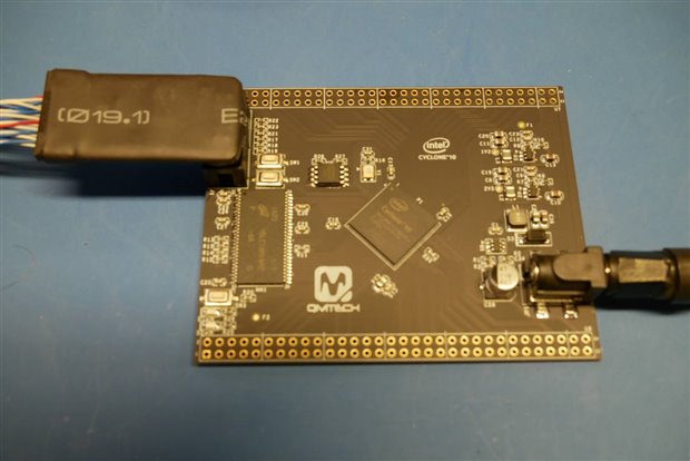
The Cyclone 10 FPGA on this board is smaller than the one on the Vidor board with only about 6k logic elements - but that's enough for useful work.
 

image


The board has a 50MHz clock oscillator, a boot Flash chip and a 32MByte SDRAM and the usual regulators for the supply. It comes with a resaonable set of examples which are

extermely useful in getting it running. I downloaded Version 17.1 of Quartus from Intelto match the version used on the board examples. I've also downloaded the 20.1 version for

my own stuff. Running FPGA designs on different versions of the tools often causes problems - so it's best avoided if you can.

The examples are all in Verilog.


There's a good blog from  jc2048   at VIDOR 4000: Servo Interface where we have had some discussions about VHDL coding (style and substance image) and a thing that came up

was the possibility of using standard VHDL to infer Block Rams on the FPGA. (The other way is to explicitly refer to the block ram using special IP blocks specific to the FPGA vendor).


Having got the LED flasher Verilog demo translated to VHDL I've added a chunk of RAM to the design. It doesn't have anything to do right now so to stop the tools  optimising it away

I've connected it to pins. (Which takes me to another big virtue of the QMTech board, it has about 100 IO pins available on its headers.)


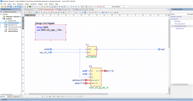
This a block diagram of the project. It's done in Aldec-HDL. It's a complete VHDL/Verilog simulator (and more). The block diagram automatically makes all that boring VHDL or Verilog

that links blocks together. The actual code is inside the blocks. I find it helps a great deal to visualise a complex project and saves a lot of time. It isn't free.
 

image


This is the RAM code:


library IEEE;
use IEEE.std_logic_1164.all;   
use IEEE.NUMERIC_STD.all;


entity mem_inf_sp_64_12 is
     port(
         we : in STD_LOGIC;
         en : in STD_LOGIC;
         clk : in STD_LOGIC;
         address : in STD_LOGIC_VECTOR(5 downto 0);
         data : in STD_LOGIC_VECTOR(11 downto 0);
         q : out STD_LOGIC_VECTOR(11 downto 0)
         );
end mem_inf_sp_64_12;

--}} End of automatically maintained section

architecture mem_inf_sp_64_12 of mem_inf_sp_64_12 is   

    type ram_type is array (0 to 63) of std_logic_vector(11 downto 0);   -- array must be 0 - n, if declared the other way wit downto to match Xilinx example then Quartus fitter fails
    signal ram : ram_type;

begin

    process(clk)
    begin
        if rising_edge(clk) then
            if en = '1' then
                if we = '1' then
                    ram(to_integer(unsigned((address)))) <= data;
                end if;
                q <= ram(to_integer(unsigned((address))));
            end if;
        end if;
    end process;

end mem_inf_sp_64_12;


All pure VHDL but note that comment on line 21 - my Xilinx example codes the array "63 downto 0" - I don't have a Xilinx toolset runing so I can't test if they care, but the Altera tools

only infer the block memory one way round.

(There seem to be some extra brackets in lines 31 and 33  - but they do no harm)
 

image


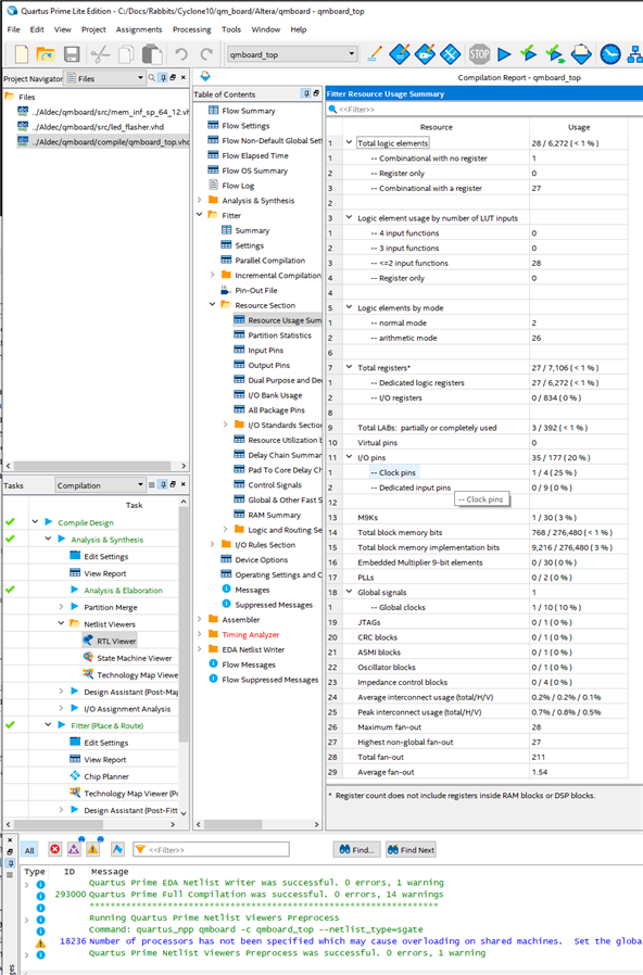
The screenshot shows the loveliness of the Altera toolset and the resources used


So there you go -  a really cheap (and by FPGA standards, a quite simple) way into FPGA.


QMTech do a very similar board (but about twice the price) with an Artix 35 on it - I'll attempt to repeat this experiment when it turns up.


MK

  • Sign in to reply

Top Comments

  • michaelkellett
    michaelkellett over 5 years ago in reply to 14rhb +5
    Happy to share ! If anyone buys one of these and needs to talk about I'll (almost always) respond on E14. I suppose I should point out that I have no connection with Aliexpress or QMTech. Just trying to…
  • 14rhb
    14rhb over 5 years ago +4
    When trying to learn electronics on a small budget it can be a difficult decision whether to pay out for a reputable dev board or to opt for a low-cost one via the route you have identified. Therefore…
  • dang74
    dang74 over 5 years ago +4
    Thank you Michael, Three years ago I purchased a Cyclone IV board made by QMTECH. It is the same form factor as your board. I don't remember the exact price but it was very inexpensive and I've put it…
Parents
  • Jan Cumps
    Jan Cumps over 5 years ago

    I'll check if the (inverse) array declaration gives issues in Xilinx.


    image

    The validator doesn't complain, but I still have to go through the steps...

    • Cancel
    • Vote Up +2 Vote Down
    • Sign in to reply
    • More
    • Cancel
  • Jan Cumps
    Jan Cumps over 5 years ago in reply to Jan Cumps

    Use after place design:

    1. Slice Logic
    --------------
    +----------------------------+------+-------+-----------+-------+
    |          Site Type         | Used | Fixed | Available | Util% |
    +----------------------------+------+-------+-----------+-------+
    | Slice LUTs                 |  498 |     0 |     53200 |  0.94 |
    |   LUT as Logic             |  426 |     0 |     53200 |  0.80 |
    |   LUT as Memory            |   72 |     0 |     17400 |  0.41 |
    |     LUT as Distributed RAM |   12 |     0 |           |       |
    |     LUT as Shift Register  |   60 |     0 |           |       |
    | Slice Registers            |  741 |     0 |    106400 |  0.70 |
    |   Register as Flip Flop    |  741 |     0 |    106400 |  0.70 |
    |   Register as Latch        |    0 |     0 |    106400 |  0.00 |
    | F7 Muxes                   |    0 |     0 |     26600 |  0.00 |
    | F8 Muxes                   |    0 |     0 |     13300 |  0.00 |
    +----------------------------+------+-------+-----------+-------+

    ...

    3. Memory
    ---------
    +----------------+------+-------+-----------+-------+
    |    Site Type   | Used | Fixed | Available | Util% |
    +----------------+------+-------+-----------+-------+
    | Block RAM Tile |    0 |     0 |       140 |  0.00 |
    |   RAMB36/FIFO* |    0 |     0 |       140 |  0.00 |
    |   RAMB18       |    0 |     0 |       280 |  0.00 |
    +----------------+------+-------+-----------+-------+


    Looks like no custom RAM is used.

    Some things were optimised out later on, by combining LUTs:


    -------------------------------------------------------------------------------------------------------------------------
    |  Phase                        |  #Cells created  |  #Cells Removed  |  #Constrained objects preventing optimizations  |
    -------------------------------------------------------------------------------------------------------------------------
    |  Retarget                     |               4  |              29  |                                              0  |
    |  Constant propagation         |               0  |               8  |                                              0  |
    |  Sweep                        |               0  |             169  |                                              0  |
    |  BUFG optimization            |               0  |               0  |                                              0  |
    |  Shift Register Optimization  |               0  |               0  |                                              0  |
    |  Post Processing Netlist      |               0  |               0  |                                              0  |
    -------------------------------------------------------------------------------------------------------------------------

    ...

    Summary of Physical Synthesis Optimizations
    ============================================
    -----------------------------------------------------------------------------------------------------------------------------------------------------------
    |  Optimization                                     |  Added Cells  |  Removed Cells  |  Optimized Cells/Nets  |  Dont Touch  |  Iterations  |  Elapsed   |
    -----------------------------------------------------------------------------------------------------------------------------------------------------------
    |  LUT Combining                                    |            0  |              6  |                     6  |           0  |           1  |  00:00:00  |
    |  Very High Fanout                                 |            0  |              0  |                     0  |           0  |           1  |  00:00:00  |
    |  DSP Register                                     |            0  |              0  |                     0  |           0  |           0  |  00:00:00  |
    |  Shift Register to Pipeline                       |            0  |              0  |                     0  |           0  |           0  |  00:00:00  |
    |  Shift Register                                   |            0  |              0  |                     0  |           0  |           0  |  00:00:00  |
    |  BRAM Register                                    |            0  |              0  |                     0  |           0  |           0  |  00:00:00  |
    |  URAM Register                                    |            0  |              0  |                     0  |           0  |           0  |  00:00:00  |
    |  Dynamic/Static Region Interface Net Replication  |            0  |              0  |                     0  |           0  |           1  |  00:00:00  |
    |  Total                                            |            0  |              6  |                     6  |           0  |           3  |  00:00:00  |
    -----------------------------------------------------------------------------------------------------------------------------------------------------------


    The whole sequence ran without complaining about the array declaration. Loading the bitstream now and I'll try to write and read RAM.

    • Cancel
    • Vote Up 0 Vote Down
    • Sign in to reply
    • More
    • Cancel
  • Jan Cumps
    Jan Cumps over 5 years ago in reply to Jan Cumps

    Not perfect yet image


    image


    I have it working for address 0, others give garbage. Back to the study table


    edit: fixed. It is something with my python wrapper. below is the result of writing to 64 memory addresses, then reading them:


    image


    image


    The array declaration didn't make a difference. I tested with both type ram_type is array (0 to 63)  and type ram_type is array (63 to 0).

    I did not change anything in the VHDL code of the original post above.

    • Cancel
    • Vote Up 0 Vote Down
    • Sign in to reply
    • More
    • Cancel
  • michaelkellett
    michaelkellett over 5 years ago in reply to Jan Cumps

    Hello Jan Cumps ,


    Thanks for the work !


    I think that perhaps your meory array is too small for the Xilinx tools to give it a whole block of ram.


    The 7 series architecture in your Zynq FPGA is good (better than Cyclone 10) at using fabric logic and ram as RAM an I suspect that the memeory array

    is being made like this:

    image


    In the Xilinx tool output:


    1. LUT as Memory            |   72 |     0 |     17400 |  0.41 | 
    2. |     LUT as Distributed RAM |   12 |     0 |           |       | 
    3. |     LUT as Shift Register  |   60 |


    The 12 LUTs would give you a 64 x 12 memory array - and it uses a trivial amount of your FPGA.


    If you can be bothered it would be nice to see what happens if the array is 1024 x 12


    MK

    • Cancel
    • Vote Up +1 Vote Down
    • Sign in to reply
    • More
    • Cancel
  • Jan Cumps
    Jan Cumps over 5 years ago in reply to michaelkellett

    I'm testing with 1024 addresses (11 bit because I can't count image - one address bit too much, but the array is 1024 * 12 data bits).

    I've moved everything related to the ARM controllers in the dark blue box, to simplify the image.

    Here are the interfaces to the memory:


    image


    The green block is the original Memory VHDL, with the address changed to to 11 bits and the array to size 1024

    image


    VHDL changes lines:


    entity mem_inf_sp_1024_12 is
    --
             address : in STD_LOGIC_VECTOR(10 downto 0);
    --
    end mem_inf_sp_1024_12;
    --
    architecture mem_inf_sp_1024_12 of mem_inf_sp_1024_12 is   
    --
        type ram_type is array (0 to 1023) of std_logic_vector(11 downto 0);   -- array must be 0 - n, if declared the other way wit downto to match Xilinx example then Quartus fitter fails
    --
    end mem_inf_sp_1024_12;


    Reported fabric use after full generation.

    This is the Place Design phase's utilisation report


    1. Slice Logic
    --------------
    +----------------------------+------+-------+-----------+-------+
    |          Site Type         | Used | Fixed | Available | Util% |
    +----------------------------+------+-------+-----------+-------+
    | Slice LUTs                 |  499 |     0 |     53200 |  0.94 |
    |   LUT as Logic             |  439 |     0 |     53200 |  0.83 |
    |   LUT as Memory            |   60 |     0 |     17400 |  0.34 |
    |     LUT as Distributed RAM |    0 |     0 |           |       |
    |     LUT as Shift Register  |   60 |     0 |           |       |
    | Slice Registers            |  784 |     0 |    106400 |  0.74 |
    |   Register as Flip Flop    |  784 |     0 |    106400 |  0.74 |
    |   Register as Latch        |    0 |     0 |    106400 |  0.00 |
    | F7 Muxes                   |    0 |     0 |     26600 |  0.00 |
    | F8 Muxes                   |    0 |     0 |     13300 |  0.00 |
    +----------------------------+------+-------+-----------+-------+


    2. Slice Logic Distribution
    ---------------------------
    +--------------------------------------------+------+-------+-----------+-------+
    |                  Site Type                 | Used | Fixed | Available | Util% |
    +--------------------------------------------+------+-------+-----------+-------+
    | Slice                                      |  231 |     0 |     13300 |  1.74 |
    |   SLICEL                                   |  132 |     0 |           |       |
    |   SLICEM                                   |   99 |     0 |           |       |
    | LUT as Logic                               |  439 |     0 |     53200 |  0.83 |
    |   using O5 output only                     |    0 |       |           |       |
    |   using O6 output only                     |  303 |       |           |       |
    |   using O5 and O6                          |  136 |       |           |       |
    | LUT as Memory                              |   60 |     0 |     17400 |  0.34 |
    |   LUT as Distributed RAM                   |    0 |     0 |           |       |
    |   LUT as Shift Register                    |   60 |     0 |           |       |
    |     using O5 output only                   |    0 |       |           |       |
    |     using O6 output only                   |   56 |       |           |       |
    |     using O5 and O6                        |    4 |       |           |       |
    | Slice Registers                            |  784 |     0 |    106400 |  0.74 |
    |   Register driven from within the Slice    |  401 |       |           |       |
    |   Register driven from outside the Slice   |  383 |       |           |       |
    |     LUT in front of the register is unused |  351 |       |           |       |
    |     LUT in front of the register is used   |   32 |       |           |       |
    | Unique Control Sets                        |   37 |       |     13300 |  0.28 |
    +--------------------------------------------+------+-------+-----------+-------+


    3. Memory
    ---------
    +-------------------+------+-------+-----------+-------+
    |     Site Type     | Used | Fixed | Available | Util% |
    +-------------------+------+-------+-----------+-------+
    | Block RAM Tile    |  0.5 |     0 |       140 |  0.36 |
    |   RAMB36/FIFO*    |    0 |     0 |       140 |  0.00 |
    |   RAMB18          |    1 |     0 |       280 |  0.36 |
    |     RAMB18E1 only |    1 |       |           |       |
    +-------------------+------+-------+-----------+-------+


    It indeed switched to Block RAM.

    I haven't put the design to the test yet.

    • Cancel
    • Vote Up +1 Vote Down
    • Sign in to reply
    • More
    • Cancel
Comment
  • Jan Cumps
    Jan Cumps over 5 years ago in reply to michaelkellett

    I'm testing with 1024 addresses (11 bit because I can't count image - one address bit too much, but the array is 1024 * 12 data bits).

    I've moved everything related to the ARM controllers in the dark blue box, to simplify the image.

    Here are the interfaces to the memory:


    image


    The green block is the original Memory VHDL, with the address changed to to 11 bits and the array to size 1024

    image


    VHDL changes lines:


    entity mem_inf_sp_1024_12 is
    --
             address : in STD_LOGIC_VECTOR(10 downto 0);
    --
    end mem_inf_sp_1024_12;
    --
    architecture mem_inf_sp_1024_12 of mem_inf_sp_1024_12 is   
    --
        type ram_type is array (0 to 1023) of std_logic_vector(11 downto 0);   -- array must be 0 - n, if declared the other way wit downto to match Xilinx example then Quartus fitter fails
    --
    end mem_inf_sp_1024_12;


    Reported fabric use after full generation.

    This is the Place Design phase's utilisation report


    1. Slice Logic
    --------------
    +----------------------------+------+-------+-----------+-------+
    |          Site Type         | Used | Fixed | Available | Util% |
    +----------------------------+------+-------+-----------+-------+
    | Slice LUTs                 |  499 |     0 |     53200 |  0.94 |
    |   LUT as Logic             |  439 |     0 |     53200 |  0.83 |
    |   LUT as Memory            |   60 |     0 |     17400 |  0.34 |
    |     LUT as Distributed RAM |    0 |     0 |           |       |
    |     LUT as Shift Register  |   60 |     0 |           |       |
    | Slice Registers            |  784 |     0 |    106400 |  0.74 |
    |   Register as Flip Flop    |  784 |     0 |    106400 |  0.74 |
    |   Register as Latch        |    0 |     0 |    106400 |  0.00 |
    | F7 Muxes                   |    0 |     0 |     26600 |  0.00 |
    | F8 Muxes                   |    0 |     0 |     13300 |  0.00 |
    +----------------------------+------+-------+-----------+-------+


    2. Slice Logic Distribution
    ---------------------------
    +--------------------------------------------+------+-------+-----------+-------+
    |                  Site Type                 | Used | Fixed | Available | Util% |
    +--------------------------------------------+------+-------+-----------+-------+
    | Slice                                      |  231 |     0 |     13300 |  1.74 |
    |   SLICEL                                   |  132 |     0 |           |       |
    |   SLICEM                                   |   99 |     0 |           |       |
    | LUT as Logic                               |  439 |     0 |     53200 |  0.83 |
    |   using O5 output only                     |    0 |       |           |       |
    |   using O6 output only                     |  303 |       |           |       |
    |   using O5 and O6                          |  136 |       |           |       |
    | LUT as Memory                              |   60 |     0 |     17400 |  0.34 |
    |   LUT as Distributed RAM                   |    0 |     0 |           |       |
    |   LUT as Shift Register                    |   60 |     0 |           |       |
    |     using O5 output only                   |    0 |       |           |       |
    |     using O6 output only                   |   56 |       |           |       |
    |     using O5 and O6                        |    4 |       |           |       |
    | Slice Registers                            |  784 |     0 |    106400 |  0.74 |
    |   Register driven from within the Slice    |  401 |       |           |       |
    |   Register driven from outside the Slice   |  383 |       |           |       |
    |     LUT in front of the register is unused |  351 |       |           |       |
    |     LUT in front of the register is used   |   32 |       |           |       |
    | Unique Control Sets                        |   37 |       |     13300 |  0.28 |
    +--------------------------------------------+------+-------+-----------+-------+


    3. Memory
    ---------
    +-------------------+------+-------+-----------+-------+
    |     Site Type     | Used | Fixed | Available | Util% |
    +-------------------+------+-------+-----------+-------+
    | Block RAM Tile    |  0.5 |     0 |       140 |  0.36 |
    |   RAMB36/FIFO*    |    0 |     0 |       140 |  0.00 |
    |   RAMB18          |    1 |     0 |       280 |  0.36 |
    |     RAMB18E1 only |    1 |       |           |       |
    +-------------------+------+-------+-----------+-------+


    It indeed switched to Block RAM.

    I haven't put the design to the test yet.

    • Cancel
    • Vote Up +1 Vote Down
    • Sign in to reply
    • More
    • Cancel
Children
  • Jan Cumps
    Jan Cumps over 5 years ago in reply to Jan Cumps

    Jan Cumps  wrote:


    I'm testing with 1024 addresses

    ....

    I haven't put the design to the test yet.

    Done and it performs as expected.:

    image


    I had to undo the packaging of all ARM parts in that single dark blue box, in the diagram.

    Even though it makes no difference for the bitstream, the metadata file that describes the design now gives the ARM processor block a different name, and the PYNQ library chokes on it.

    • Cancel
    • Vote Up +3 Vote Down
    • Sign in to reply
    • More
    • Cancel
element14 Community

element14 is the first online community specifically for engineers. Connect with your peers and get expert answers to your questions.

  • Members
  • Learn
  • Technologies
  • Challenges & Projects
  • Products
  • Store
  • About Us
  • Feedback & Support
  • FAQs
  • Terms of Use
  • Privacy Policy
  • Legal and Copyright Notices
  • Sitemap
  • Cookies

An Avnet Company © 2026 Premier Farnell Limited. All Rights Reserved.

Premier Farnell Ltd, registered in England and Wales (no 00876412), registered office: Farnell House, Forge Lane, Leeds LS12 2NE.

Follow element14

  • X
  • Facebook
  • linkedin
  • YouTube