Recent additions:
- Chapter II
I have documented 3 other FPGA projects involving Software Defined Radio:
- Direct Fourier Conversion Software Defined Radio using Cuda Processing
- Direct Fourier Conversion Software Defined Transceiver
- Software Defined Transceiver Redux
This blog will document a complete system for transfer of ADC samples from multiple remote sites to a central computer via fiber.
This is really a continuation of the earlier work, tempered by the realities of moving massive amounts of data without loosing anything!
========================================================================
========================================================================
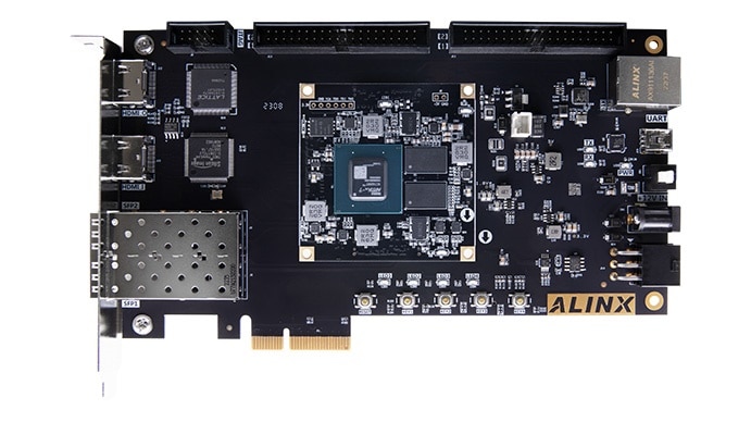
Each time I start s new version I end up upgrading the FPGA cards used. This time I have updated to an Alinx AXKU3: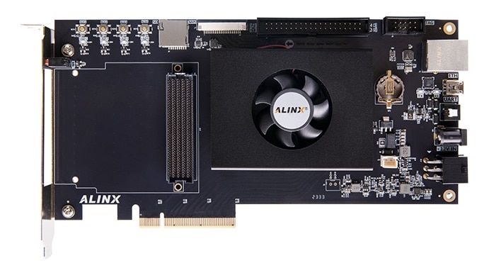
This card is used to connect to 1 thru 4 ADC sample cards via 8GB fiber.
=======================================================================================
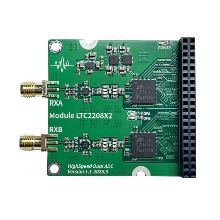
I am refitting the previously used Alinx XC7K325 to simulate 4 separate ADC cards, each with an ADC running at 60.44MHZ/122.88MHz
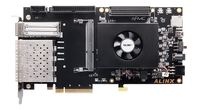
The real system will have 3-4 cards, each with 1 ADC.
=============================================================================================
The sample transfer math (sample rate x 2 bytes per sample x 8 bits per byte x 4 ADCs)
4 2217s sampled at 61.440MHz (DC thru 10 meters) gives us: 61,440,000 × 2 × 8 × 4 = 3,932,160,000 bits per second
4 2208s sampled at 122.880MHz (DC thru 6 meters) gives us: 122,880,000 × 2 × 8 × 4 = 7,864,320,000 bits per second.
To achieve this xfer speed, without loosing any data I had to:
- Go to a faster CPU (threadripper)
- enable Ubuntu low latency features
================================================================================================
The main CPU box uses an c Asus
It has an MSI Gaming RTX 5070 Ti for processing ADC samples:

And a VisionTek 550 for video display:
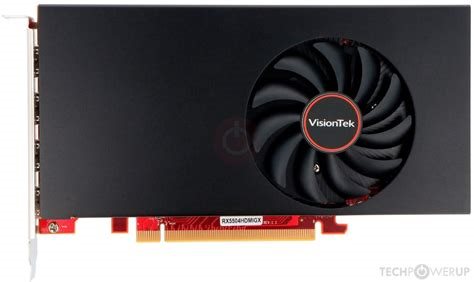
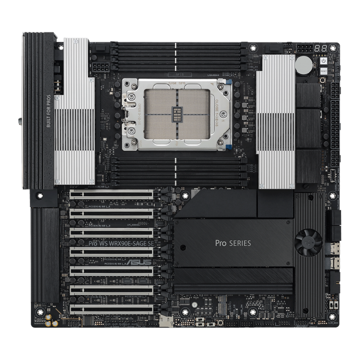
It all sits in an Asus ASUS Pro WS WRX90E-SAGE SE EEB Workstation Motherboard:
It all sits in a large case:

=============================================================================
Getting all that hardware up and happy was a pain. This site got me thru it:
It seems like overkill, but the Ripper makes Vivado builds faster, the GPU provides processing power for the ADC samples, the VisionTek keeps
display duties separate from the GPU.
=================================================================================================================
The kernel drivers are on github:
https://github.com/Xilinx/dma_ip_drivers
=================================================================================================================
I'm using Vivado 2023.2 for FPGA design. It has a simple licensing scheme:
https://www.amd.com/en/support/downloads/adaptive-socs-and-fpgas/development-tools/2023-2.html
I installed this:

The latest is 2026.x:
Xilinx made major changes to the license between the two. Read the info carefully before making a decision!
Check with your vendor to see if they offer a license voucher for the board you are considering, it can save you bug buck$
https://adaptivesupport.amd.com/s/article/43853?language=en_US
=================================================================================================================
===================================================================================================================
I was looking around for info on real-time linux when I discovered Ubuntu already had low-latency features built in, They just need ed to be turned on:
I used audio: preempt=full nohz_full=all threadirqs:
# https://discourse.ubuntu.com/t/fine-tuning-the-ubuntu-24-04-kernel-for-low-latency-throughput-and-power-efficiency/44834
#GRUB_CMDLINE_LINUX_DEFAULT="quiet splash"
GRUB_CMDLINE_LINUX_DEFAULT="quiet splash preempt=full nohz_full=all threadirqs isolcpus=30-31"
Simply copy paste the options above for the desired performance profile and add them to the GRUB_CMDLINE_LINUX_DEFAULT= line in /etc/default/grub
(then run sudo update-grub to apply them at the next reboot).
Note that I also isolated cpus 30 and 31 for exclusive use with the test program.
You can test changes by running this line after boot:
$ sudo dmesg | grep "Command line"

[  0.000000] Command line: BOOT_IMAGE=/boot/vmlinuz-7.0.0-30-generic root=UUID=773717ed-b1a9-4b11-8fbb-7dd21ff67abb ro quiet splash preempt=full nohz_full=all threadirqs isolcpus=30-31 vt.handoff=7
$ grep -E "CONFIG_*" /boot/config-$(uname -r)

...

CONFIG_NO_HZ_FULL=y

...

CONFIG_RCU_NOCB_CPU=y

...

CONFIG_PREEMPT_BUILD=y

CONFIG_ARCH_HAS_PREEMPT_LAZY=y

# CONFIG_PREEMPT is not set

CONFIG_PREEMPT_LAZY=y

# CONFIG_PREEMPT_RT is not set

CONFIG_PREEMPT_COUNT=y

CONFIG_PREEMPTION=y

CONFIG_PREEMPT_DYNAMIC=y
===================================================================================================================
These changes alone made it possible to read samples for an hour or so before loosing data. But I need days, so quest is on to use Xilinx Virtual Fifo IP:
https://docs.amd.com/v/u/en-US/pg038_axi_vfifo_ctrl

I tried using traditional BRAM fifos but ran out of available BRAM. The DMA read is of 65536 bytes, which is quickly overruns the read buffer.
By using the virtual FIFO with DDR4 backing ram I get very large buffers.
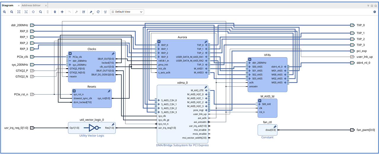
The complete fifoBrd design:
=====================================
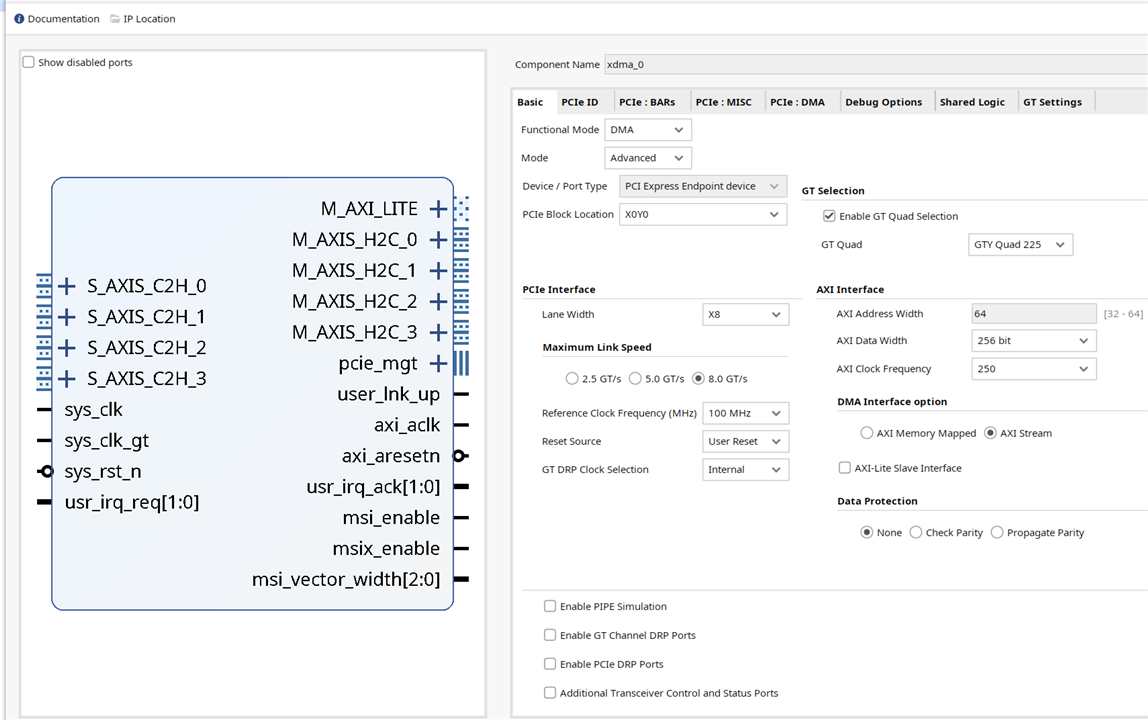
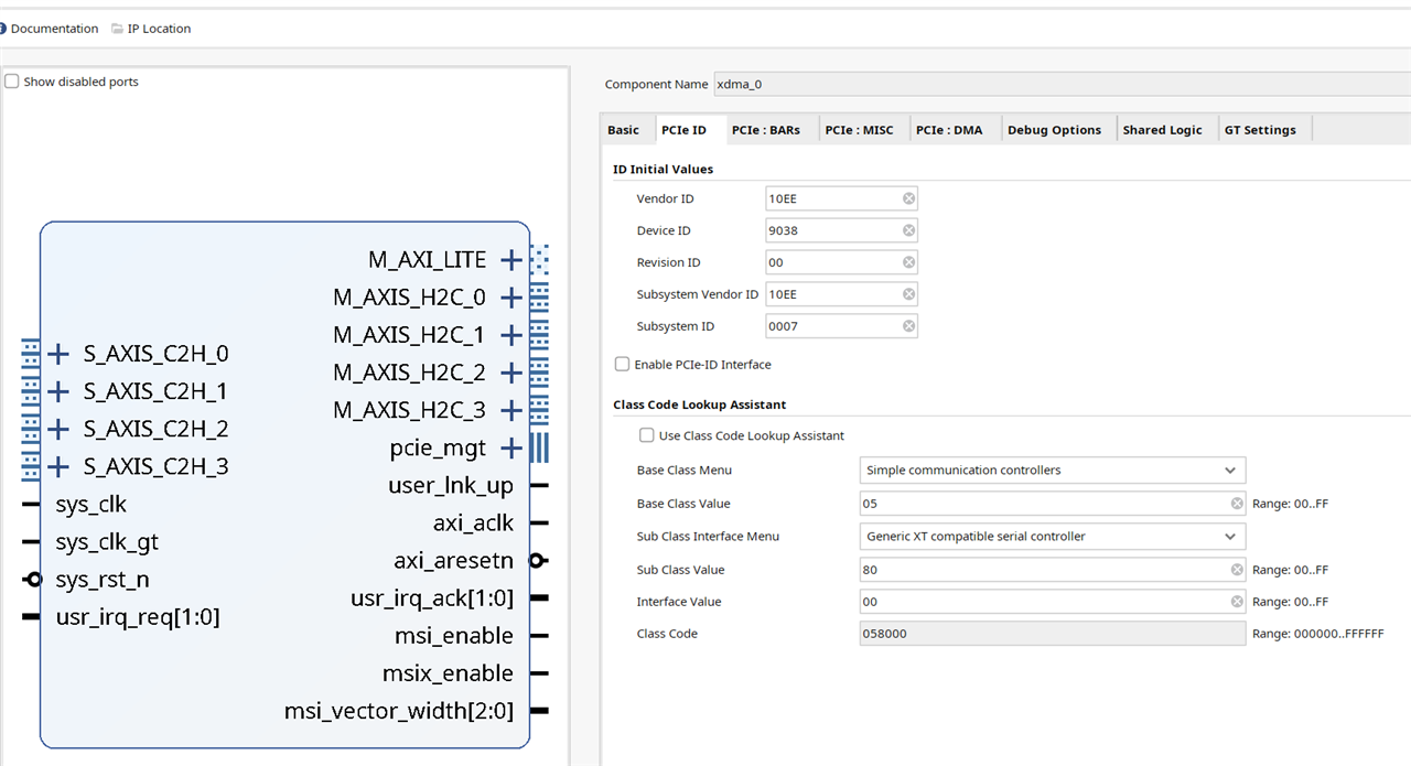
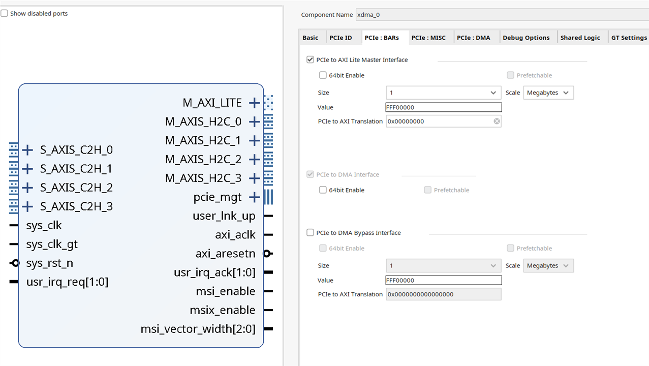
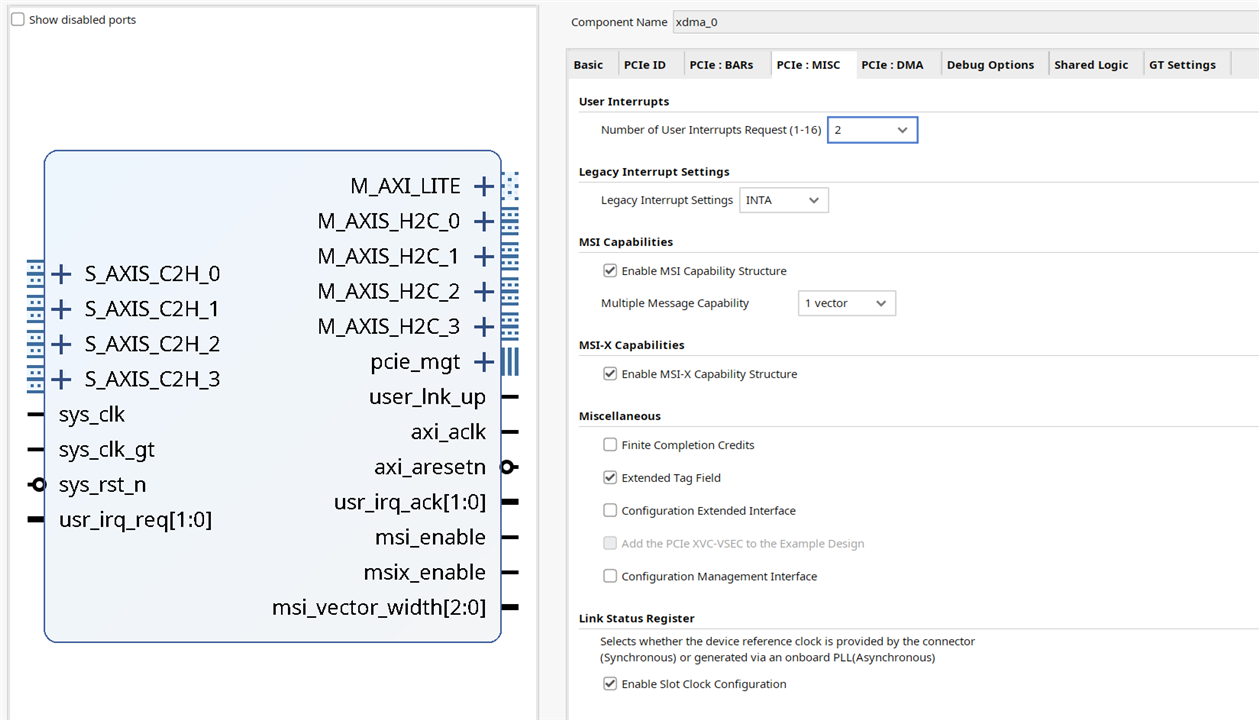
XDMA Configuration:
Basic:
PCIe ID:
PCIe Bars:
PCIe Misc:
PCIe DMA:
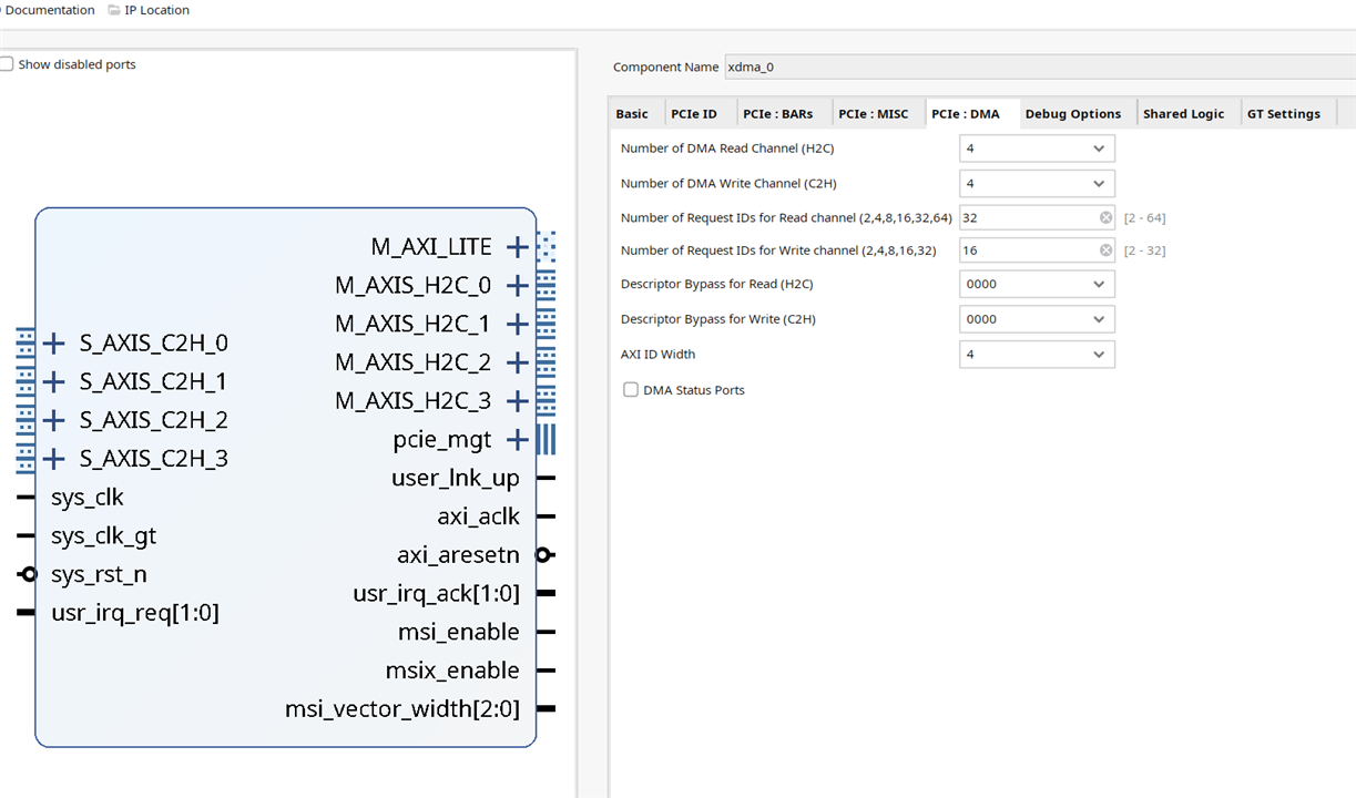
Shared Logic:
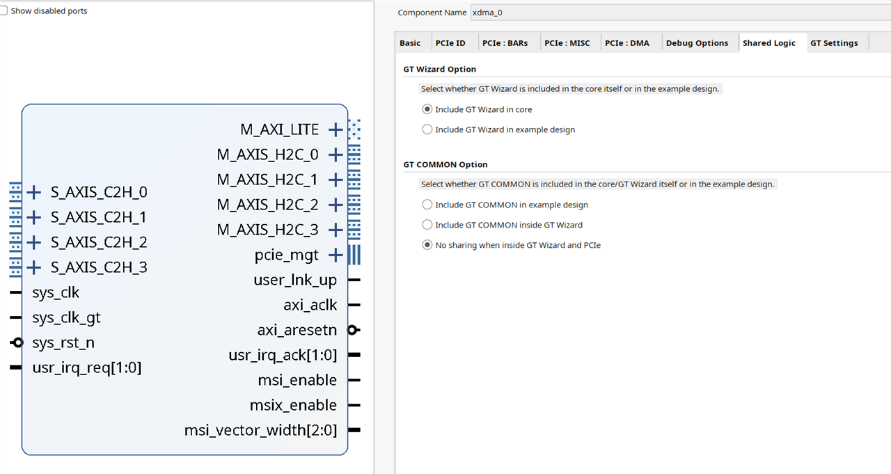
GT Settings:
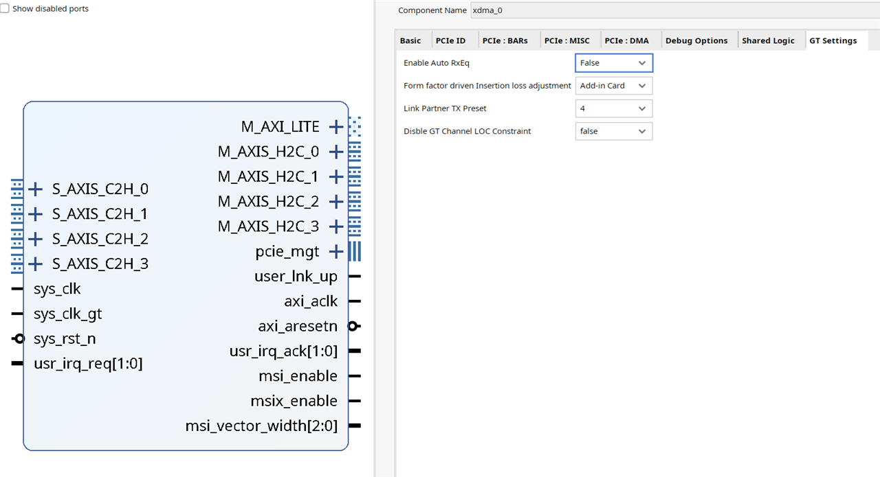
=====================================
There are 4 fiber channels built with Aurora IP:
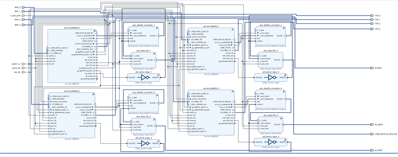
Aurora Configuration:
Core Options:
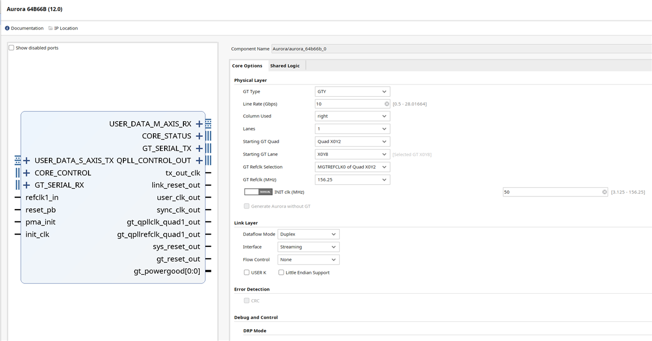
Note the Starting GT Lane box, set to X0Y8. Each aurora uses a different GT lane: X0Y8, X0Y9, X0Y10 and X0Y11. Other settings are common between the 4 aurora.
Shared Logic:
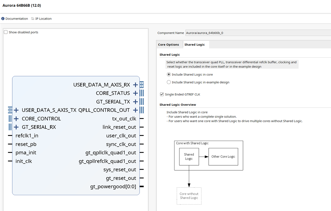
The proper settings for Starting Quad etc. will depend on the FPGA and board design. Most board manufacturers
will offer a set of demo designs along with tutorials in their use. Be sure to verify this before you purchase.
Look for a sample PCIe (ie. XDMA IP) as well as a design using Aurora. I have 4 or 5 Alinx boards, and the demos
are fairly extensive. Not always completely translated to English, google translate is your friend.
=====================================
The block has 4 Aurora IP, one per channel. Each channel has an Aurora, a dwidth converter and a small fifo:
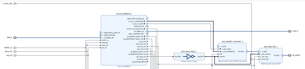
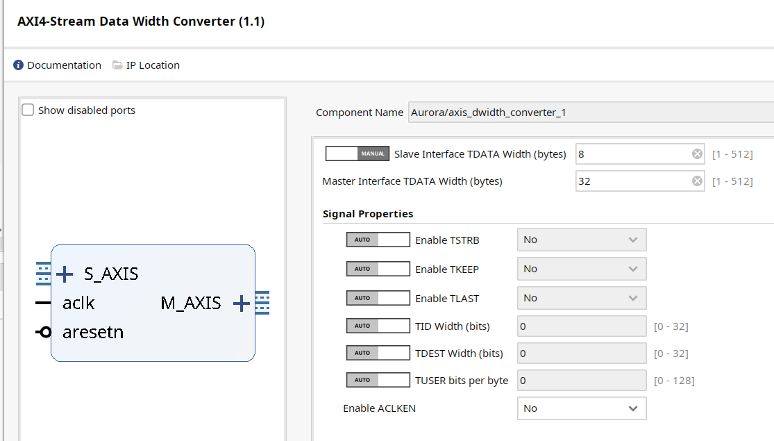
The dwidth converter ised to convert the 8 byte wide aurora stream to a 32 byte wide stream:
=====================================
DWidth Converter Configuration:
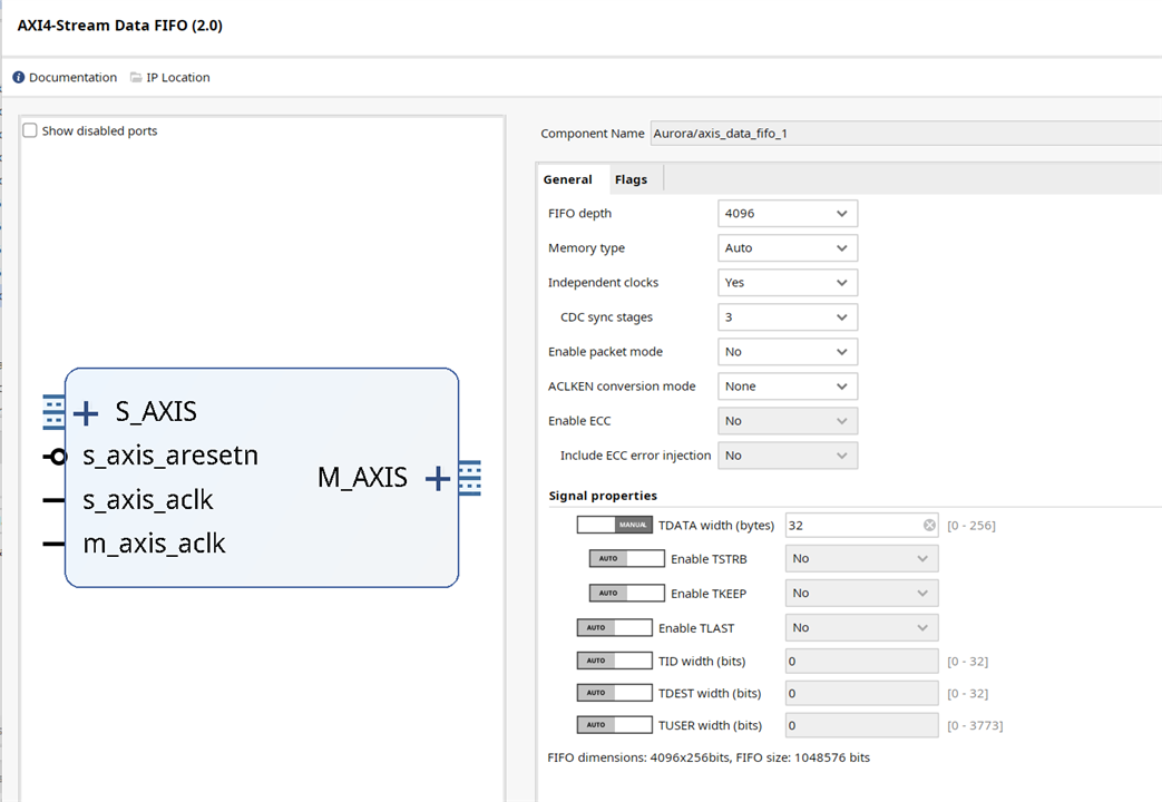
The Stream fifo is used to buffer the data and to change transfer speeds. Note that the Independent clocks box is checked.
The creates a wire for s_axis_aclk and m_axis_aclk, allowing it to xfer data from aurora at its native 156.25MHz rate and on
to M_AXIS at 250MHz, which is the clock speed of the axis switch it feeds:
=====================================
AXIS Data Fifo Configuration:
=====================================
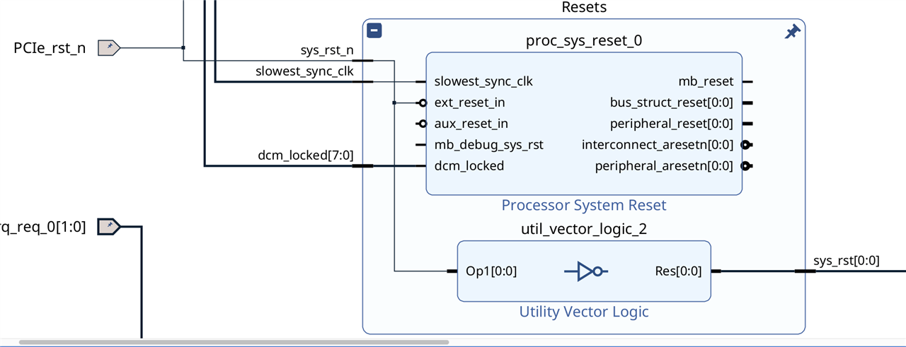
The reset circuit:
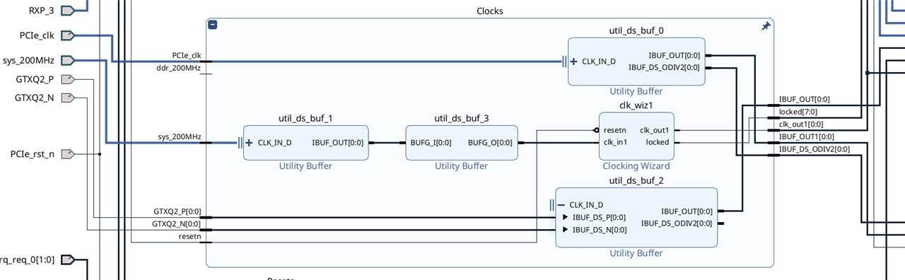
And the clock circuits:
==================================================================================================
I spent WEEKS trying to make it work without luck.
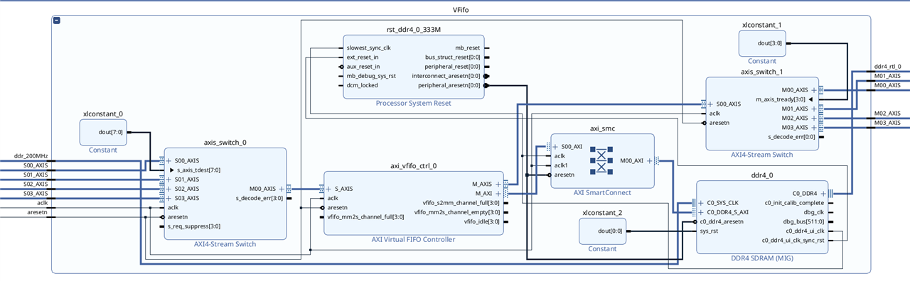
Googled more sites than I thought existed. Almost all concluded that vfifo didn't really work... The secret is the design of the 2 switches
The board design of the vfifo looks like:
The input switch:

I had assumed that if you send data into S00_AXIS it would magically come out of the 2nd switch on M00_AXIS.
Not so, you have to explicitly set the TDEST for each channel when used. In our design there is no need for dynamic switching, so we set the paths with a CONST:
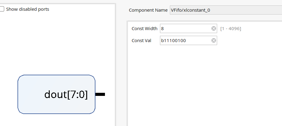
Note the binary value of 11 10 01 00. This causes a TDEST value of 00 to be added to S00_AXIS, 01 to S01_AXIS, etc. It is configured as:
=====================================
Switch 0 Configuration:
Switch Properties:
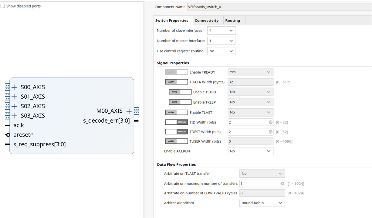
Connectivity:

Routing:

=====================================
Switch 1 Configuration:
Switch Properties:
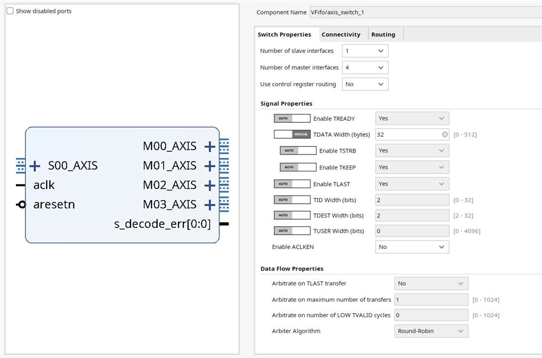
Connectivity:
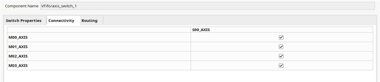
Routing:

=====================================
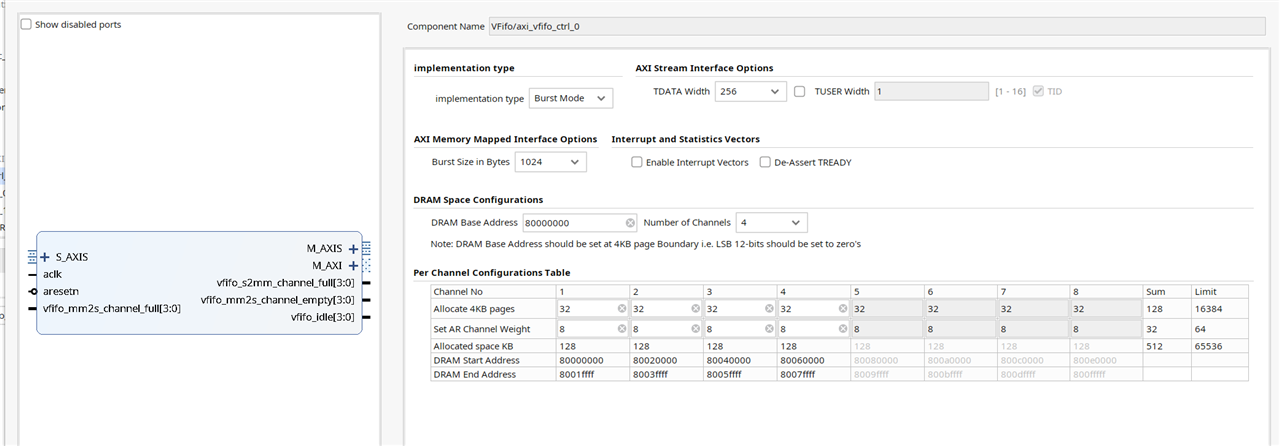
Virtual FIFO Configuration:
=====================================
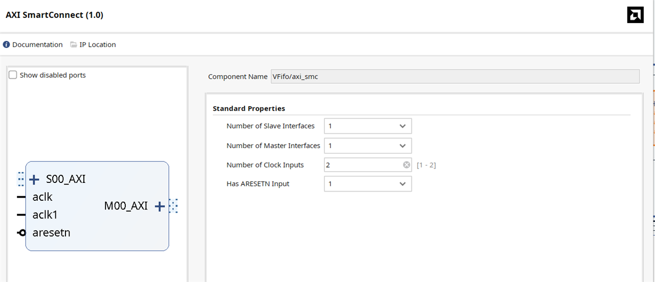
Smart Connect Configuration:
Standard Properties:
=====================================
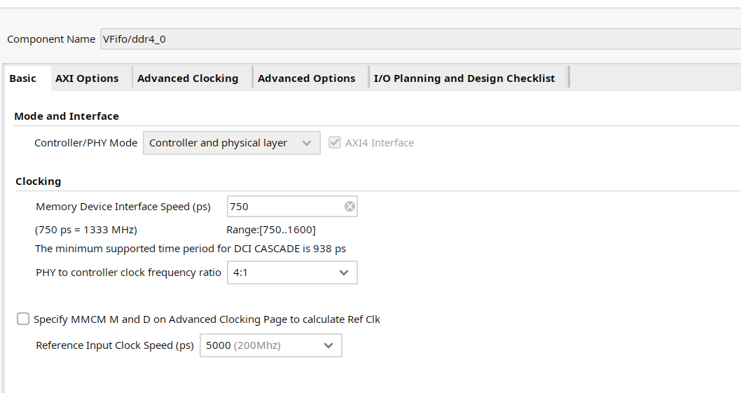
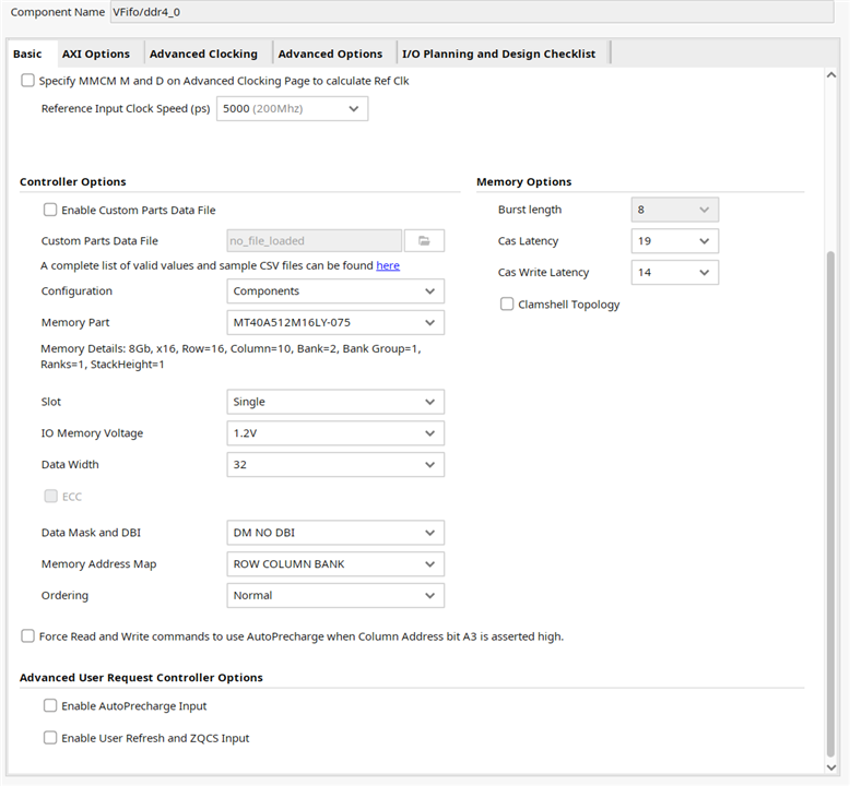
DDR4 MIG Configuration:
Basic part 1:
Basic part 2:
AXI Options:
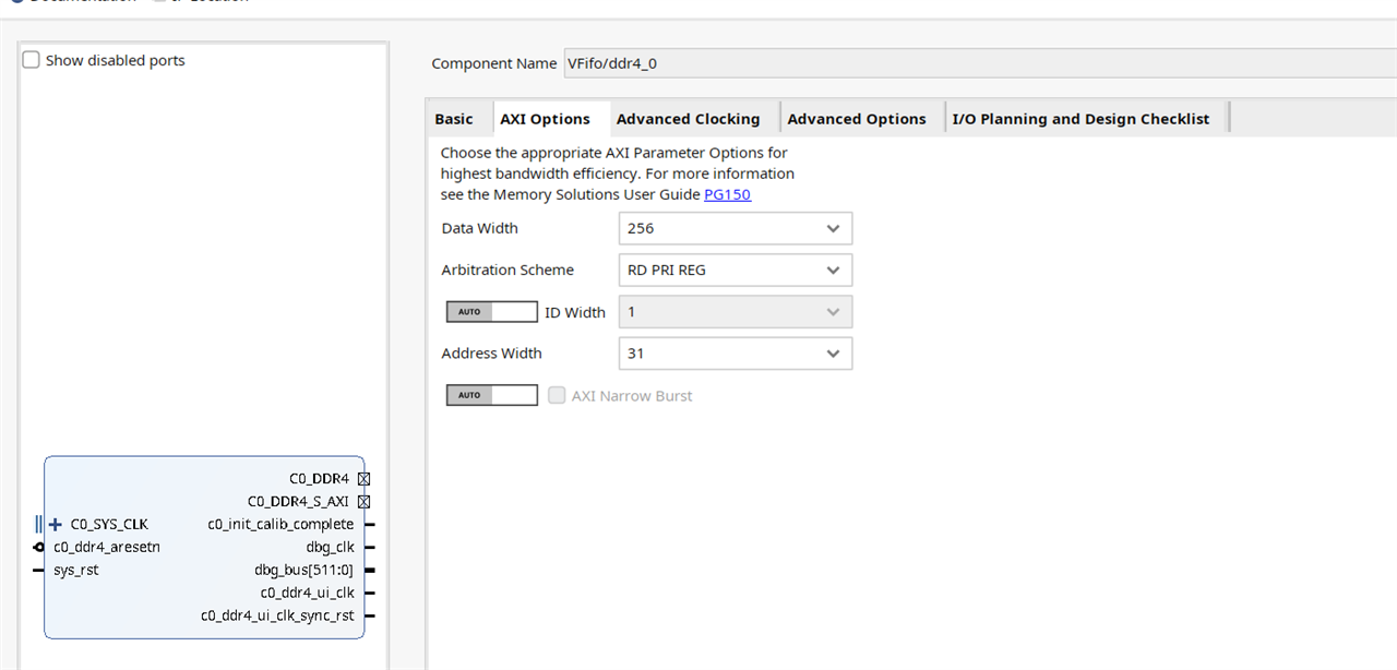
Advanced Clocking:
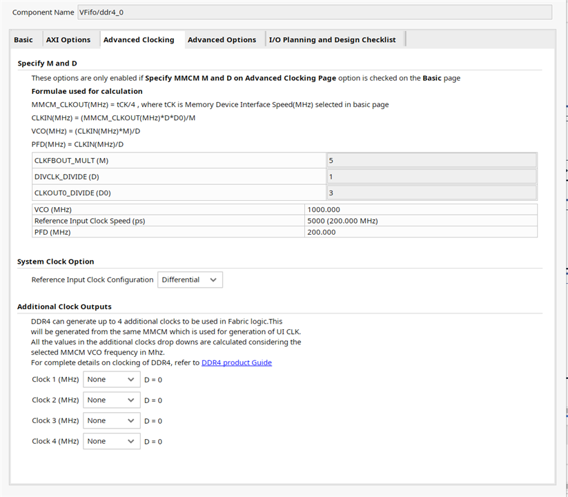
Advanced Options:
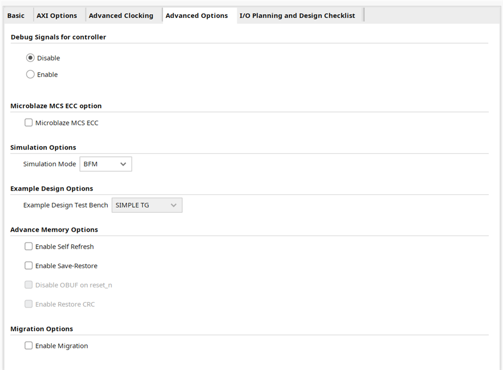
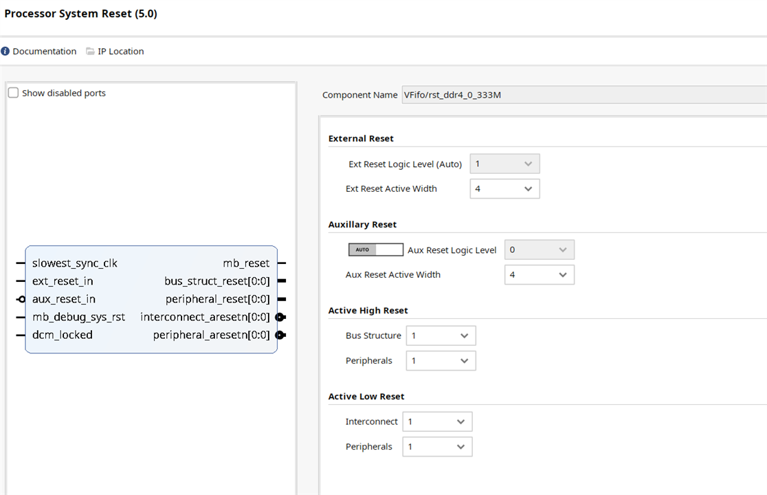
=====================================
Processor System Reset:
=====================================
wrAXI4Lite:
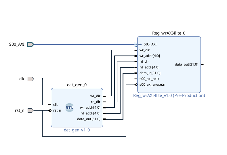
I use the above IP to generate an ID string:
$ sudo getid
AUXK3 fifoBrd4x Fri Sep 18 11:25:50 2026
The RTL:
`timescale 1ns / 1ps
//////////////////////////////////////////////////////////////////////////////////
// Company:
// Engineer:
//
// Create Date: 2018/11/16 15:11:13
// Design Name:
// Module Name: dat_gen
// Project Name:
// Target Devices:
// Tool Versions:
// Description:
//
// Dependencies:
//
// Revision:
// Revision 0.01 - File Created
// Additional Comments:
//
//////////////////////////////////////////////////////////////////////////////////


module dat_gen(
	       input		 clk,
	       input		 rst_n,
	       output reg	 wr_dir,
	       output reg	 rd_dir,
	       output reg [4:0]	 wr_addr,
	       output reg [4:0]	 rd_addr,
	       output reg [31:0] data_out
);

 always @( posedge clk or negedge rst_n)
    begin
    if ( rst_n == 1'b0 )
	begin
	wr_dir  <=1'b0;
	rd_dir  <=1'b0;
	end
    else
	begin
	wr_dir  <=1'b1;
	rd_dir  <=1'b1;
	end
  end

   always @( *)
     begin
	if( wr_dir)
	  begin
	     case (wr_addr)
// AUXK3 fifoBrdX4 Sat Sep  5 21:39:29 2026
	      5'h00   : data_out     <= 32'h4b58_5541;  // AUXK
	      5'h01   : data_out     <= 32'h6966_2033;  // 3 fi
	      5'h02   : data_out     <= 32'h7242_6f66;  // foBr
	      5'h03   : data_out     <= 32'h2034_5864;  // dX4
	      5'h04   : data_out     <= 32'h2074_6153;  // Sat
	      5'h05   : data_out     <= 32'h2070_6553;  // Sep
	      5'h06   : data_out     <= 32'h3220_3520;  //  5 2
	      5'h07   : data_out     <= 32'h3933_3a31;  // 1:39
	      5'h08   : data_out     <= 32'h2039_323a;  // :29
	      5'h09   : data_out     <= 32'h3632_3032;  // 2026
	      5'h0a   : data_out     <= 32'h0000_0000;  //
	      5'h0b   : data_out     <= 32'h0000_0000;  //
	       default : data_out     <=data_out ;
	     endcase
	  end
     end


   always @( posedge clk or negedge rst_n)
     begin
	if ( rst_n == 1'b0 )
	  begin
	     rd_addr         <=5'd12;
	  end
	else
	  begin
	     rd_addr         <=5'd12;
	  end
     end

   always @( posedge clk or negedge rst_n)
     begin
	if ( rst_n == 1'b0 )
	  begin
	     wr_addr         <=5'd0;
	  end
	else if(wr_dir)
	  begin
	     if(wr_addr==9)
	       wr_addr         <=5'd0;
	     else wr_addr         <=wr_addr+1'b1;
	  end
     end
endmodule
====================================
This is where it gets tricky:
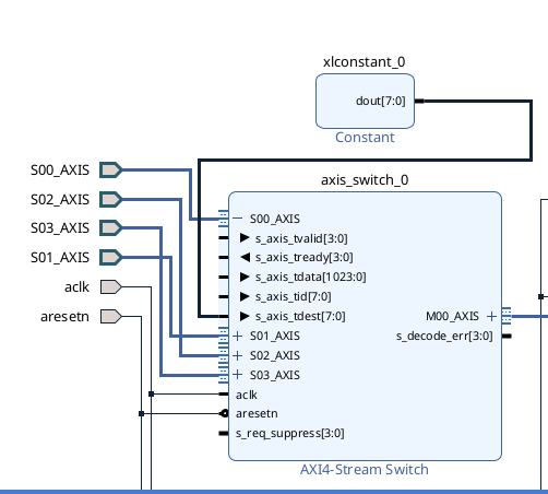
To be able to connect the wire you have to expand S00_AXIS and attach to tdest[7:0] This is actually the 4 sets of 2 bit destinations. You only need to do this with S00_AXIS
It attaches 2 bits to each of S0n_AXIS.
A similar issue exists with switch 1:
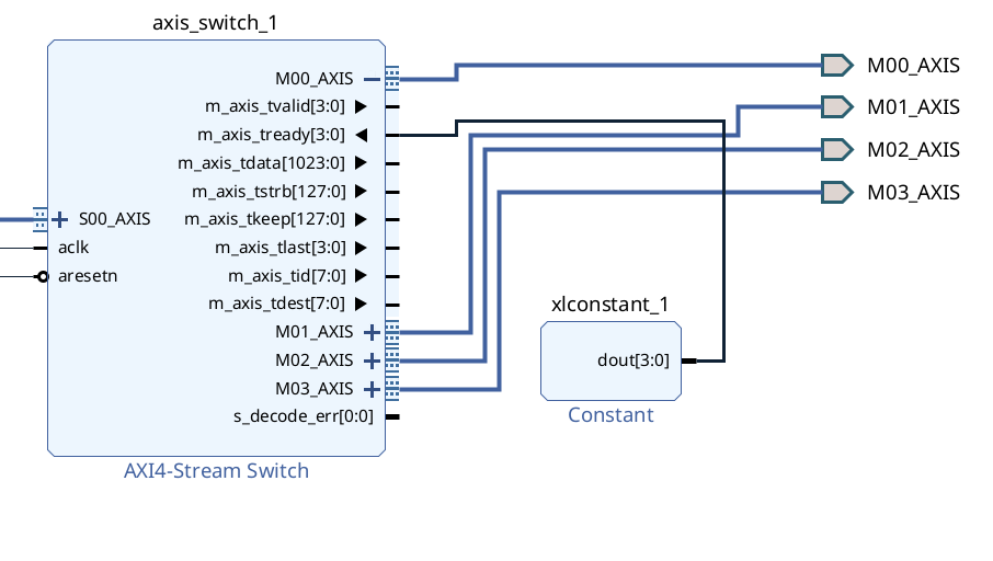
Here the CONST should be b'1111 Don't know how to explain, but it causes data from S00_AXIS to travel thru M00_AXIS, etc. Again, only necessary to wire M00_AXIS.
It attaches 1 bit to each of M0n_AXIS.
=======================================================================================================
The ADC simulation board:
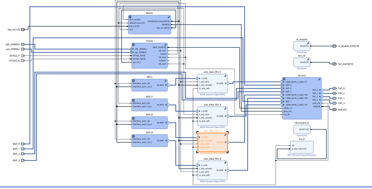
Each channel:
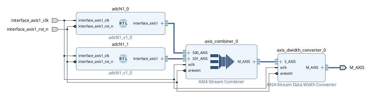
This is 2 virtual ADCs, each clocked at 61.44MHz:
//===========================================================================
// Module name: adcN1.v
//===========================================================================

`timescale 1ns / 1ps
module adcN1
(
 interface_axis1_clk,
 interface_axis1_rst_n,

 interface_axis1_tdata,
 interface_axis1_tready,
 interface_axis1_tvalid,
);

//===========================================================================
// PORT declarations
//===========================================================================
   input           interface_axis1_clk;
   input           interface_axis1_rst_n;

   input           interface_axis1_tready;

   output          interface_axis1_tdata;
   output          interface_axis1_tvalid;

   reg [15:0]      interface_axis1_tdata;
   reg             interface_axis1_tvalid;

//===========================================================================
//
//===========================================================================
always @(posedge interface_axis1_clk or negedge interface_axis1_rst_n)
begin
  if (~interface_axis1_rst_n)
    begin
       interface_axis1_tvalid = 1'b1;
       interface_axis1_tdata = 16'h0000;
    end
  else
    begin
       interface_axis1_tdata <= interface_axis1_tdata + 1;
    end
end
This creates a stream of 16 bit sample pairs, each spanning 0x0000 thru 0xffff. Bottom line is each of four channels producing equivalent of 1 ADC clocked at 122.88MHz.
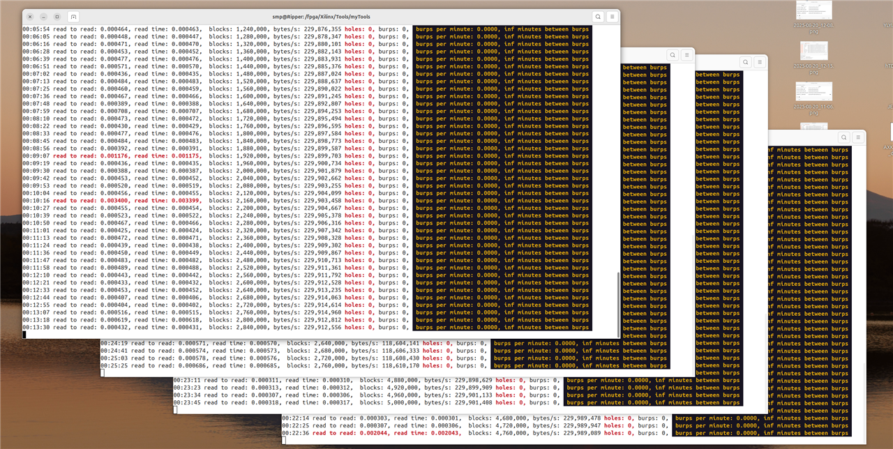
This pattern can be examined on the main board for any gaps or bad data.
$ sudo ./fifotest
>>> xdma device: c2h_0
95509550 95519551 95529552 95539553 95549554 95559555 95569556 95579557 95589558 95599559 955a955a 955b955b 1e141e14 1e151e15 1e161e16 1e171e17
1e181e18 1e191e19 1e1a1e1a 1e1b1e1b 1e1c1e1c 1e1d1e1d 1e1e1e1e 1e1f1e1f 1e201e20 1e211e21 1e221e22 1e231e23 1e241e24 1e251e25 1e261e26 1e271e27
1e281e28 1e291e29 1e2a1e2a 1e2b1e2b 1e2c1e2c 1e2d1e2d 1e2e1e2e 1e2f1e2f 1e301e30 1e311e31 1e321e32 1e331e33 1e341e34 1e351e35 1e361e36 1e371e37
1e381e38 1e391e39 1e3a1e3a 1e3b1e3b 1e3c1e3c 1e3d1e3d 1e3e1e3e 1e3f1e3f 1e401e40 1e411e41 1e421e42 1e431e43 1e441e44 1e451e45 1e461e46 1e471e47
1e481e48 1e491e49 1e4a1e4a 1e4b1e4b 1e4c1e4c 1e4d1e4d 1e4e1e4e 1e4f1e4f 1e501e50 1e511e51 1e521e52 1e531e53 1e541e54 1e551e55 1e561e56 1e571e57
1e581e58 1e591e59 1e5a1e5a 1e5b1e5b 1e5c1e5c 1e5d1e5d 1e5e1e5e 1e5f1e5f 1e601e60 1e611e61 1e621e62 1e631e63 1e641e64 1e651e65 1e661e66 1e671e67
Note how this creates a repeating pair of identical samples. These can be examined after xfer and corruption can be found. The test itself is a pthreaded program with 2 threads,
a reader:
    while (1) {
        pWait(&readBufferEmpty[pong]);
        amount = read(h, (void*)read_data[pong], (size_t)dma_block_size);
        pSignal(&readBufferFull[pong]);
        pong = pong ? 0 : 1;
     }
      ...
, and a checker:
next:
    pWait(&readBufferFull[ping]);
       /// various tests of pattern...
    pSignal(&readBufferEmpty[ping]);
      ping = ping ? 0 : 1;
      goto next;
In the real program the checker is replaced by a routine to pass the data on to the GPU card for processing. 4 copies of the test, running on each of the 4 channels:
==============================================================================================================
=====================================
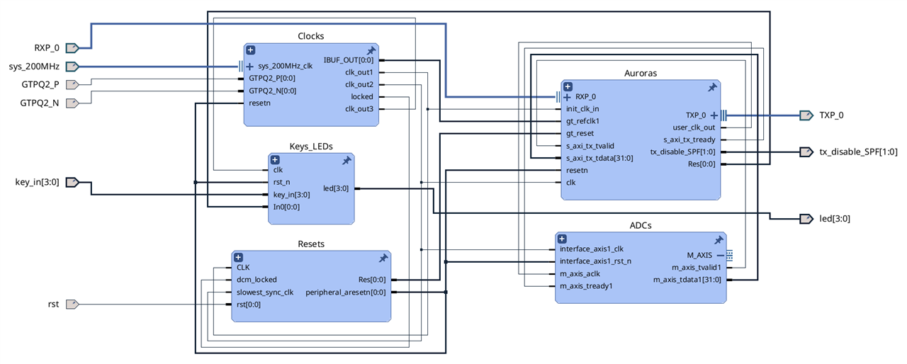
Chapter II:
a