


I received the Digilent Arty S7 50 Board for the 7 Ways to Leave Your Spartan-6 FPGA program. In this blog I describe what the first power up of the board is like and then a small tutorial on how to create your first Hardware-Only design.
First Power Up
For more info about the board refer to Arty S7 - Digilent Reference
As soon as you plug in the board, a pre-installed bitstream runs. My board has a problem and it only works with usb power, there must be some component damaged and the AD2384 voltage regulator has burned out, see discussion: Arty S7 rev B vs Arty S7 rev E? Somewhat confused. - Forum - FPGA - element14 Community

On the back of the board you can see which board revision it is, necessary to be able to check the updated schematic. My board is Revision B
https://digilent.com/reference/_media/reference/programmable-logic/arty-s7/arty_s7_sch-rev_b.pdf

The board comes with a bitstream preloaded. You can play with the switches and buttons.
Hardware-Only Blinky Counter Tutorial
This tutorial is based on Getting Started with Vivado for Hardware-Only Designs - Digilent Reference
Install Vivado. I'm using Vivado ML Editions 2021.1 for this demo. I have a very slow ADSL Internet connection and I had Vivado previously installed with that version.
Open Vivado and Create Project

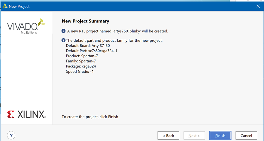
Create project

Select default part

Review Project Summary
From Arty S7 - Digilent Reference go to Master XDC Files Repository

Download Master XDC files as zip or go to digilent-xdc/Arty-S7-50-Master.xdc at master · Digilent/digilent-xdc · GitHub and copy the lines you need.

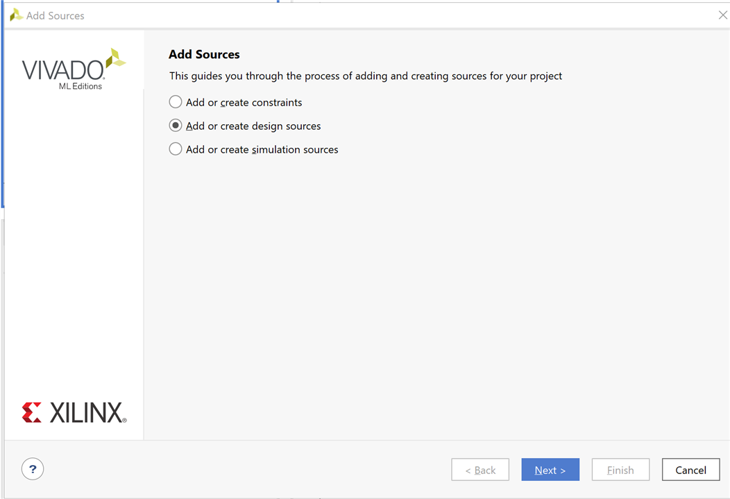
From Vivado Sources right click over constraints and click on add sources


You can add the Arty-S7-50-Master.xdc file downloaded from github, then uncomment the lines corresponding to used pins and rename the used ports (in each line, after get_ports) according to the top level signal names in the project or create a new constraints file and edit your configuration.
For clarity I created a new file artys7_50.xdc

Edit the new file and copy and rename the ports

Configure one clock signal as clk, one switch button as sw and four leds led[0..3]
## Clock Signals
set_property -dict { PACKAGE_PIN F14   IOSTANDARD LVCMOS33 } [get_ports { clk }]; #IO_L13P_T2_MRCC_15 Sch=uclk
create_clock -add -name sys_clk_pin -period 83.333 -waveform {0 41.667} [get_ports { clk }];

## Switches
set_property -dict { PACKAGE_PIN H14   IOSTANDARD LVCMOS33 } [get_ports { sw }]; #IO_L20N_T3_A19_15 Sch=sw[0]

## LEDs
set_property -dict { PACKAGE_PIN E18   IOSTANDARD LVCMOS33 } [get_ports { led[0] }]; #IO_L16N_T2_A27_15 Sch=led[2]
set_property -dict { PACKAGE_PIN F13   IOSTANDARD LVCMOS33 } [get_ports { led[1] }]; #IO_L17P_T2_A26_15 Sch=led[3]
set_property -dict { PACKAGE_PIN E13   IOSTANDARD LVCMOS33 } [get_ports { led[2] }]; #IO_L17N_T2_A25_15 Sch=led[4]
set_property -dict { PACKAGE_PIN H15   IOSTANDARD LVCMOS33 } [get_ports { led[3] }]; #IO_L18P_T2_A24_15 Sch=led[5]


##Configuration options, can be used for all designs
set_property BITSTREAM.CONFIG.CONFIGRATE 50 [current_design]
set_property CONFIG_VOLTAGE 3.3 [current_design]
set_property CFGBVS VCCO [current_design]
set_property BITSTREAM.CONFIG.SPI_BUSWIDTH 4 [current_design]
set_property CONFIG_MODE SPIx4 [current_design]

# SW3 is assigned to a pin M5 in the 1.35v bank. This pin can also be used as
# the VREF for BANK 34. To be able to use this pin as an ordinary I/O the
# following property must be set to enable an internal VREF for BANK 34.
# Since a 1.35v supply is being used the internal reference is set to half that
# value (i.e. 0.675v).
#
set_property INTERNAL_VREF 0.675 [get_iobanks 34]

set_property BITSTREAM.GENERAL.COMPRESS TRUE [current_design]
Create a design source. Again right click over Design Sources and Add Sources, now Add or create design sources
Create Source File. Select your preferred Hardware Design Language, HDL. I selected Verilog
And name your file. File location is ok by default.

Press ok and finish adding sources
After clicking finish you are asked to define the new Module
Use the same name ports as in your constraints file: clk, sw and led. led is a bus with 4 lines

- Port Name: This field defines the name of the port and needs to match one of the names you used in your XDC file.
- Direction: This drop-down menu can be set to input, output, or inout, defining the direction that signals propagate through this port, with respect to your module. Outputs are the signals that your module will be controlling.
- Bus: This can be checked or not, when checked, this port consists of multiple single bit signals, grouped into a single bus.
- MSB: The index of the most significant bit of the port, if it is a bus. This option is grayed out for single-bit ports.
- LSB: The index of the least significant bit of the port, if it is a bus. This option is grayed out for single-bit ports.
Click OK and now you can edit blinky4.v module

`timescale 1ns / 1ps

module blinky4(
    input clk,
    output [0:3] led,
    input sw
    );
// reg for counter
reg [24:0] count = 0;

assign led[0] = count[21];
assign led[1] = count[22];
assign led[2] = count[23];
assign led[3] = count[24];

always @ (posedge(clk)) count <= count + 1;
endmodule
Save and run synthesis
After synthesis is completed you'll get a dialog

Click OK for running Implementation
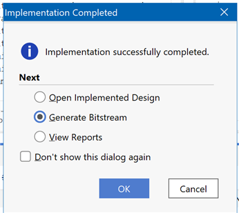
When Implementation is completed you're asked again for the next action. Now we select Generate Bitstream
Connect your Arty S7 50 board to your PC
Open Hardware Manager

or


Then program device uploading the new bitstream


You're done. Your blinky counter running:

