For the 7 Ways to Leave Your Spartan-6 program I am writing a series of tutorials to explore the possibilities of the Arty S7 50 board. In the first tutorial we explored creating hardware-only projects without using pre-built IPs. In this tutorial we go one step further and configure our FPGA as a RISC microcontroller.
The Arty S7 is very flexible thanks to its FPGA. We can transform an FPGA into a custom software-defined system on a chip (SoC). Using the Vivado IP Integrator (Vivado IPI) graphical tool, we can easily make FPGA “Soft SoC” configurations.
Vivado IPI allows us to select pre-built IP blocks like timers, UART/SPI/IIC controllers and many of the other devices you would normally find in a SoC or microcontroller.
In this tutorial we will use AMD Xilinx Vivado to configure our FPGA hardware and AMD Xilinx Vitis to program the MicroBlaze soft processor in C language.
For this tutorial I followed this guide: Getting Started with Vivado and Vitis for Baremetal Software Projects - Digilent Reference
In the following video you can see the final result of the project, a simple baremetal program executed on a MicroBlaze soft processor that allows you to turn on 4 LEDs with four buttons, one assigned to each LED and sends text through the configured UART port when it starts.
Introduction to the MicroBlaze soft processor
The MicroBlaze embedded processor soft core is a reduced instruction set computer (RISC) optimized for implementation in Xilinx® Field Programmable Gate Arrays (FPGAs).
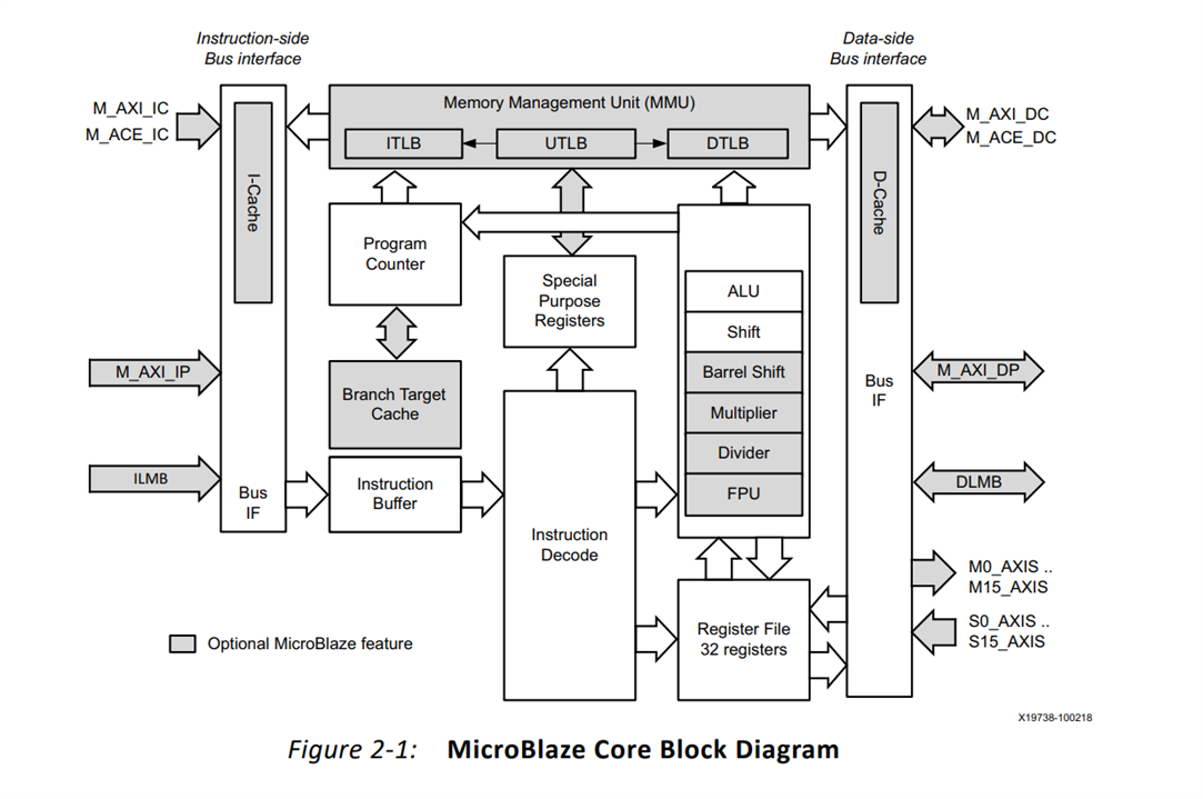
MicroBlaze is the Xilinx FPGA-based, 32-bit/64-bit RISC Harvard architecture soft processor. It supports advanced architecture options such as AXI interface, Memory Management Unit (MMU), instruction and data-side cache, configurable pipeline depth and Floating-Point Unit (FPU).
The following figure shows a functional block diagram of the MicroBlaze core.
References:
- ug984-vivado-microblaze-ref.pdf • Viewer • Documentation Portal (xilinx.com)
- MicroBlaze Processor Quick Start Guide for Vitis 2021.1 (xilinx.com)
The MicroBlaze processor is commonly used in one of three preset configurations listed below:
- A simple microcontroller running bare-metal applications
- A real-time processor featuring cache and a memory protection unit interfacing to tightly coupled on-chip memory, running FreeRTOS
- An application processor with a memory management unit running Linux
In this tutorial we will not use the preset configurations. We are going to make a simple bare metal application with hardware consisting of a MicroBlaze soft processor, 1 DDR3 SDRAM module, 4 buttons, 4 LEDs and a UART interface.
Tutorial environment
For this project tutorial I used
- AMD Xilinx Vivado 2021.1,
- AMD Xilinx Vitis 2021.1,
- Digilent Arty S7 50
- Windows 10
Hardware Development
Hardware Project creation
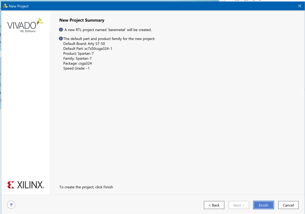
First we are going to create a new Vivado project to configure our FPGA as a MicroBlaze soft processor with some specific inputs and outputs.
Create a Vivado Project: see my firs blog Arty S7 50 First Power Up and Hardware-Only Blinky - Blog - FPGA - element14 Community
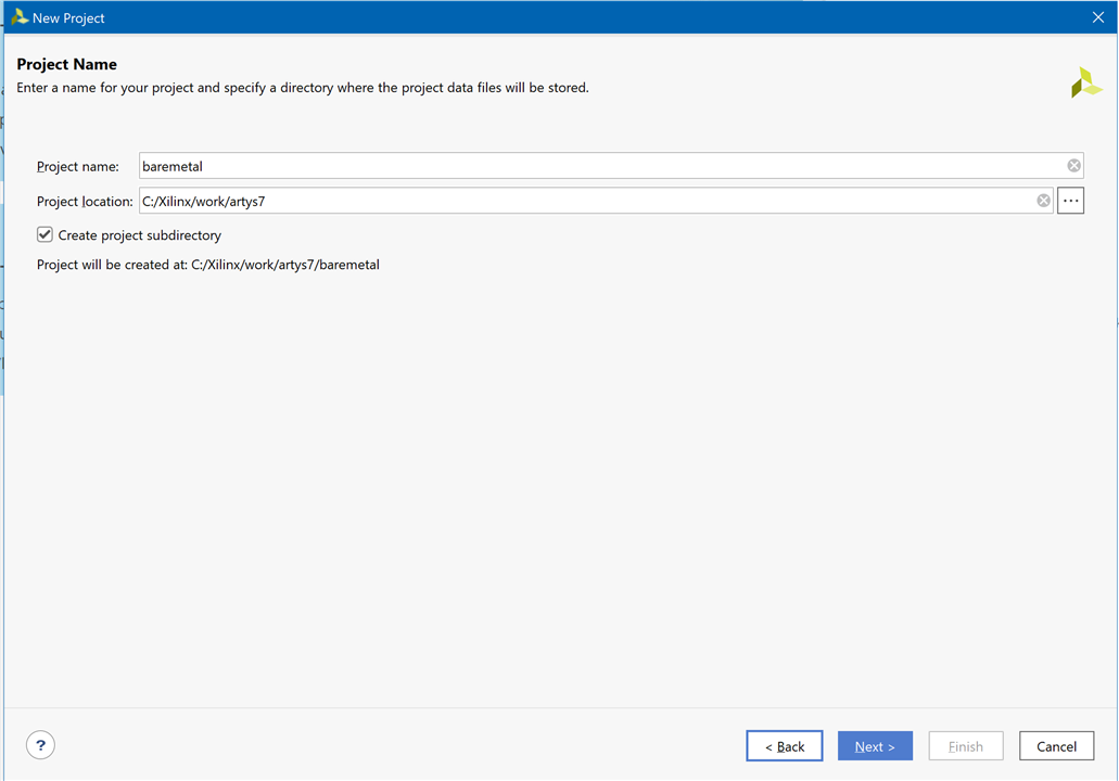
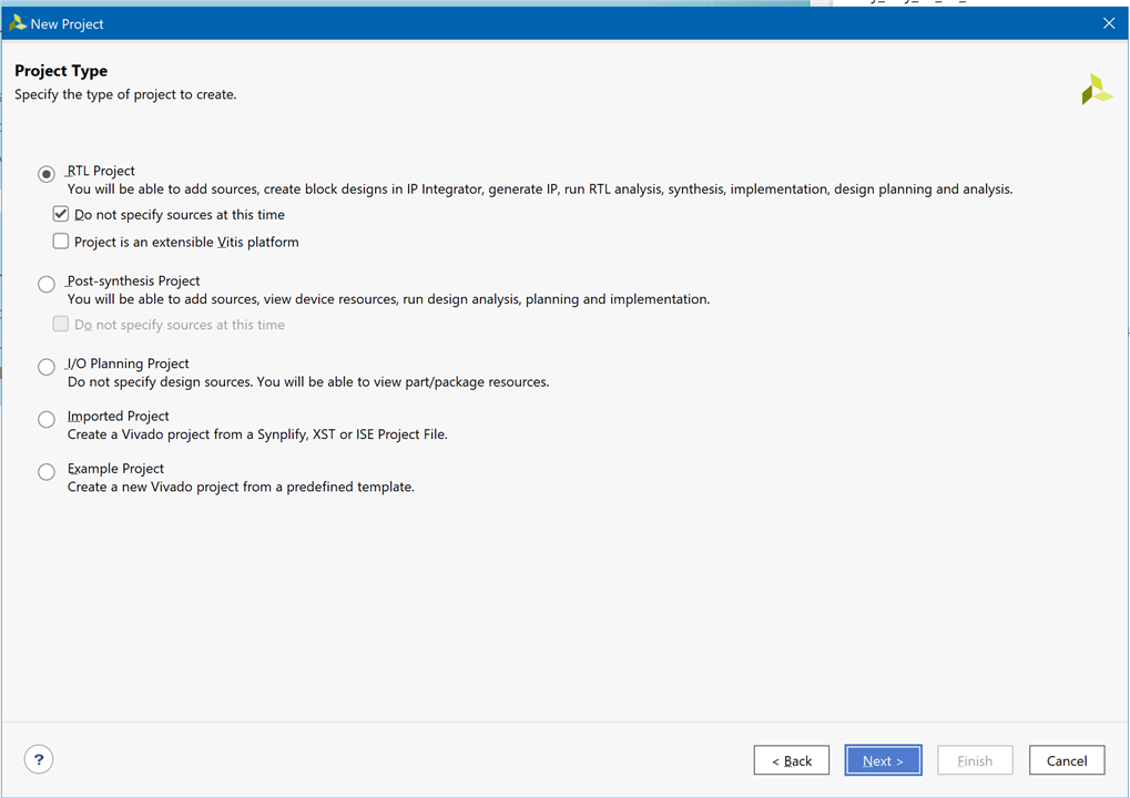
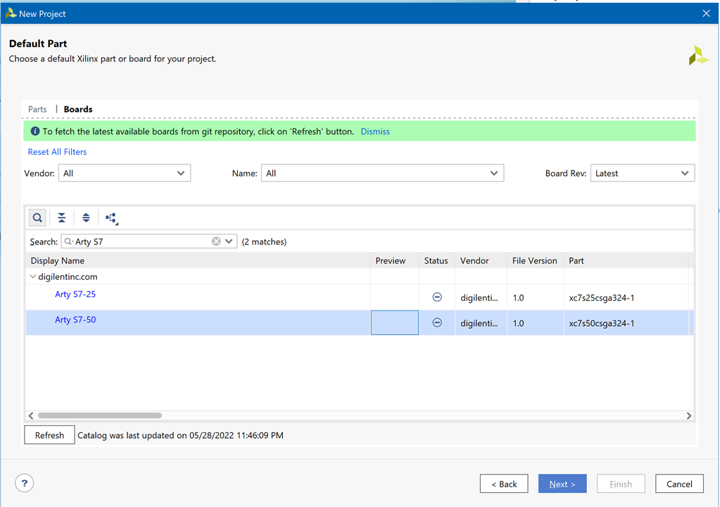
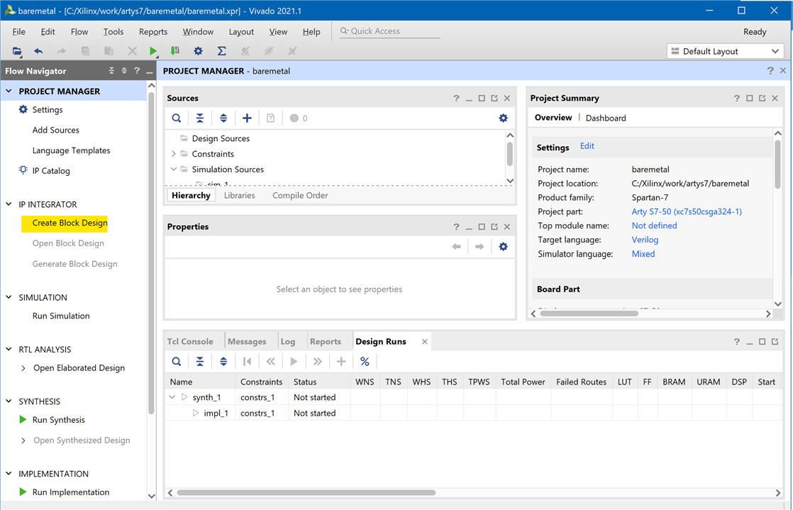
Create a Block Design from IP INTEGRATOR
Name your Block Design

Add a Microblaze Processor to the Block Diagram
When creating a design with DDR, it's best to add the DDR interface first, as it is typically also used to generate the clock or clocks that will be used by the rest of your design.
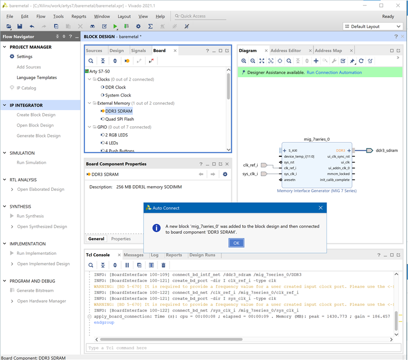
Go to boards section and right click on the DDR3 SDRAM and select Auto Connect

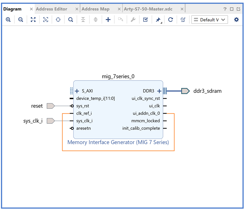
This process will add a MIG and the external DDR interface to the design. Two clock pins are also created, which will need to be modified.
Delete the “clk_ref_i” pin. This can be accomplished either by right-clicking on the pin and selecting delete or by selecting and pressing the delete key.
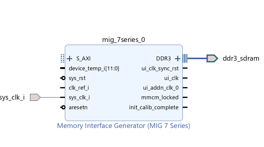
Select the "ui_addn_clk_0" pin and verify it has a frequency near 200 MHz
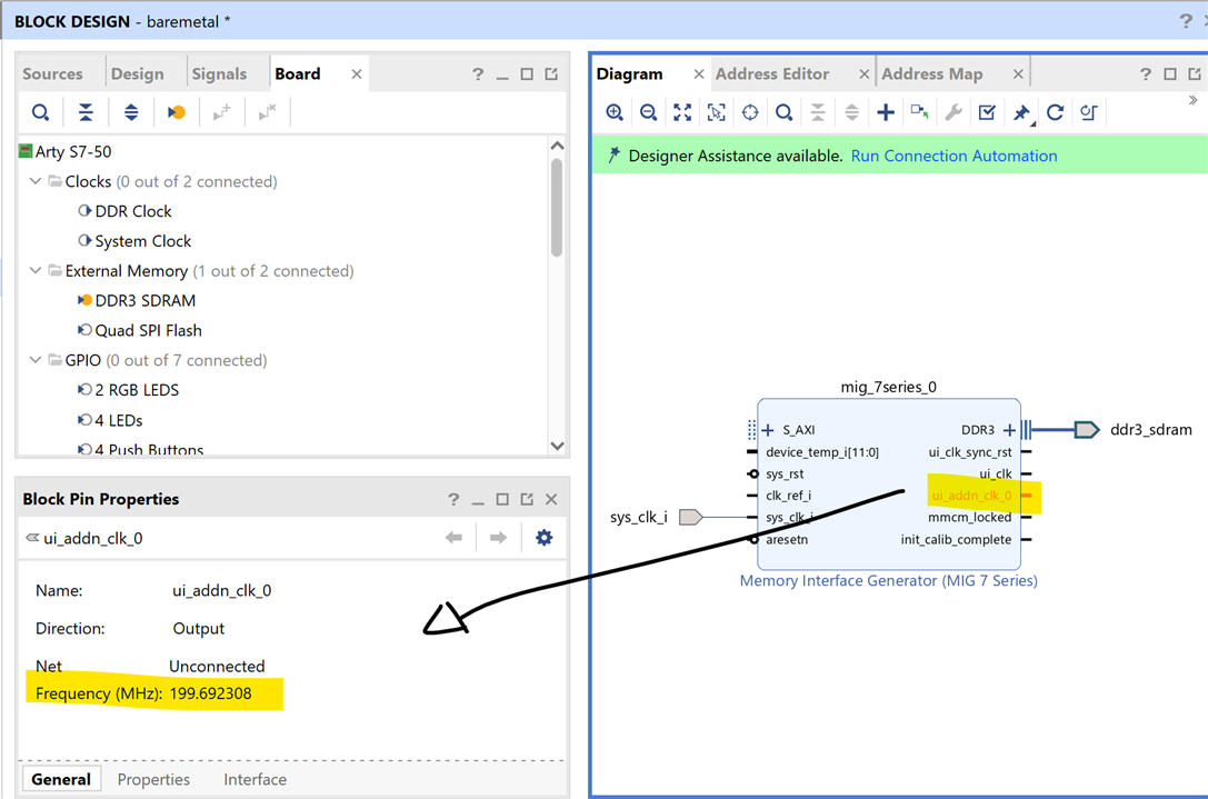
Connect the “ui_addn_clk_0” pin to the “clk_ref_i” pin by clicking and dragging from one to the other.

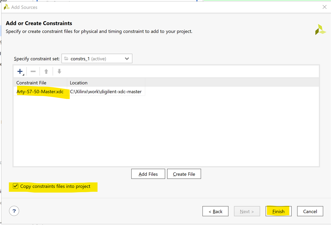
Add the Master XDC File
Master XDC files for Digilent boards contain pin constraints for I/O interfaces the board offers.
Download and extract digilent-xdc-master.zip. This file includes all of the latest template XDC files released for Digilent's boards, which are available on Github in the digilent-xdc repository. https://github.com/Digilent/digilent-xdc
This file contains the constraints that your board places on designs using it - specific interfaces wired up to specific pins, clock frequencies, and FPGA bank voltages, for some examples.
The constraints are sorted by interface.
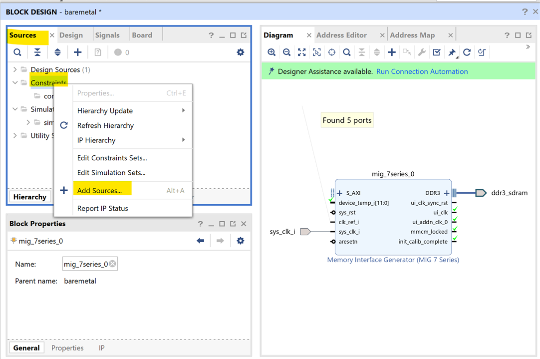
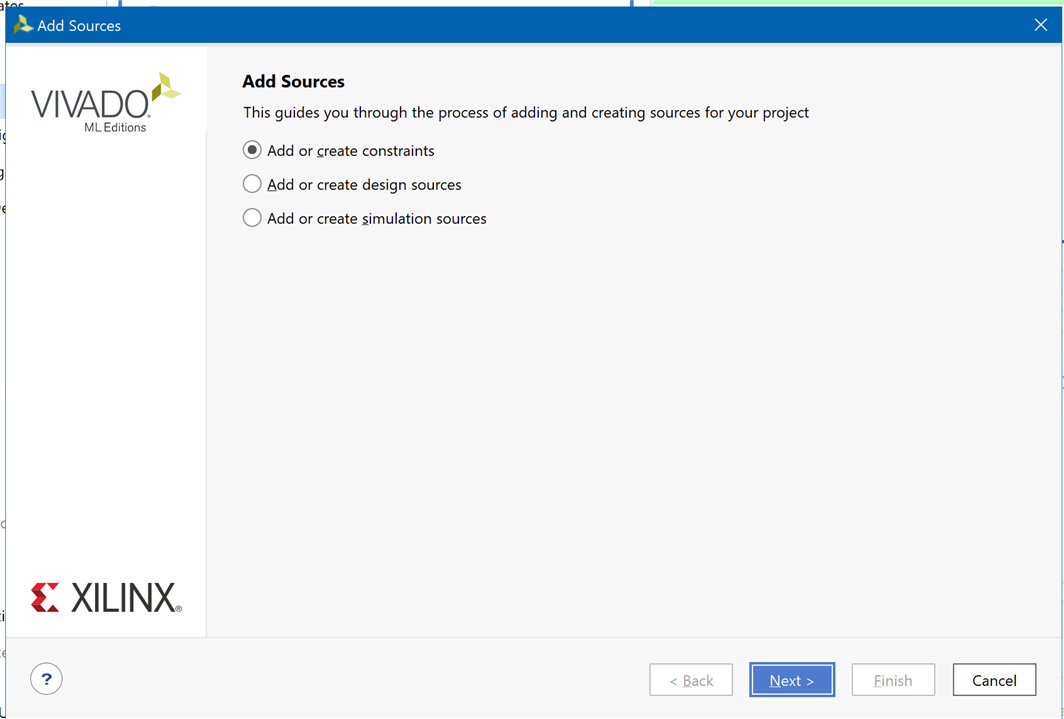
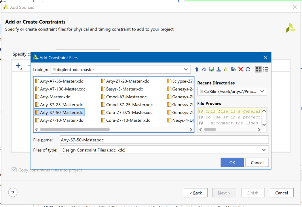
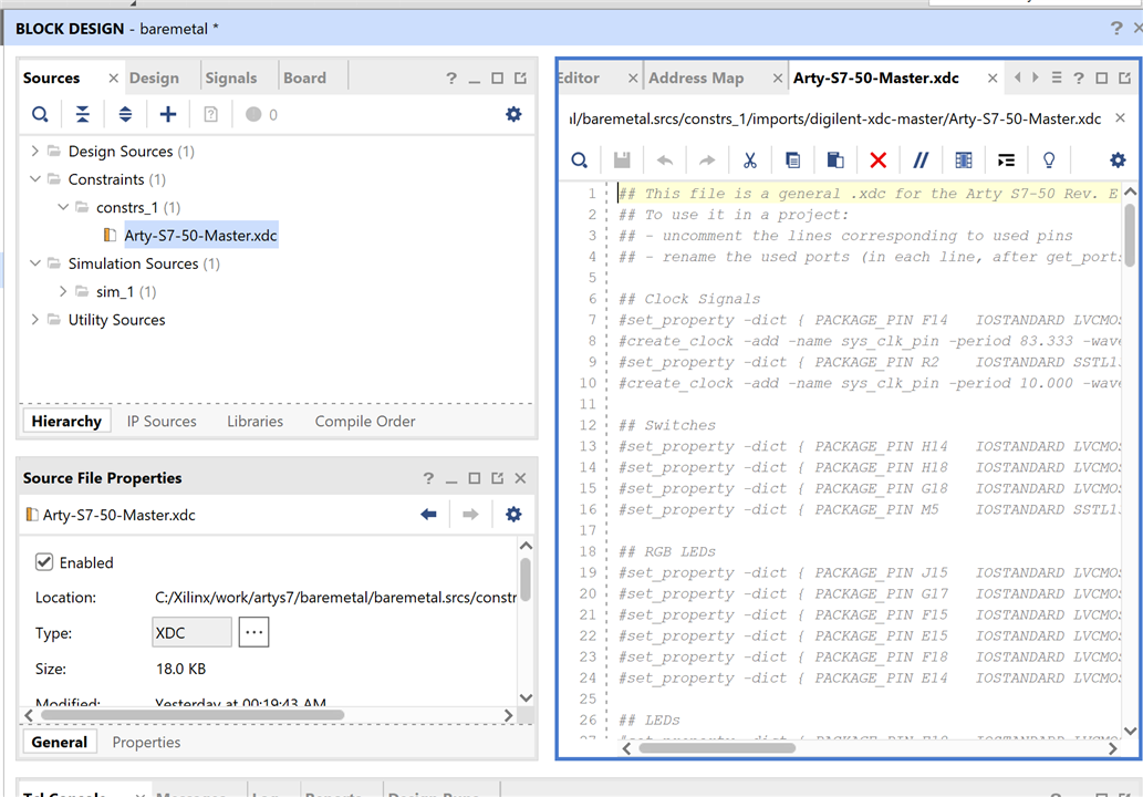
Find the set_property and create clock constraints for your board's 100 MHz input clock, uncomment them by removing the # at the start of each line, and change the name of the port that they are constraining to sys_clk_i, to match the name of the port in the block design.
Make sure to save your changes.

Next, the MIG's reset pin will be connected to the board's reset button. Click “Run Connection Automation” in the green bar at the top of the window.

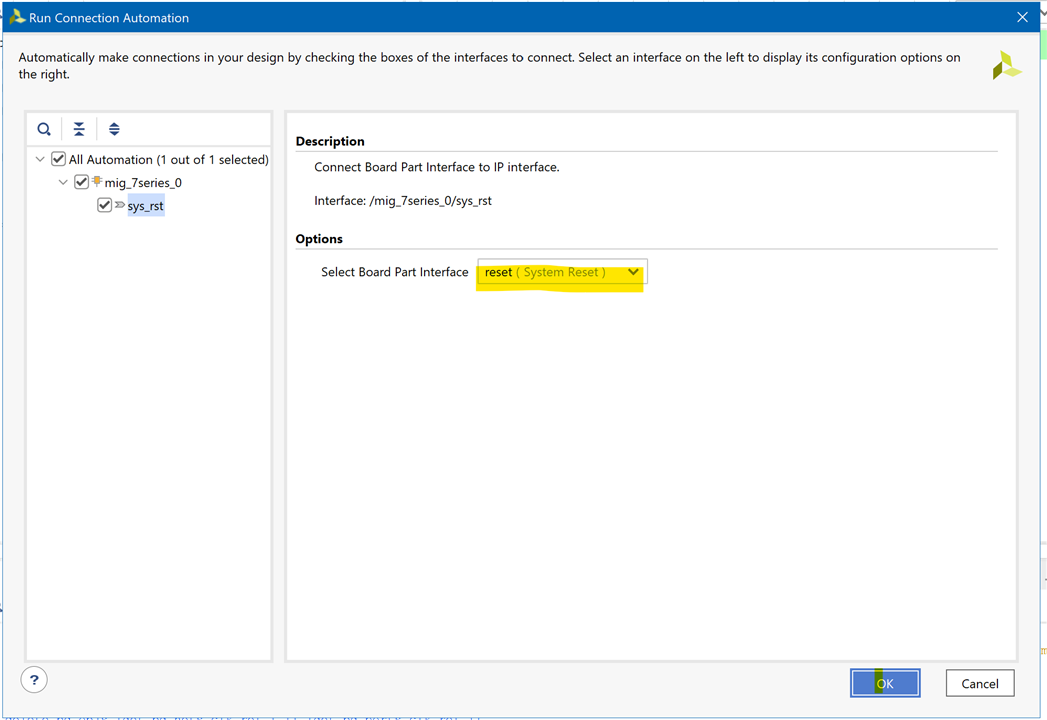
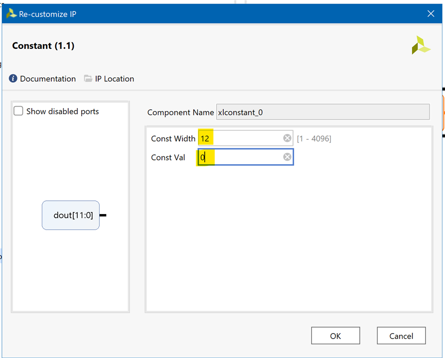
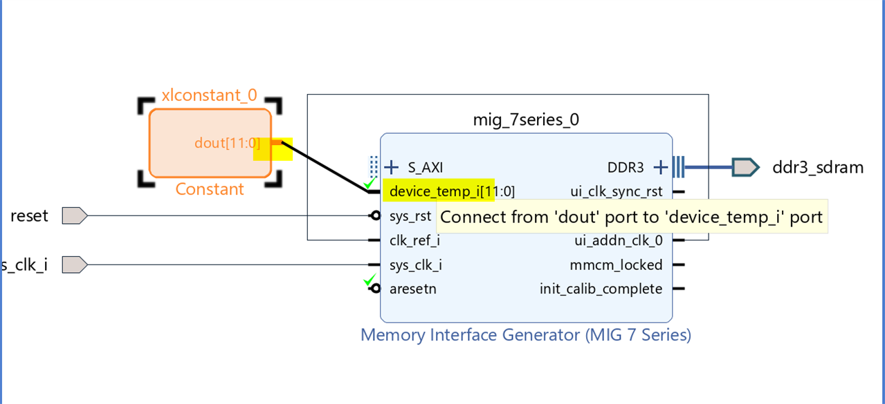
The MIG block has a “device_temp_i” port, it means that the MIG is not using the chip's XADC analog-to-digital converter feature. We'll ground this port to prevent any warnings that it may throw. Add a “Constant” IP to the design.

Double click on the block to open it's configuration wizard and modify it to have a Value of “0” and a Width of “12
Connect its output port to the “device_temp_i” port on the MIG.
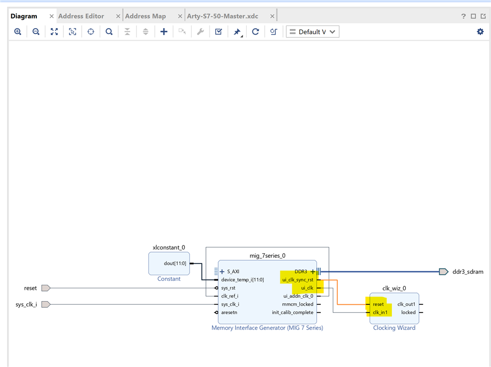
If your design requires more clocks than just the ui_clk provided by the MIG, you will need to add a clocking wizard IP that is driven by the MIG's ui_clk.
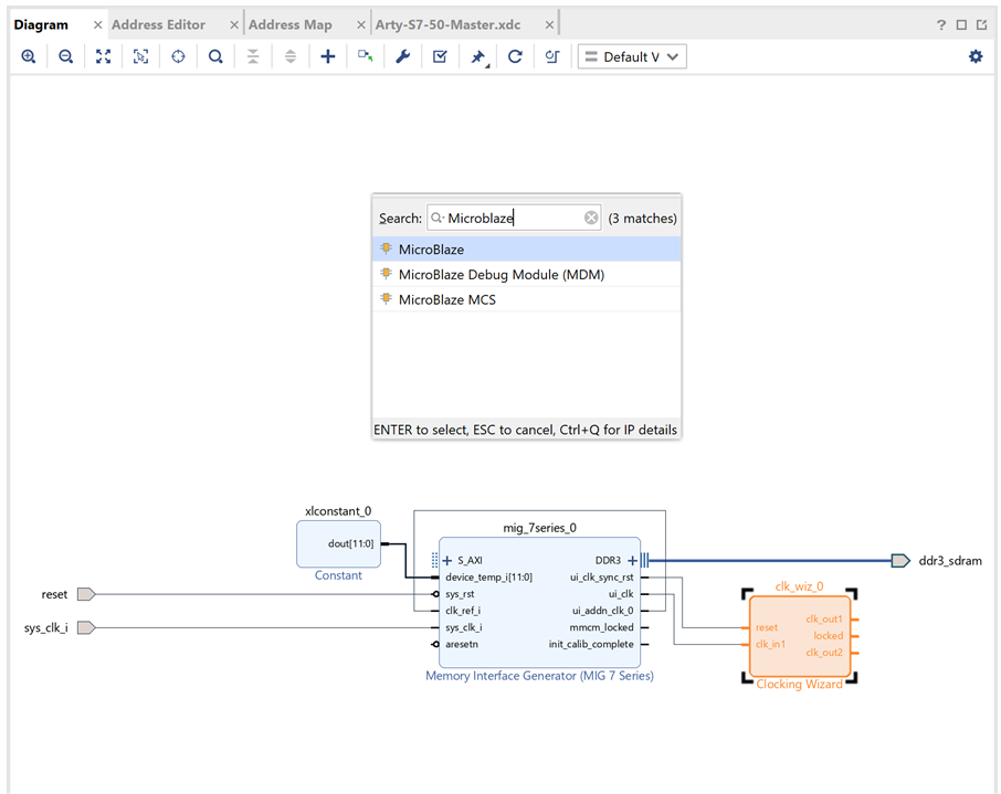
Use the Add IP button to search for and add a Clocking Wizard to the design.
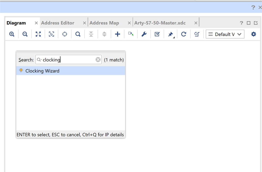
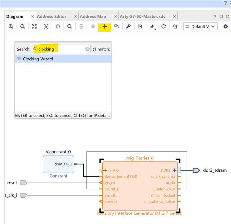
Manually connect the Clocking Wizard's clk_in1 and reset ports to the MIG's ui_clk and ui_clk_sync_rst ports, respectively.
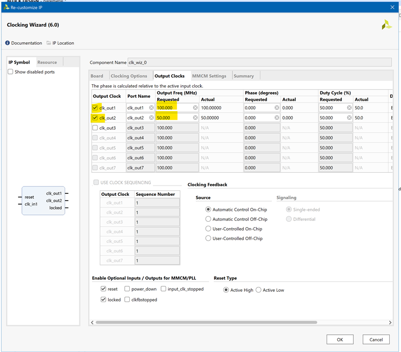
Finally, double-click on the Clocking Wizard to open and configure it. The third tab, Output Clocks contains all of the settings required to specify how many clocks you need, and of what frequencies. The screenshot to the right shows the wizard configured to create a 100 MHz clk_out1 and a 50 MHz clk_out2.
If your design requires additional clocks (such as for an ext_spi_clock pin), they should be added here. You don't need to add the second clock for this tutorial.
Add Microblaze IP
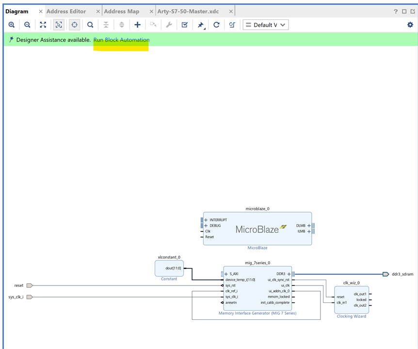
Next, use the Add IP button () to add the MicroBlaze IP to the design. The block that is added represents the core of the Microblaze processor.
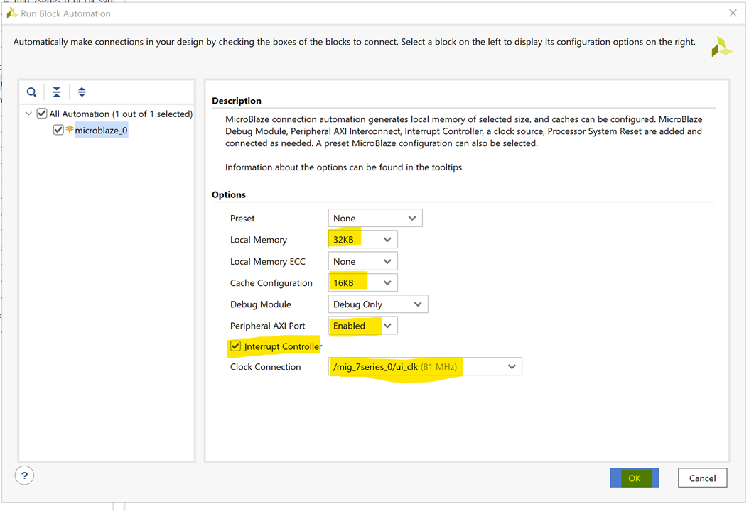
Next, block automation will be run so that additional supporting infrastructure can be added to the design. Click Run Block Automation in the green Designer Assistance bar.
In the Run Block Automation dialog, several settings can be specified for how the Microblaze IP will be connected to the rest of the design:
- Local Memory specifies how much block RAM memory will be dedicated to the processor. DDR-less designs require more memory, and the amount of memory necessary depends heavily on the size of the software application being run. 32KB is enough for many small applications.
- Cache Configuration can help the speed of designs using DDR memory. It should be enabled when using DDR, and disabled otherwise.
- Debug Module allows you to specify the capabilities of the debugger. The default Debug Only option is recommended.
- Peripheral AXI Port enables or disables the AXI master interface of the processor. It must be enabled to allow the processor to be connected to hardware peripherals.
- Interrupt Controller specifies whether the processor can be interrupted by its peripherals. Whether or not it needs to be enabled depends on your design requirements. If any IP that you intend to connect to the processor must have interrupts to function correctly, the box must be checked.
- Clock Connection specifies the processor's clock. Designs using DDR should use the MIG's ui_clk pin, while designs without DDR should use the Clocking Wizards clk_out1 pin.
Note: Settings not present in this list are out of the scope of this guide, and can safely be left as their default.
Confirm that the settings meet your design requirements. It should be noted that while it is possible to change these settings manually later (for example, by manually adding an AXI INTC IP and connecting it to the processor), the easiest way to do so will be to clear the Microblaze processor out of your block design and restart the process of adding the processor. This is to say, the settings chosen here are important. Getting them right the first time will save you time in the long run.
Important! When working with multiple clocks in a design (as happens to always be the case when working with the MIG) it is important to verify that you are picking the correct Clock Connection from the dropdown. In the screenshot to the right, the 100 MHz clk_out1 from a clocking wizard is chosen. You may instead wish to run your design off of ui_clk itself. Do not select the system clock input to the MIG.
Click OK to continue.
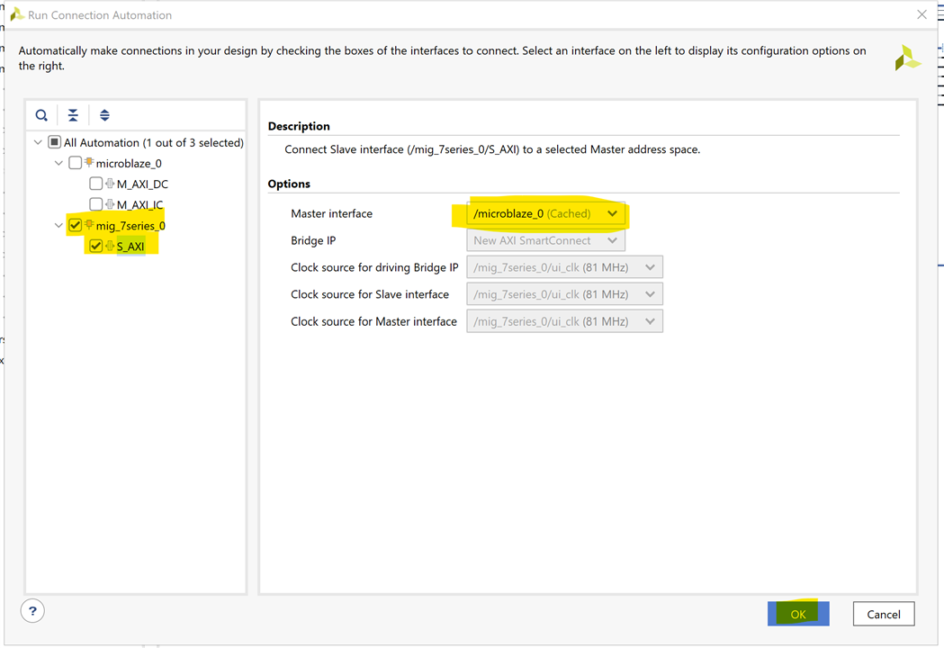
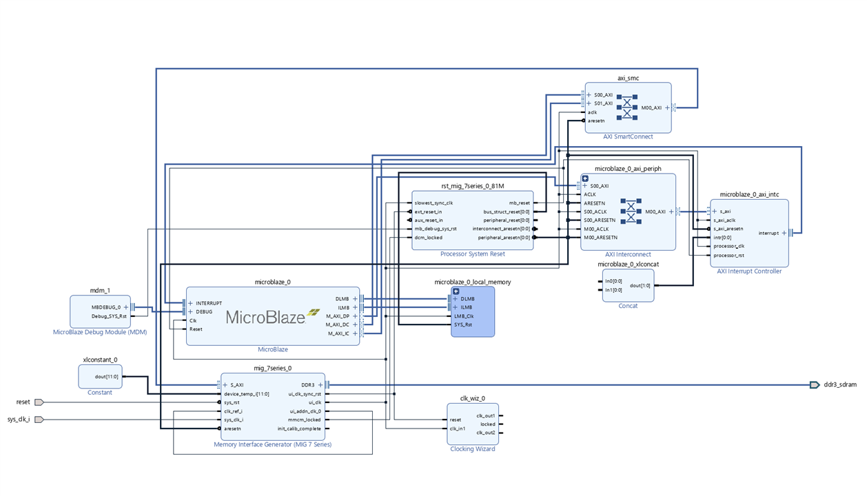
Next, the MIG's AXI interface must be connected to Microblaze's cache ports, in order to allow data to move back and forth between processor and DDR memory.
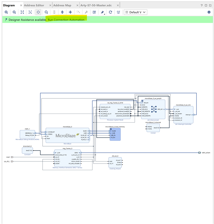
To connect the MIG's AXI interface to the processor, click the Run Connection Automation button in the green banner at the top of the block design.
In the dialog that pops up, you will be presented with several options for interfaces that can be connected to other interfaces. Both the Microblaze's IC and DC ports, as well as the MIG's AXI port will appear. You should only run connection automation for one side of the connection - the S_AXI port, as shown in the screenshot to the right. Make sure that its box is checked. Check that the Master interface is set to “/microblaze_0 (Cached)”, indicating that the microblaze local memory will act as a cache for the DDR memory, then click OK to make the connections.
Connect USB UART peripheral
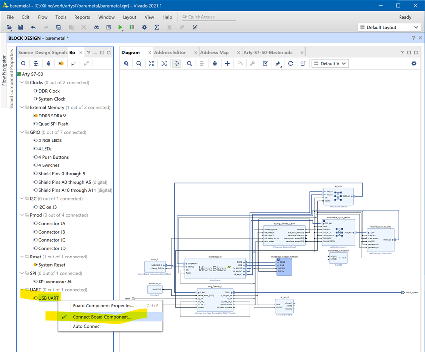
Next, in order for the software design to be able to print to a serial console on a host computer, a UART peripheral must be connected. Find the USB UART interface in the Board tab, right click on it, and select Connect Board Component.
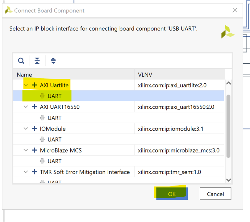
In the dialog that pops up, select a new AXI Uartlite IP's UART interface, and click OK to add the block to the diagram.
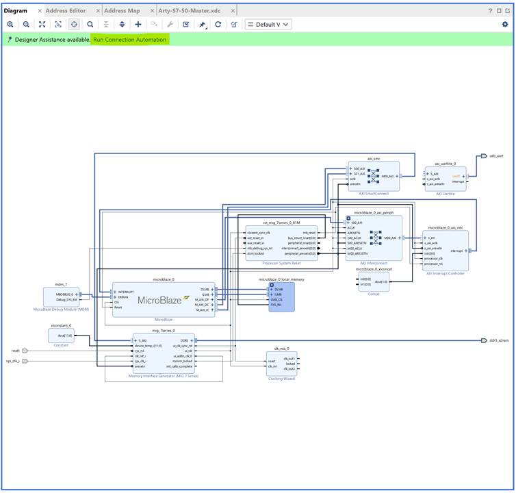
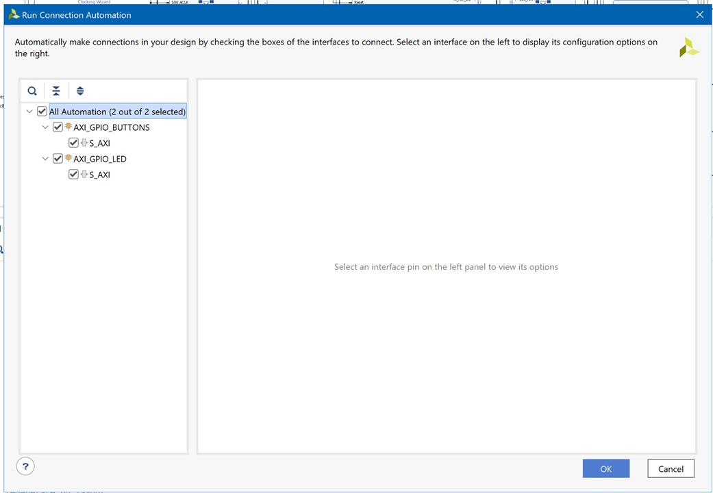
To connect all remaining AXI cores that have not yet been connected to the processor, click the Run Connection Automation button in the green Designer Assistance bar.
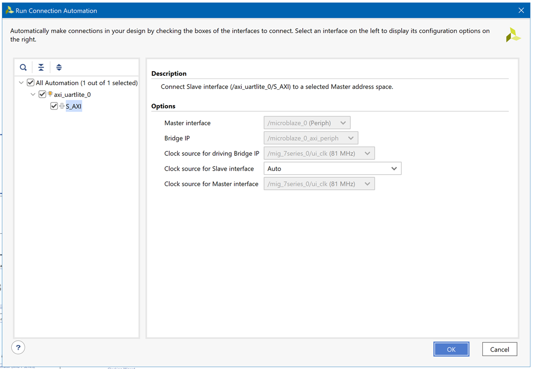
Check the All Automation box in the list on the left side of the window to select all of the remaining AXI cores. The dropdown settings available for each core can safely be left as their default values. Click OK to automatically connect them to the processor.
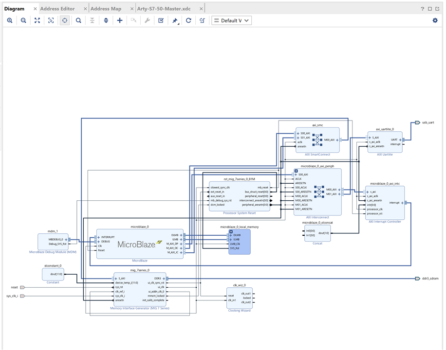
Add GPIO Peripherals to a Block Design
Two methods:
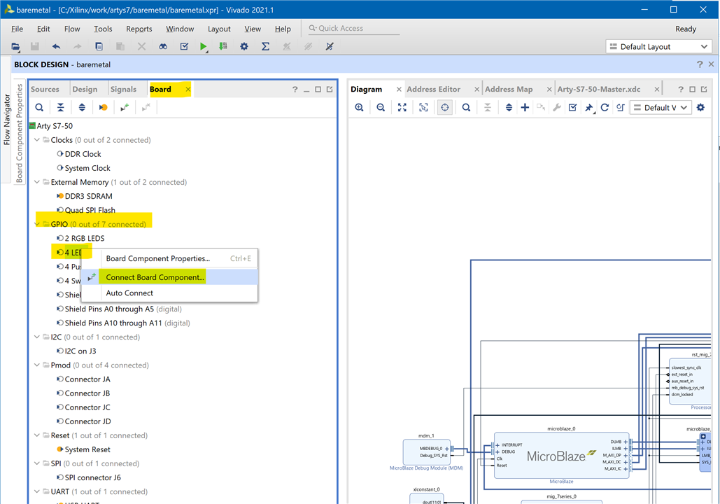
- Using board files to automatically generate constraints: Interfaces for Digilent boards supported by the board files can be found in the Board tab.
- IP connected to chosen pins manually
Using board files
Find the GPIO section of the list, right click on an LED interface, and select the Connect Board Interface option.
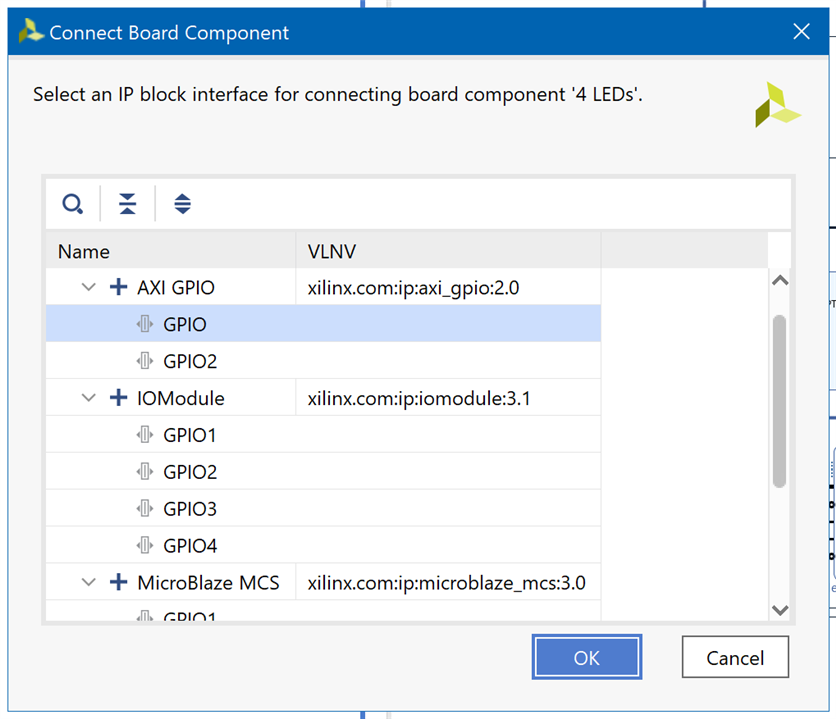
In the dialog that pops up, choose the “GPIO” interface (not GPIO2) of a new AXI GPIO IP.
Click OK to continue. This will add the IP to your design, and connect it to an external port, which will not require any further work to constrain.
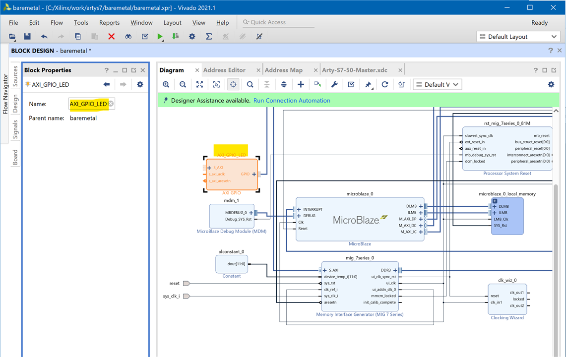
Next, select the axi_gpio_0 block. The Block Properties pane to the left of the Diagram and below the Board tab will allow you to view some information about the block, and modify it in some ways, without running through its customization wizard.
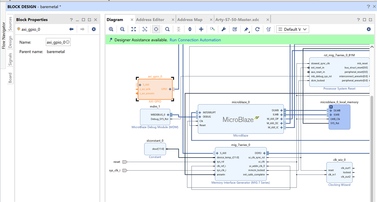
Change its name to “AXI_GPIO_LED” by typing in the Name field. Pressing enter or clicking out of the text box confirms the change. Using memorable names in your block design makes it easier to remember which IP does what when you are later writing software in Vitis.
IP connected to chosen pins manually
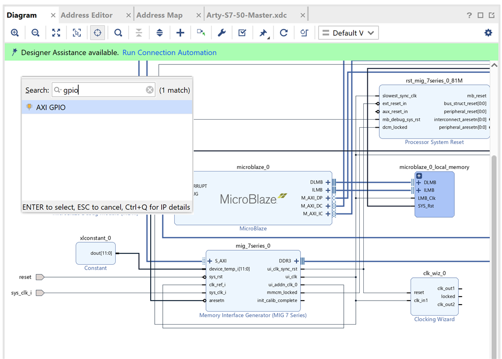
A second AXI GPIO IP will be manually added to the block diagram, and manually constrained with an XDC file.
Click the Add IP button (+) and search for “AXI GPIO”. Double click on the only result to add the second AXI GPIO block to the design.
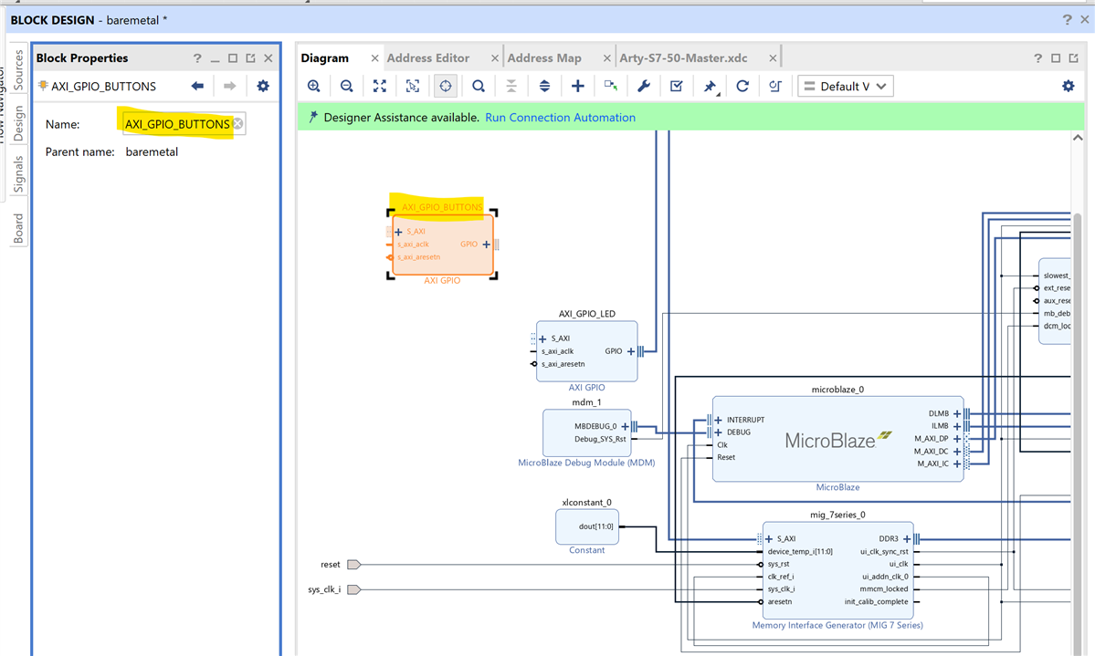
Once added, rename this IP “AXI_GPIO_BUTTONS”
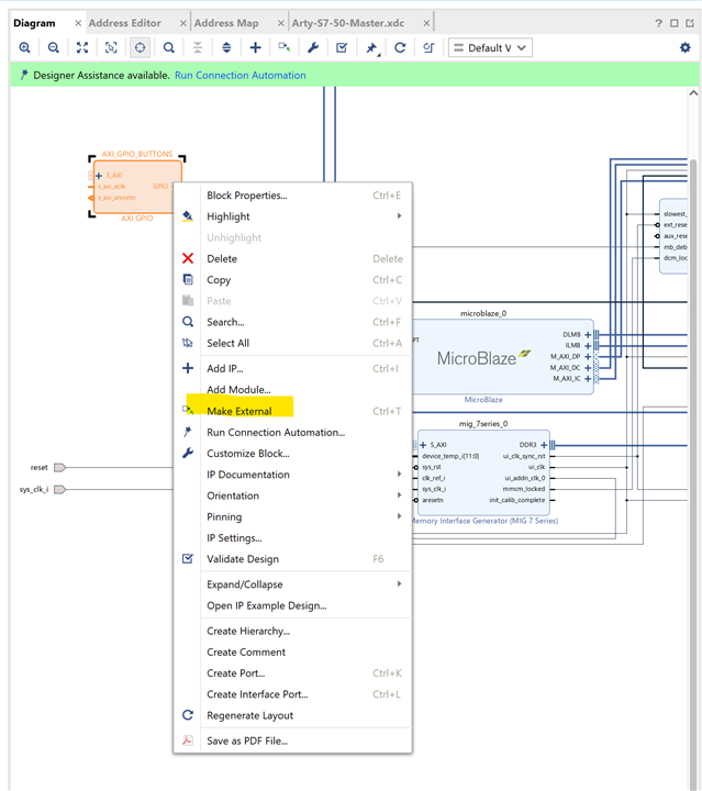
Select the AXI_GPIO_BUTTONS IP's GPIO interface by clicking on the text “GPIO”, right click on the highlighted text, and select Make External. This option creates a new external interface port that does not rely on the board files. Because the board files are not used here, a Xilinx Design Constraint (XDC) file must be added to the project to tell Vivado which FPGA pins to connect the interface to.
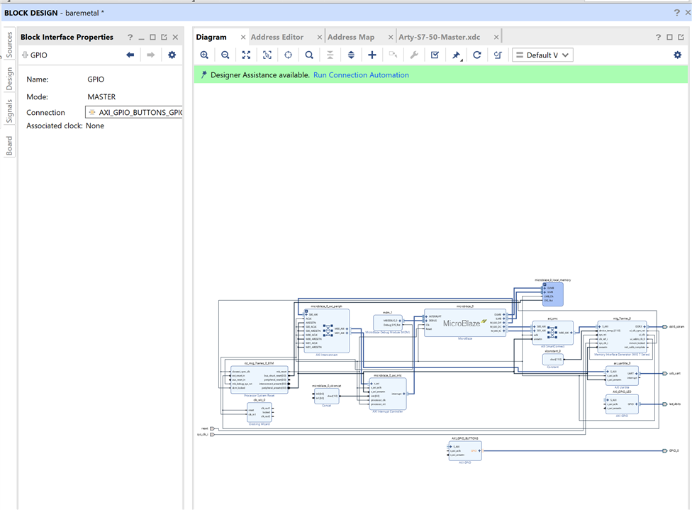
Edit the previously Master XDC File imported.
Master XDC files for Digilent boards contain pin constraints for I/O interfaces the board offers. These constraints are sorted by interface. Scroll down until you see constraints for the user buttons. These constraints typically are for a bus port named “btn”. Un-comment the button constraints by removing the single leading '#' character in each line corresponding to the buttons.
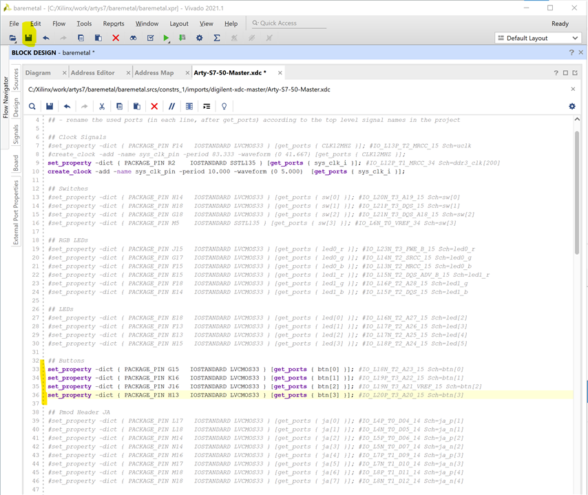
the names of the block design's GPIO port for the buttons must be determined, so that the buttons can be properly constrained. Reopen the Diagram tab, and select the GPIO_0 external port that is connected to the AXI_GPIO_BUTTONS block. Change the name of the external interface to “btn” in the Properties pane.
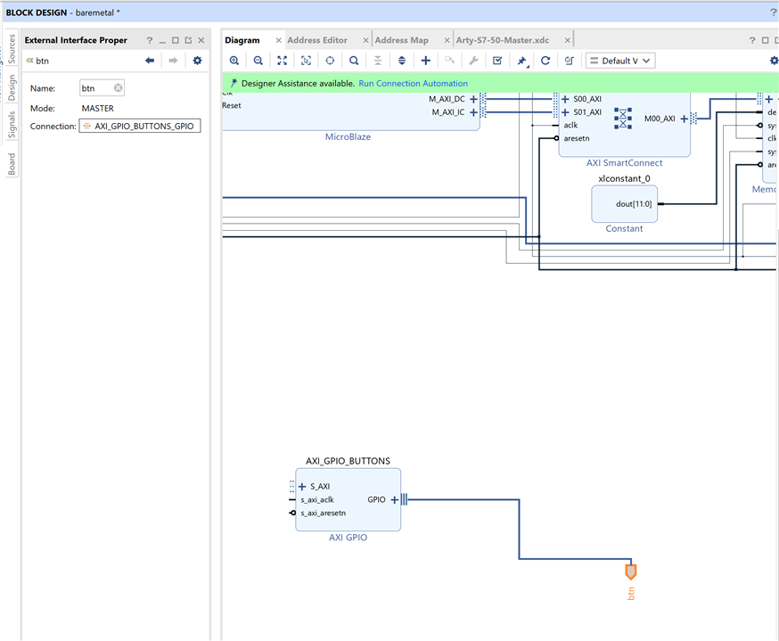
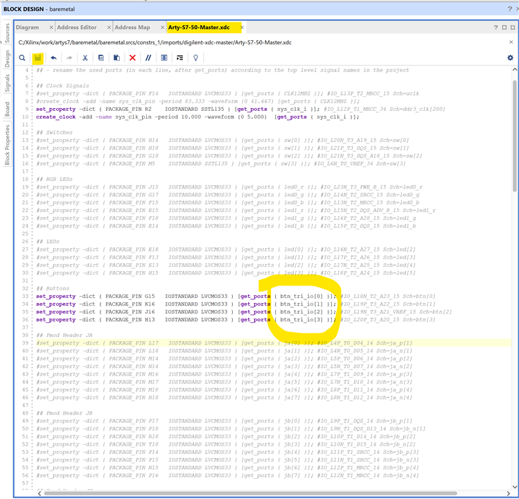
The AXI GPIO IP automatically uses tri-state buffers for the pins its interfaces are connected to. The individual I, O, and T buses can be seen when expanding the interface through the plus button (+) next to the interface name on the IP block. As can be seen, the individual ports that make up the interface are named <interface>_tri_i, <interface>_tri_o, and <interface>_tri_t. When constrained to tristate buffers, the bus that is connected to FPGA ports is named <interface>_tri_io.
Return to the XDC file, and change the name of the button bus that is constrained. Specifically, change the text after the “get_ports” call on each line of the button interface to “btn_tri_io[#]”, where # is a decimal number, counting up from zero. When finished, save the file.
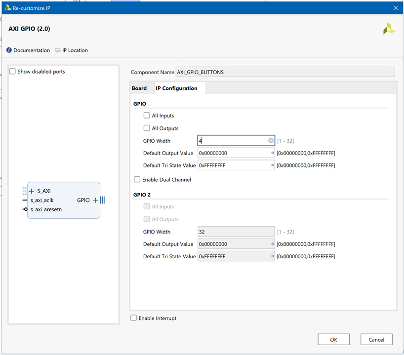
With the constraints for the port finished, the AXI GPIO must be manually configured. In particular, the width of the GPIO interface must match the number of buttons available on the board. Take note of how many buttons are constrained in the XDC.
Return to the Diagram tab, and double click on the AXI_GPIO_BUTTONS block. This will open a dialog that will allow you to configure the IP's settings. Switch to the configuration wizard's IP Configuration tab.
Only one setting need be changed for the purposes of this guide. Enter the number of buttons you constrained into the GPIO interface's GPIO Width field. When finished, click OK to save your changes.
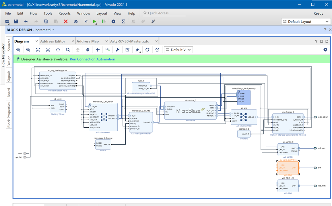
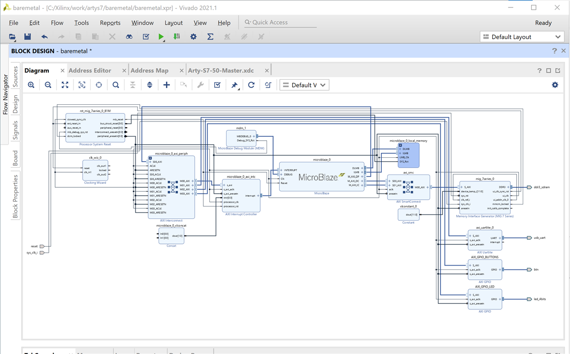
Finally, the two AXI GPIO IP blocks need to be connected to the processor in your design. Click the Run Connection Automation button in the green Designer Assistance bar.
Review the address map
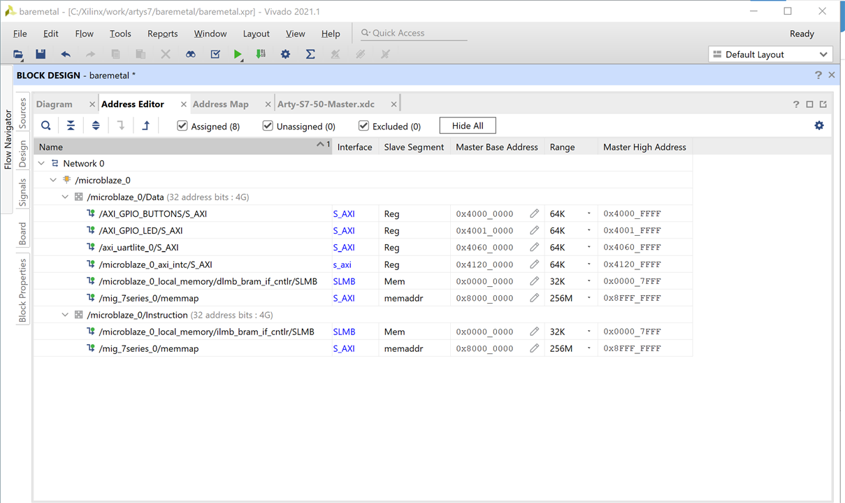
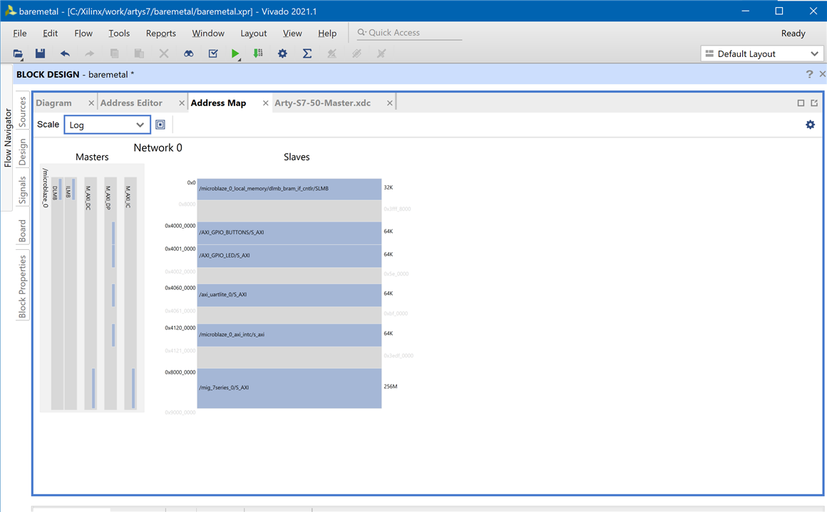
In the unlikely event that Vivado fails to correctly assign addresses to each AXI IP connected to your processor, you may need to manually set their addresses. If this occurs, errors will pop up during validation of the block design, and the bitstream will not be able to be generated.
The Address Editor can be accessed through its tab in the Diagram pane. Addresses can be assigned to unmapped peripherals by typing the desired address into the peripheral's Master Base Address column.
It should be noted that addresses must be aligned in the memory space - for instance, an address with a range of 4K (bytes) takes up a range of 0x1000 addresses, and must have three trailing zeros. Address ranges for different segments cannot overlap.
Assigning an segment to address 0 may result in assertions in some software drivers and should be avoided.
After manually assigning addresses, the block design should be re-validated.
Validate Block Design
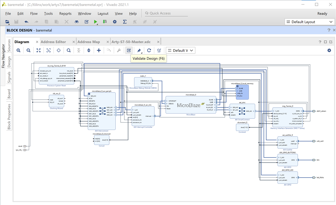
Before the Vivado project can be built, the block design must be validated. This step runs an automatic check of the block design to see if there are any potential issues with it. Click the Validate Design button () in the Diagram pane's toolbar (or press the F6 key).
If the design has issues, a dialog will pop up that lists them. It should be noted that most Warnings can be ignored, as can some Critical Warnings. These issues can also be viewed in the Messages tab of the pane at the bottom of the window.

Create an HDL Wrapper
Additionally, an HDL wrapper must be created for the block design. This process translates the block design into a source file that can be read by the Vivado tools, and is used to build the actual design.
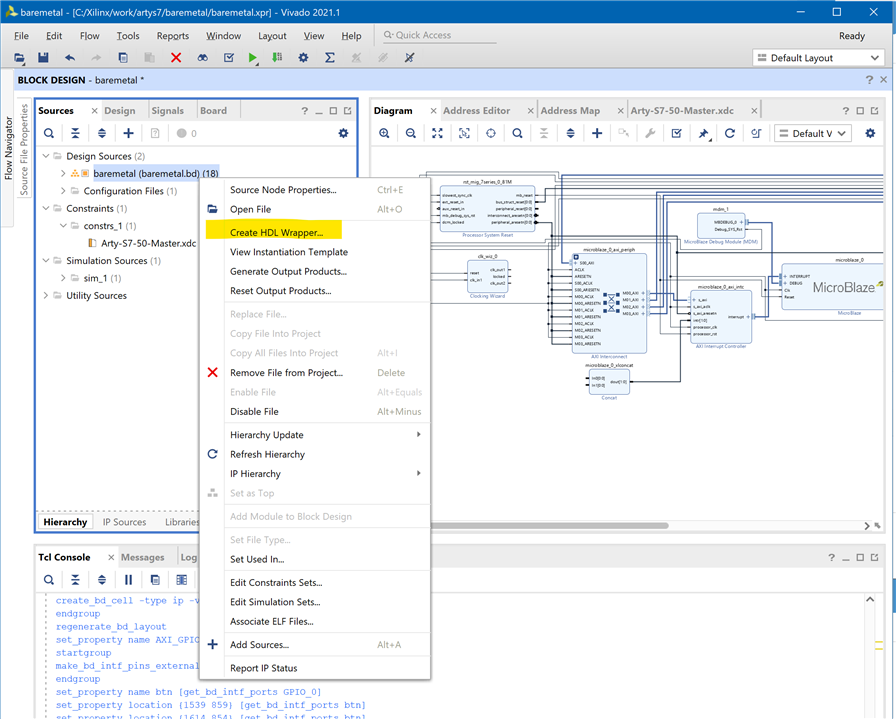
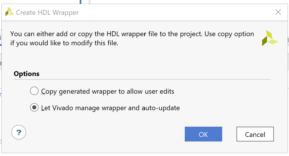
Open the Sources pane and locate the block design file (.bd) under the Design Sources dropdown. Right click on it and select Create HDL Wrapper.
In the dialog that pops up, you can decide whether to let Vivado edit the wrapper file itself. Let Vivado manage wrapper and auto-update is recommended, as a user rarely needs to manually edit the wrapper file. Click OK to continue.
Build the Vivado Project
Click the Generate Bitstream button in the Program and Debug section of the Flow Navigator pane at the left side of the window.
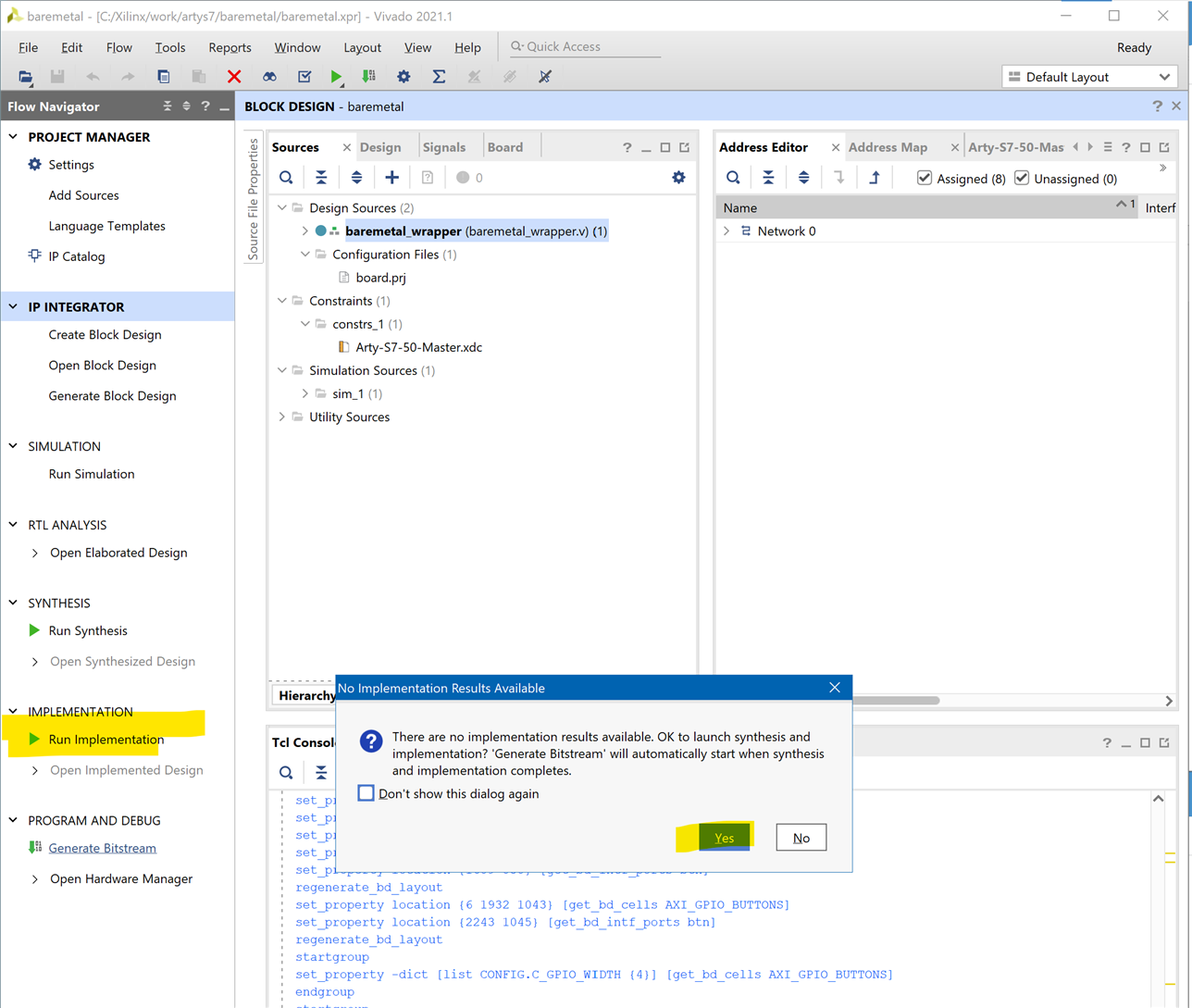
A dialog will pop up with several options for how Synthesis and Implementation should be run. Most should be left as defaults. Of particular importance is the Number of jobs dropdown, which is used to specify how much of the resources of your computer should be dedicated to the build. A larger number of jobs will dedicate more resources, which will allow the build to be completed faster. It is recommended to choose the highest available number.

When complete, a dialog will pop up that presents several options for what to do next:
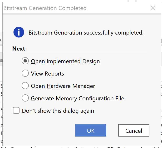
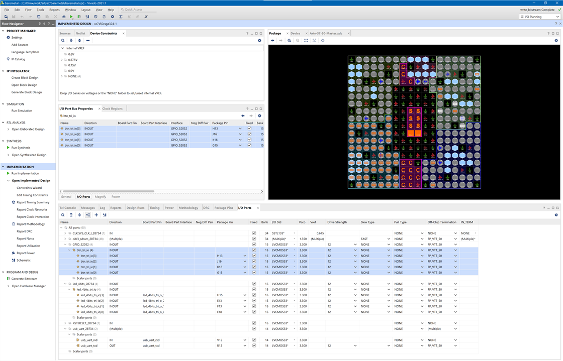
- Open Implemented Design can be used to view the actual hardware design that has been implemented and will be placed onto the chip.
- View Reports can be used to view additional information about the design, including how much of the resources of the FPGA will be used by the design.
- Open Hardware Manager can be used to go directly to Vivado's Hardware Manager, which can be used to program a hardware design onto a board. This is typically used for designs that do not involve a software component.
- Generate Memory Configuration File can be used to create a file for programming an FPGA-only design into flash memory.
If none of these options are desired, click Cancel to continue.
Export a Fixed Post-Synthesis Hardware Platform
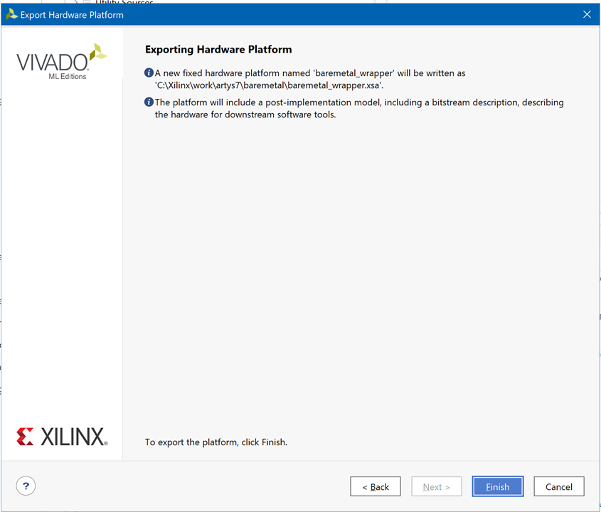
Once the project has been built, the design must be exported from Vivado so that Vitis has access to information about the hardware that a software application is being developed for. This includes the set of IP connected to the processor, their drivers, their addresses, and more. Exporting hardware after the bitstream has been generated allows you to program your board directly from within Vitis.
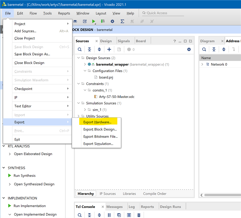
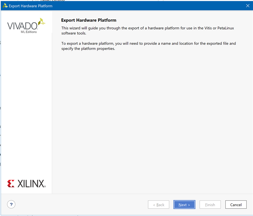
To export the hardware design, click Export → Export Hardware in the File menu.
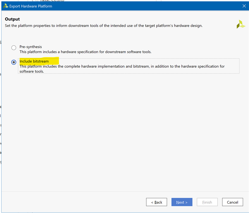
The Output screen allows you to select whether only the hardware specification (Pre-synthesis) should be exported, or whether the bitstream should be included. Since the bitstream has already been generated, it should be included in the platform so that Vitis can automatically figure out where it is when programming a board. Select Include bitstream and click Next to continue.
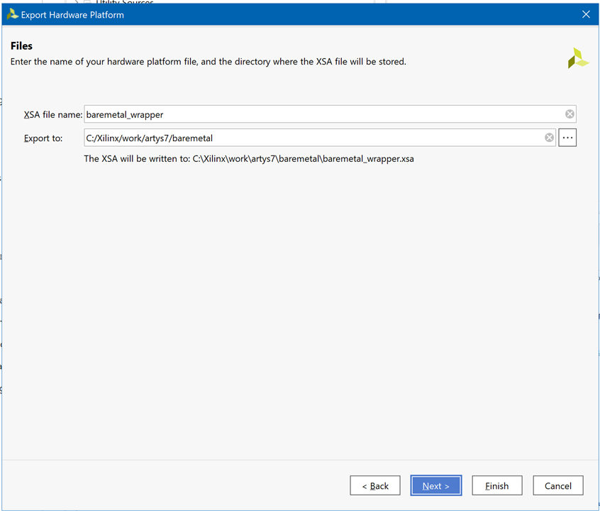
The Files screen gives you the option to choose a name for the Xilinx Shell Architecture (XSA) file, and provide a path to a folder that the file will be placed within. Give your XSA file a name, and choose a memorable location to place it in. This file will later be imported into Vitis, so take a note of where it is placed and what it is called.
Important: Do not use spaces in the file name or export path. Underscores or camelCase are recommended instead.
Click Next to continue.
Software Development
Launch Vitis to Program
It is a known issue that launching the Vitis IDE from the Vivado Tools menu does not work with Windows 10 and Vivado version 2021.1
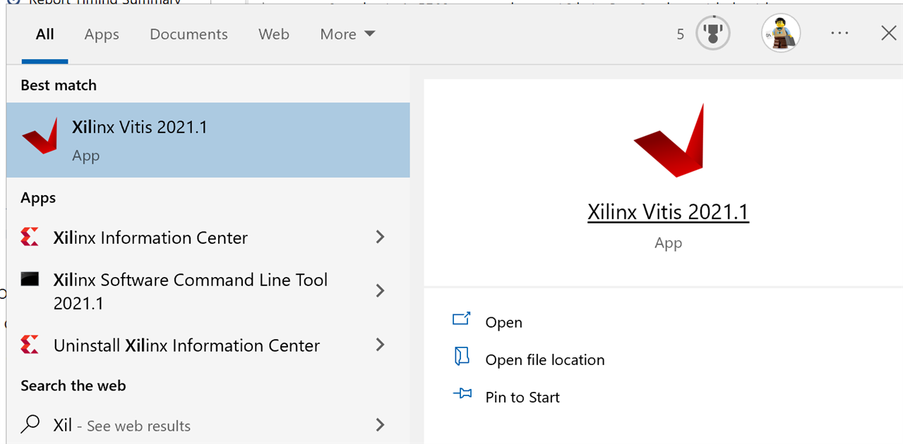
Open Vitis through the start menu or desktop shortcut created during the installation process.
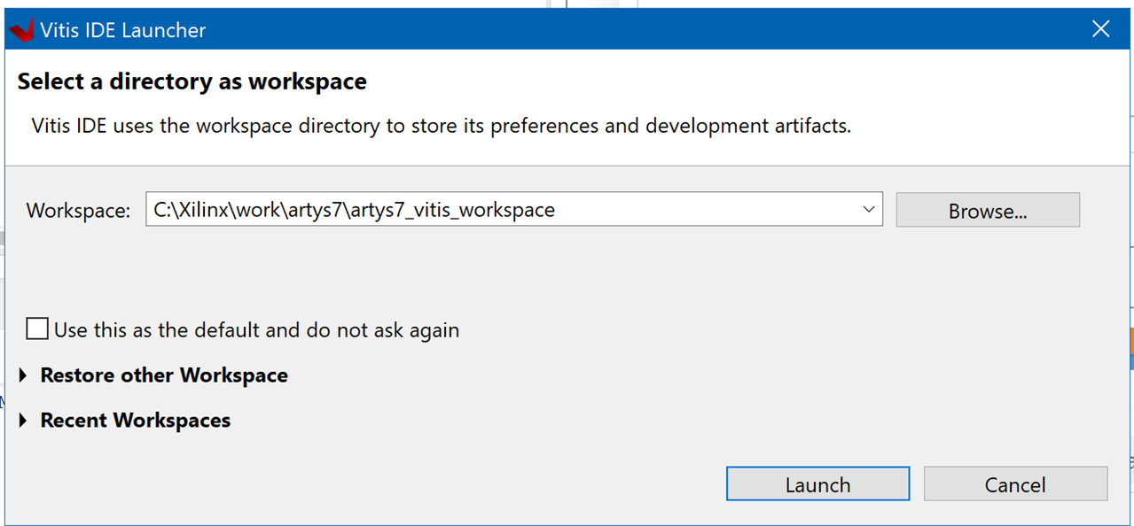
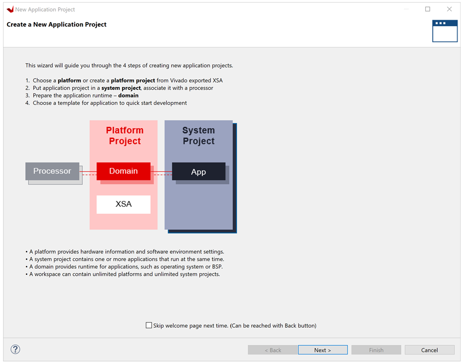
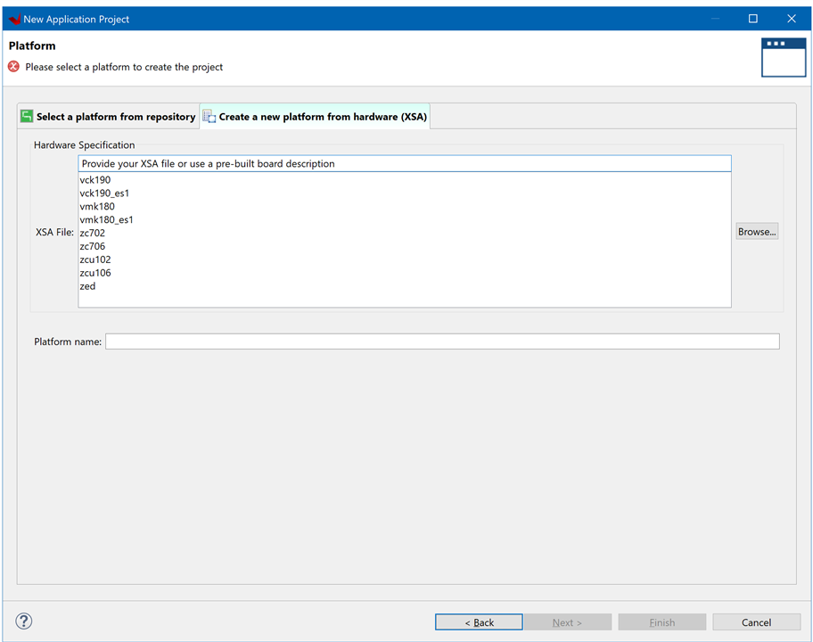
Next, the platform that the application targets must be created. Open the Create a new platform… tab.
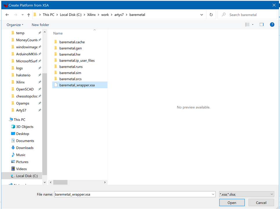
Browse your file system to find the Xilinx Shell Architecture previously exported from Vivado. With the XSA file highlighted, click Open to select it and return to the Platform screen of the wizard.
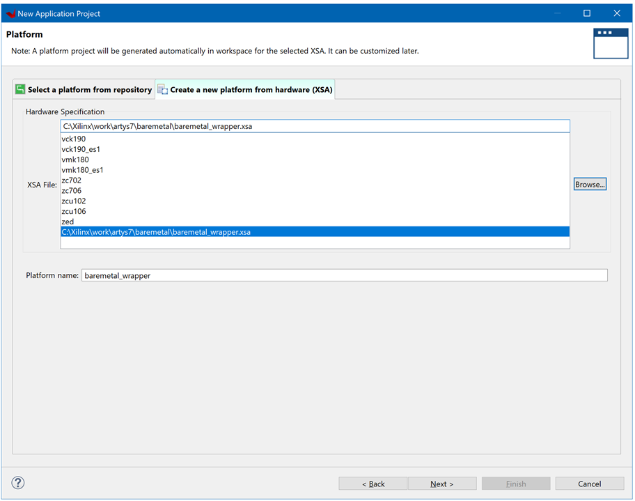
The next screen is used to set some options for the application project and the system project. The names of both projects can be set, as well as which processor core will be used to run the application. All settings can be left as defaults. Click Next to continue.
Note: A system project can contain multiple application projects, which can all be run at once.

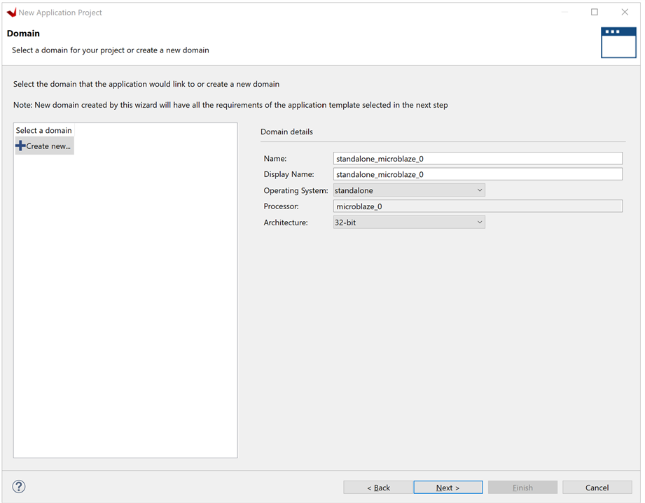
Next, the domain that the application project operates in will be defined. In this case all default settings will be used. Click Next to continue.
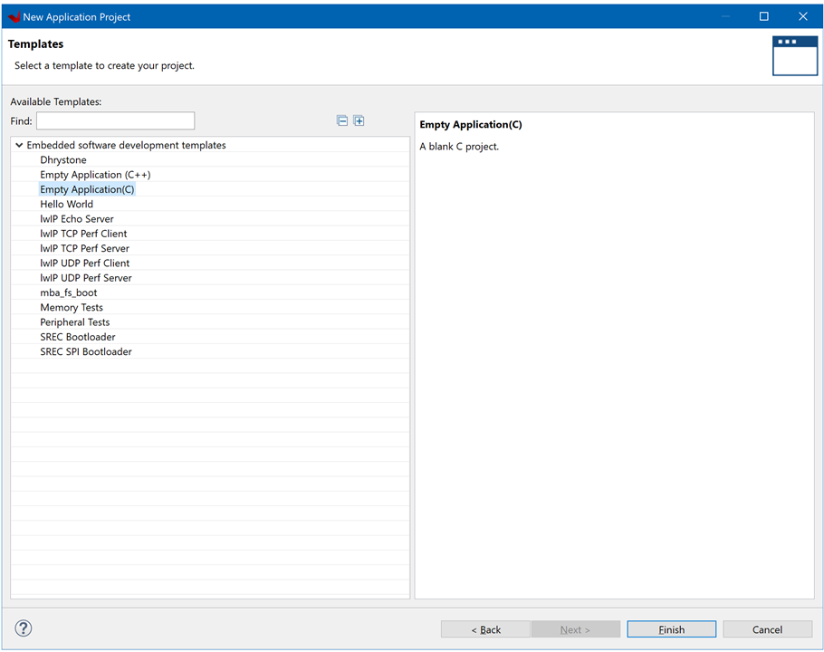
Lastly, a template project will be chosen. Each template pre-configures the application project for a different purpose. Depending on the whether your application will be written in C or C++, choose Empty Application or Empty Application (C++). You will be adding an example main source file later, as opposed to working from and editing an example.
Click Finish to finish creating the project.
Create a main.c Source to Control AXI GPIO Peripherals
In Vitis' Explorer pane, find the application projects “src” directory. Right click on it and select New → File
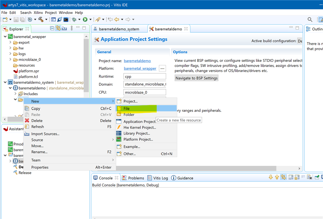
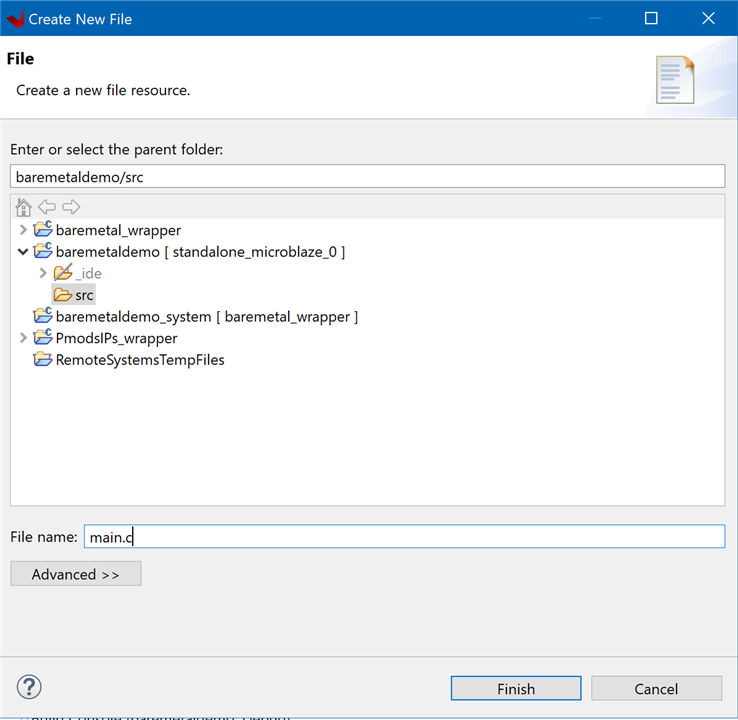
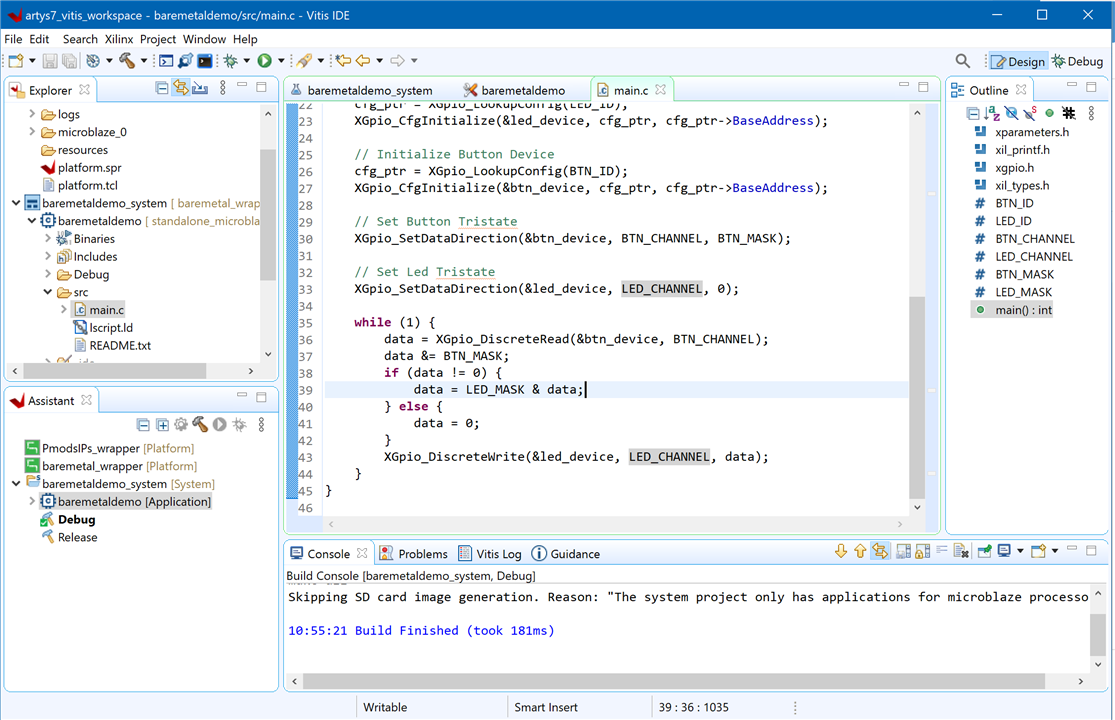
Copy and paste the code to the right into the empty main.c file that has now been opened.
#include "xparameters.h"
#include "xil_printf.h"
#include "xgpio.h"
#include "xil_types.h"

// Get device IDs from xparameters.h
#define BTN_ID XPAR_AXI_GPIO_BUTTONS_DEVICE_ID
#define LED_ID XPAR_AXI_GPIO_LED_DEVICE_ID
#define BTN_CHANNEL 1
#define LED_CHANNEL 1
#define BTN_MASK 0b1111
#define LED_MASK 0b1111

int main() {
	XGpio_Config *cfg_ptr;
	XGpio led_device, btn_device;
	u32 data;

	xil_printf("Entered function main\r\n");

	// Initialize LED Device
	cfg_ptr = XGpio_LookupConfig(LED_ID);
	XGpio_CfgInitialize(&led_device, cfg_ptr, cfg_ptr->BaseAddress);

	// Initialize Button Device
	cfg_ptr = XGpio_LookupConfig(BTN_ID);
	XGpio_CfgInitialize(&btn_device, cfg_ptr, cfg_ptr->BaseAddress);

	// Set Button Tristate
	XGpio_SetDataDirection(&btn_device, BTN_CHANNEL, BTN_MASK);

	// Set Led Tristate
	XGpio_SetDataDirection(&led_device, LED_CHANNEL, 0);

	while (1) {
		data = XGpio_DiscreteRead(&btn_device, BTN_CHANNEL);
		data &= BTN_MASK;
		if (data != 0) {
			data = LED_MASK & data;
		} else {
			data = 0;
		}
		XGpio_DiscreteWrite(&led_device, LED_CHANNEL, data);
	}
}
This code pulls in several headers that are automatically pulled into the Vitis workspace:
- xparameters.h is a file generated during the process of exporting a platform from Vivado. It includes information on the hardware design, including addresses and some configuration parameters for AXI IPs. This is used by the example code to find the device IDs that must be passed to the GPIO drivers, so that they can look up the driver configuration required to correctly initialize the GPIO devices.
- xil_printf.h gives access to the xil_printf function, which can be used to print to standard output, and requires less memory space than the stdio library.
- xgpio.h gives access to the XGpio drivers, which are used to provide a standard API for controlling AXI GPIO peripherals. Several functions from this API are used in the example, including the GPIO reads, writes, and direction-setting calls.
- xil_types.h contains a variety of different C types. In this case, it is only used to get access to the “u32” (unsigned 32-bit int) type, which is used in arguments to XGpio function calls.
Build a Vitis Application
Once an application project has been set up and includes all necessary sources, it should be built. To build the project and all of its dependencies, select the system project in the Assistant pane, and either click the Build button (), or press Ctrl-B on your keyboard.
This process may take several minutes to complete. When done, the Console tab at the bottom of the window will display a “Build Finished” message.
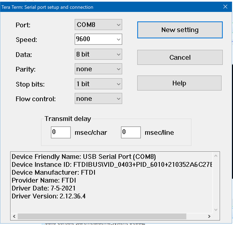
Use a Serial Terminal program to see the UART output. Here using Tera Term.
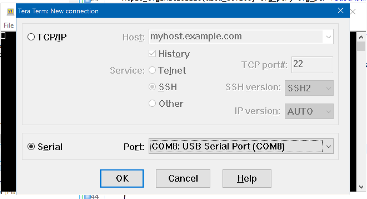
Choose 9600 bauds speed.
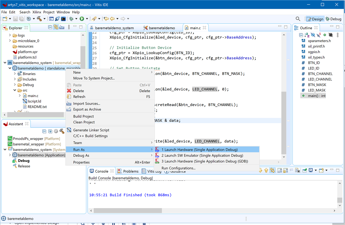
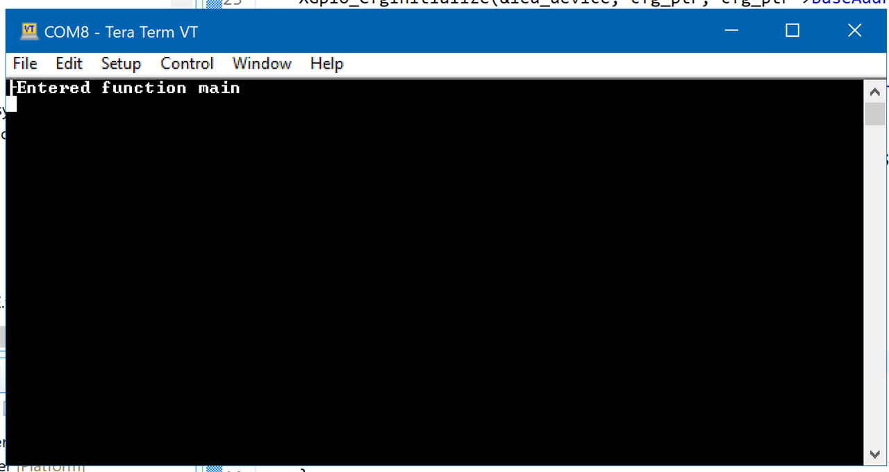
When the program starts it sends text through the UART
xil_printf("Entered function main\r\n");
This is all. Pressing each of the four buttons turns on the led of the same index.


Top Comments
-

Andrew J
-
Cancel
-
Vote Up
0
Vote Down
-
-
Sign in to reply
-
More
-
Cancel
Comment-

Andrew J
-
Cancel
-
Vote Up
0
Vote Down
-
-
Sign in to reply
-
More
-
Cancel
Children