element14 Community
element14 Community
    Register Log In
  • Site
  • Search
  • Log In Register
  • Community Hub
    Community Hub
    • What's New on element14
    • Feedback and Support
    • Benefits of Membership
    • Personal Blogs
    • Members Area
    • Achievement Levels
  • Learn
    Learn
    • Ask an Expert
    • eBooks
    • element14 presents
    • Learning Center
    • Tech Spotlight
    • STEM Academy
    • Webinars, Training and Events
    • Learning Groups
  • Technologies
    Technologies
    • 3D Printing
    • FPGA
    • Industrial Automation
    • Internet of Things
    • Power & Energy
    • Sensors
    • Technology Groups
  • Challenges & Projects
    Challenges & Projects
    • Design Challenges
    • element14 presents Projects
    • Project14
    • Arduino Projects
    • Raspberry Pi Projects
    • Project Groups
  • Products
    Products
    • Arduino
    • Avnet Boards Community
    • Dev Tools
    • Manufacturers
    • Multicomp Pro
    • Product Groups
    • Raspberry Pi
    • RoadTests & Reviews
  • Store
    Store
    • Visit Your Store
    • Choose another store...
      • Europe
      •  Austria (German)
      •  Belgium (Dutch, French)
      •  Bulgaria (Bulgarian)
      •  Czech Republic (Czech)
      •  Denmark (Danish)
      •  Estonia (Estonian)
      •  Finland (Finnish)
      •  France (French)
      •  Germany (German)
      •  Hungary (Hungarian)
      •  Ireland
      •  Israel
      •  Italy (Italian)
      •  Latvia (Latvian)
      •  
      •  Lithuania (Lithuanian)
      •  Netherlands (Dutch)
      •  Norway (Norwegian)
      •  Poland (Polish)
      •  Portugal (Portuguese)
      •  Romania (Romanian)
      •  Russia (Russian)
      •  Slovakia (Slovak)
      •  Slovenia (Slovenian)
      •  Spain (Spanish)
      •  Sweden (Swedish)
      •  Switzerland(German, French)
      •  Turkey (Turkish)
      •  United Kingdom
      • Asia Pacific
      •  Australia
      •  China
      •  Hong Kong
      •  India
      •  Korea (Korean)
      •  Malaysia
      •  New Zealand
      •  Philippines
      •  Singapore
      •  Taiwan
      •  Thailand (Thai)
      • Americas
      •  Brazil (Portuguese)
      •  Canada
      •  Mexico (Spanish)
      •  United States
      Can't find the country/region you're looking for? Visit our export site or find a local distributor.
  • Translate
  • Profile
  • Settings
Embedded and Microcontrollers
  • Technologies
  • More
Embedded and Microcontrollers
Blog Renesas RX65 Envision Kit - part 8: DMA
  • Blog
  • Forum
  • Documents
  • Quiz
  • Polls
  • Files
  • Members
  • Mentions
  • Sub-Groups
  • Tags
  • More
  • Cancel
  • New
Join Embedded and Microcontrollers to participate - click to join for free!
  • Share
  • More
  • Cancel
Group Actions
  • Group RSS
  • More
  • Cancel
Engagement
  • Author Author: Jan Cumps
  • Date Created: 7 Dec 2019 12:39 PM Date Created
  • Views 2247 views
  • Likes 5 likes
  • Comments 6 comments
  • rt
  • renesas
  • dma
  • road_test
  • adc
Related
Recommended

Renesas RX65 Envision Kit - part 8: DMA

Jan Cumps
Jan Cumps
7 Dec 2019

I'm evaluating the Renesas RX65N MCU EV Kit.

In this post: A Direct Memory Access example.

image

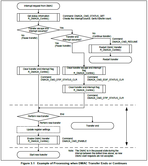
source: application  note R01AN2063EJ0220 DMAC Module Using Firmware Integration Technology


The Example - DMA and ADC


The Renesas DMA example is something you can use in the real world:

One of the ADC pins is sampled 32 times and the data is put into RAM by the DMA controller, without loading the microcontroller.

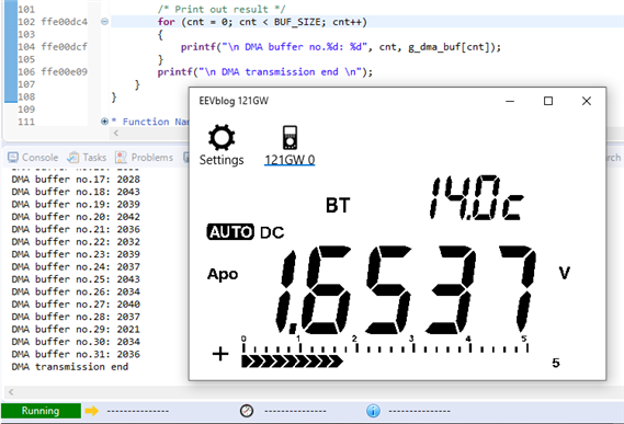
When all data is available and transferred, the firmware logs it to the debug console.
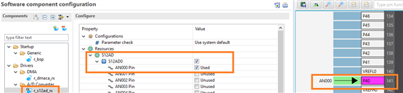
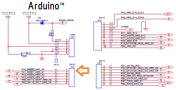
 

Pin Assignment


The analog input A000 is used. It's broken out on the Envision board to the Arduino connector CN10, pin 1.

image


image


The voltage at this pin will be sampled by the application. That voltage is made tapping off the wiper of  a 10K potentiometer.

image

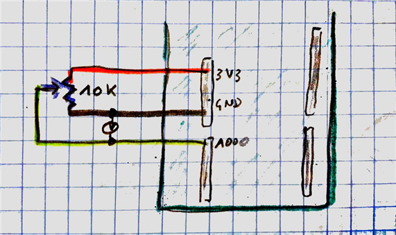
For reference, I've connected a voltmeter to the wiper.


image


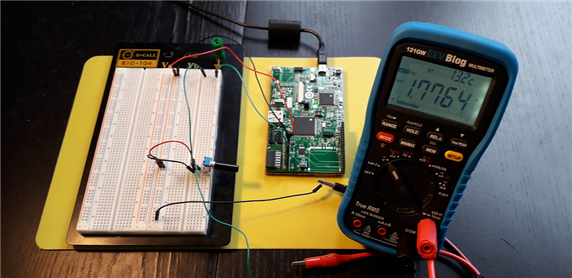
The result is that the log shows a number between 0 and 4095, where 0 is 0V and 4095 represents 3.3V.

The potentiometer can be used to swipe between the two values.

image


Firmware


DMA init


The DMA channel used is channel 1 (DMACA_CH1), and the source is - as expected - ADC input 0 (IR_S12ADC0_S12ADI0).


dmaca_return_t dma_init(void)
{
    dmaca_return_t ret = DMACA_SUCCESS;
    dmaca_stat_t p_stat_dmaca;

    /* Open DMA module */
    R_DMACA_Init();
    ret = R_DMACA_Open(DMACA_CH1);
    if (DMACA_SUCCESS == ret)
    {
        /* Initial DMA */
        g_dma_cfg.act_source            = IR_S12ADC0_S12ADI0;
        g_dma_cfg.request_source        = DMACA_TRANSFER_REQUEST_PERIPHERAL;
        g_dma_cfg.transfer_mode         = DMACA_TRANSFER_MODE_REPEAT;
        g_dma_cfg.data_size             = DMACA_DATA_SIZE_WORD;
        g_dma_cfg.src_addr_mode         = DMACA_SRC_ADDR_FIXED;
        g_dma_cfg.src_addr_repeat_area  = DMACA_SRC_ADDR_EXT_REP_AREA_NONE;
        g_dma_cfg.des_addr_mode         = DMACA_DES_ADDR_INCR;
        g_dma_cfg.des_addr_repeat_area  = DMACA_DES_ADDR_EXT_REP_AREA_NONE;
        g_dma_cfg.repeat_block_side     = DMACA_REPEAT_BLOCK_DESTINATION;
        g_dma_cfg.interrupt_sel         = DMACA_CLEAR_INTERRUPT_FLAG_BEGINNING_TRANSFER;
        g_dma_cfg.dtie_request          = DMACA_TRANSFER_END_INTERRUPT_ENABLE;
        g_dma_cfg.esie_request          = DMACA_TRANSFER_ESCAPE_END_INTERRUPT_DISABLE;
        g_dma_cfg.rptie_request         = DMACA_REPEAT_SIZE_END_INTERRUPT_DISABLE;
        g_dma_cfg.sarie_request         = DMACA_SRC_ADDR_EXT_REP_AREA_OVER_INTERRUPT_DISABLE;
        g_dma_cfg.darie_request         = DMACA_DES_ADDR_EXT_REP_AREA_OVER_INTERRUPT_DISABLE;
        g_dma_cfg.p_src_addr            = (void *)&S12AD.ADDR0;
        g_dma_cfg.p_des_addr            = (void *)&g_dma_buf;
        g_dma_cfg.offset_value          = 0;
        g_dma_cfg.transfer_count        = 1;
        g_dma_cfg.block_size            = BUF_SIZE;
        ret = R_DMACA_Control(DMACA_CH1, DMACA_CMD_ALL_ENABLE, &p_stat_dmaca);
    }

    return ret;
}


ADC init


adc_err_t adc_init(void)
{
    adc_err_t ret = ADC_SUCCESS;
    adc_cfg_t adc_cfg;
    adc_ch_cfg_t ch_cfg;

    adc_cfg.resolution = ADC_RESOLUTION_12_BIT;
    adc_cfg.alignment = ADC_ALIGN_RIGHT;
    adc_cfg.add_cnt = ADC_ADD_OFF;
    adc_cfg.clearing = ADC_CLEAR_AFTER_READ_OFF;
    adc_cfg.trigger = ADC_TRIG_SYNC_TRG0AN;
    adc_cfg.trigger_groupb = ADC_TRIG_NONE;
    adc_cfg.priority = 3;
    adc_cfg.priority_groupb = 0;
    adc_cfg.temp_sensor = ADC_TEMP_SENSOR_NOT_AD_CONVERTED;
    adc_cfg.add_temp_sensor = ADC_TEMP_SENSOR_ADD_OFF;

    ret = R_ADC_Open(0, ADC_MODE_SS_ONE_CH, &adc_cfg, adc_callback);
    R_ADC_PinSet_S12AD0();

    ch_cfg.chan_mask = ADC_MASK_CH0;                     // select channel 0 (POT)
    ch_cfg.priority_groupa = ADC_GRPA_PRIORITY_OFF;      // group mode not used
    ch_cfg.chan_mask_groupb = ADC_MASK_GROUPB_OFF;       // group mode not used
    ch_cfg.chan_mask_groupc = ADC_MASK_GROUPC_OFF;       // group mode not used
    ch_cfg.add_mask = ADC_MASK_ADD_OFF;                  // no channels using addition
    ch_cfg.diag_method = ADC_DIAG_OFF;                   // self-diagnosis off
    ch_cfg.anex_enable = false;                          // no external amplifier
    ch_cfg.sample_hold_mask = ADC_MASK_SAMPLE_HOLD_OFF;  // Bypass chnl-dedicated S&H circuits
    ch_cfg.sample_hold_states = ADC_SST_SH_CNT_DEFAULT;  // default sample & hold states

    if (ADC_SUCCESS == ret)
    {
        R_ADC_Control(0, ADC_CMD_ENABLE_CHANS, &ch_cfg);
        init_mtu0();
    }
    if (ADC_SUCCESS == ret)
    {
        R_ADC_Control(0, ADC_CMD_ENABLE_TRIG, FIT_NO_PTR);
    }

    return ret;
}


The Multi-Function Timer Pulse Unit is used to wait after the ADC channel is enabled (line 34). The code is available in the example and a nice example on how to create a wait without a while(nothing) loop.


An ADC callback function is mandatory in an interrupt driven design. In this case, where the info is transferred via the DMA, the callback doesn't have to do anything.

Hence this code:


void adc_callback(void *pArgs)
{
    nop();
}


DMA start


The DMA is kicked off in this function:

First, channel 0 is disabled (line 6), then configured line 9).

After that it's activated (line 13).


dmaca_return_t dma_start(void)
{
    dmaca_return_t ret = DMACA_SUCCESS;
    dmaca_stat_t p_stat_dmaca;

    ret = R_DMACA_Control(DMACA_CH1, DMACA_CMD_DISABLE, &p_stat_dmaca);
    if (DMACA_SUCCESS == ret)
    {
        ret = R_DMACA_Create(DMACA_CH1, &g_dma_cfg);
    }
    if (DMACA_SUCCESS == ret)
    {
        ret = R_DMACA_Control(DMACA_CH1, DMACA_CMD_ENABLE, &p_stat_dmaca);
    }

    return ret;
}


Main program


The main program, as usual, initialised buffers and variables, then sets the DMA mechanism in motion.

You'll see how the functions documented above work together.


Each loop, DMA is started, then the RX65 waits for the sampling and transfer to complete.

You can do something else than waiting here. The processor is free because DMA works autonomous.

Once the cycle is finished, the results are logged.

Repeat.


#define BUF_SIZE      (32)                            /* Buffer size */
// ...
static uint16_t g_dma_buf[BUF_SIZE];                  /* Reception buffer */
dmaca_transfer_data_cfg_t g_dma_cfg;

void main(void)
{
    static uint8_t cnt;
    static uint8_t rcpflag;
    dmaca_stat_t p_stat_dmaca;

    /* Initial configurations */
    R_Systeminit();
    dma_init();
    adc_init();

    /* Main routine */
    while (1)
    {
        /* Reset DMA buffer */
        for (cnt = 0; cnt < BUF_SIZE; cnt++)
        {
            g_dma_buf[cnt] = 0;
        }

        /* Start DMA transfer */
        dma_start();

        /* Wait routine for the completion of DMA transfer (CPU can run other task instead) */
        rcpflag = 0;
        while (rcpflag == 0)
        {
            R_DMACA_Control(DMACA_CH1, DMACA_CMD_STATUS_GET, &p_stat_dmaca);
            if ((true == p_stat_dmaca.dtif_stat) && (0 == p_stat_dmaca.transfer_count))
            {
                rcpflag = 1;
            }
        }

        /* Print out result */
        for (cnt = 0; cnt < BUF_SIZE; cnt++)
        {
            printf("\n DMA buffer no.%d: %d", cnt, g_dma_buf[cnt]);
        }
        printf("\n DMA transmission end \n");
    }
}


All code displayed here is from the application note R01AN2063EJ0220 DMAC Module Using Firmware Integration Technology's example, without changes. In this case I can publish selected snippets as fair use - comment upon.

/***********************************************************************************************************************
* DISCLAIMER
* This software is supplied by Renesas Electronics Corporation and is only intended for use with Renesas products. No
* other uses are authorized. This software is owned by Renesas Electronics Corporation and is protected under all
* applicable laws, including copyright laws.
* THIS SOFTWARE IS PROVIDED "AS IS" AND RENESAS MAKES NO WARRANTIES REGARDING
* THIS SOFTWARE, WHETHER EXPRESS, IMPLIED OR STATUTORY, INCLUDING BUT NOT LIMITED TO WARRANTIES OF MERCHANTABILITY,
* FITNESS FOR A PARTICULAR PURPOSE AND NON-INFRINGEMENT. ALL SUCH WARRANTIES ARE EXPRESSLY DISCLAIMED. TO THE MAXIMUM
* EXTENT PERMITTED NOT PROHIBITED BY LAW, NEITHER RENESAS ELECTRONICS CORPORATION NOR ANY OF ITS AFFILIATED COMPANIES
* SHALL BE LIABLE FOR ANY DIRECT, INDIRECT, SPECIAL, INCIDENTAL OR CONSEQUENTIAL DAMAGES FOR ANY REASON RELATED TO THIS
* SOFTWARE, EVEN IF RENESAS OR ITS AFFILIATES HAVE BEEN ADVISED OF THE POSSIBILITY OF SUCH DAMAGES.
* Renesas reserves the right, without notice, to make changes to this software and to discontinue the availability of
* this software. By using this software, you agree to the additional terms and conditions found by accessing the
* following link:
* http://www.renesas.com/disclaimer
*
* Copyright (C) 2019 Renesas Electronics Corporation. All rights reserved.
***********************************************************************************************************************/


Related blog
part 1: Create an Empty Project
part 2a: Blinky with GCC Toolchain
part 2b: Blinky with Timer and Interrupt
part 3: Port an example from Renesas toolchain to GCC
part 4a: Low Power - Sleep
part 4b: Low Power - Software Standby
4c todo: power mode 3
4d todo: power mode 4
part 5: DAC
part 6: Software SHA
part 7: Blinky with FreeRTOS
part 8: DMA
part 9: UART
part 10: Reserve LCD Frame Buffer in Expansion RAM with GCC
part 11: port emWIN to GCC and run an LCD Widget
Renesas RX65N MCU EV Kit - Review
Andrew Johnson's blog series
Renesas Envision Kit RPBRX65N Roadtest
  • Sign in to reply

Top Comments

  • Andrew J
    Andrew J over 5 years ago +2
    This was going to be my next activity with the board, once my headers arrive (next day delivery seems to have a different definition in CPC.Farnell's world!) so it's good to see. I'll trade you the base…
  • Jan Cumps
    Jan Cumps over 5 years ago in reply to Andrew J +1
    It's the unchanged example from Renesas: https://www.renesas.com/eu/en/software/D4800134.html . Not a single line altered (that's why I put the "fair use:comment upon" part in the blog. It's not my code…
  • Jan Cumps
    Jan Cumps over 5 years ago +1
    ... looking at the serial comms peripherals at the moment It's the first time I run against limits of the debug port. It can be used for debugging OR serial comms. Most debuggers manage to have dual use…
  • Andrew J
    Andrew J over 5 years ago in reply to Jan Cumps

    The same type of people who say use vi and the command line, anything else slows you down and gets in the way.

    • Cancel
    • Vote Up +1 Vote Down
    • Sign in to reply
    • More
    • Cancel
  • Jan Cumps
    Jan Cumps over 5 years ago in reply to Andrew J

    You can, but you have to put the dip-switch SW1 and SW4 in such a position that it's either-or.

    I could not get serial over USB working and be able to debug the device.


    That's why I'm currently using the serial port 9 that's broken out to the PMOD connector. I can debug and see characters arriving and leaving.

    Later on switching to SCI#5  - the one linked to the USB debug port - once the code is working is straightforward.


    Many people say that using a debugger is a sign that you don't know what you're doing. For me it's an integral part of the develop -> Test cycle. I use the debugger a lot.

    • Cancel
    • Vote Up +1 Vote Down
    • Sign in to reply
    • More
    • Cancel
  • Andrew J
    Andrew J over 5 years ago in reply to Jan Cumps

    Can you not use the USB-A port for serial comms - that's what I was expecting?

    • Cancel
    • Vote Up 0 Vote Down
    • Sign in to reply
    • More
    • Cancel
  • Jan Cumps
    Jan Cumps over 5 years ago

    ... looking at the serial comms peripherals at the moment


    image


    It's the first time I run against limits of the debug port. It can be used for debugging OR serial comms. Most debuggers manage to have dual use in parallel.

    I'm using a TI launchpad as the USB to 3V3 translator to bypass this..


    image

    • Cancel
    • Vote Up +1 Vote Down
    • Sign in to reply
    • More
    • Cancel
  • Jan Cumps
    Jan Cumps over 5 years ago in reply to Andrew J

    It's the unchanged example from Renesas: https://www.renesas.com/eu/en/software/D4800134.html . Not a single line altered (that's why I put the "fair use:comment upon" part in the blog. It's not my code I post here).


    I'm procrastinating on the LCD development.Secretly hoping that it 'll be the focus of another reviewer (you image ) and that the road test reviews and blogs are complementary.

    • Cancel
    • Vote Up +1 Vote Down
    • Sign in to reply
    • More
    • Cancel
>
element14 Community

element14 is the first online community specifically for engineers. Connect with your peers and get expert answers to your questions.

  • Members
  • Learn
  • Technologies
  • Challenges & Projects
  • Products
  • Store
  • About Us
  • Feedback & Support
  • FAQs
  • Terms of Use
  • Privacy Policy
  • Legal and Copyright Notices
  • Sitemap
  • Cookies

An Avnet Company © 2025 Premier Farnell Limited. All Rights Reserved.

Premier Farnell Ltd, registered in England and Wales (no 00876412), registered office: Farnell House, Forge Lane, Leeds LS12 2NE.

ICP 备案号 10220084.

Follow element14

  • X
  • Facebook
  • linkedin
  • YouTube