


I am learning SystemVerilog HDL. I started reading the book FPGA Prototyping By SystemVerilog Examples. These are my study notes and what I am learning about SystemVerilog. My idea is to do exercises with the Digilent Arty S7 50 board obtained in the "7 ways to leave your Spartan 6" program. I don't have a set plan and will post new notes as I have time to expand my knowledge. These notes assume that you already know how to use the Vivado tools to build and load a hardware-only design. If not, I've prepared a tutorial on how to do it: Arty S7 50 First Baremetal Software Project
Table of Contents
Chapters:
- Gate-Level Combinational Circuit
- RTL Combinational Circuit Operators
- RTL Combinational Circuit - Concurrent and Control Constructs
- Hex-Digit to Seven-Segment LED Decoder RTL Combinational Circuit
- Barrel Shifter RTL Combinational Circuit
- Simplified Floating Point Arithmetic. RTL Combinational Circuit
- BCD Number Format. RTL Combinational Circuit
- DDFS. Direct Digital Frequency Synthesis for Sound
- FPGA ADSR envelope generator for sound synthesis
- AMD Xilinx 7 series FPGAs XADC
- Building FPGA-Based Music Instrument Synthesis: A Simple Test Bench Solution
SystemVerilog

SystemVerilog is one of the major HDLs. HDL stands for Hardware Description Language. HDL is used to describe and model digital systems.
SystemVerilog, standardized as IEEE 1800, is a hardware description and hardware verification language used to model, design, simulate, test and implement electronic systems. Verilog was developed for gate-level and register-transfer-level design and modeling without the inclusion of advanced high-level verification features. SystemVerilog is a hardware description and verification language.
You can download the standard for free from: 1800-2017 - IEEE Standard for SystemVerilog--Unified Hardware Design, Specification, and Verification Language | IEEE Standard | IEEE Xplore through the IEEE GET Program TM
"IEEE Standard for SystemVerilog--Unified Hardware Design, Specification, and Verification Language," in IEEE Std 1800-2017 (Revision of IEEE Std 1800-2012) , vol., no., pp.1-1315, 22 Feb. 2018, doi: 10.1109/IEEESTD.2018.8299595.
Gate-Level Combinational Circuit
In this blog we will discuss Gate-Level Combinational Circuits. A Gate-Level Combinational Circuit is composed of simple logic gates like a simple comparator.
Simple SystemVerilog program
To see what the skeleton of a SystemVerilog program looks like, we are going to build a simple 1-bit comparator.
1-bit equality comparator with two inputs, a and b, and an output eq. eq signal is asserted when a and b are equal

Truth table of 1-bit equality comparator
|
Input |
Output |
|
| a | b | eq |
| 0 | 0 | 1 |
| 0 | 1 | 0 |
| 1 | 0 | 0 |
| 1 | 1 | 1 |
Using basic logic gates we can describe the circuit as a sum-of-products
eq = a. b + a' . b'
One possible implementation in SystemVerilog
module eq1(
    input logic a,
    input logic b,
    output logic eq
    );

  // signal declaration
  logic p0, p1;

  // body
  // sum of product terms
  assign eq = p0 | p1;
  // product terms
  assign p0 = ~a & ~b;
  assign p1 = a & b;

endmodule
The order of the continuous statements is irrelevant and can be rearranged arbitrarily.
This is the Vivado elaborated design

We could have described the circuit using ^ (xor) and ~ (not) bitwise operators.
eq = ~ ( a ^ b )
One possible implementation in Verilog
module eq1_xor(
    input a,
    input b,
    output eq
    );

    assign eq = ~(a ^ b);

endmodule
And the Vivado elaborated design:

Lexical Elements
- Identifier: Gives an unique name to an object: eq, a, b. Is composed of letters, digits, underscore character (_) and the dollar sign ($). The first character must be a letter or underscore. System Verilog is case-sensitive.
- Keyword: Is a predefined identifier used to describe language constructs.
- White space: This includes the space, tab, and new line characters is used to separate identifiers. Can be uses freely.
- Comments: Is just for documentation and it is ignored by software. A one-line comment starts with // . A multiple-line comment is encapsulated between /* and */
Data types
SystemVerilog supports a rich collection of data types. The following set allows defining a wide variety of circuits:
- logic type
- integer type
- tri type
- user-defined enumerate type
Logic type represents the value of a one bit signal. The logic type can assume a value from four-state set:
- 0: logic 0 or a false condition
- 1: logic 1 or a true condition
- z: high-impedance state. Output of a tristate buffer
- x: unknown value. Used as a value that is not 0, 1, or z, as an uninitialized input or output conflict.
A collection of signals can be grouped into a bus, or a collection of data bits can be grouped into a word. It can be represented using a one-dimensional array or vector.
logic [7:0] data1, data2; // 8-bit data
logic [31:0] addr; // 32-bit address
logic [0:7] reverse_data; // index reversed
Index range can be descending [7:0] or ascending [0:7]. Descending is preferred since the leftmost position corresponds to the MSB (most significant bit) of a binary number.
Two dimensional arrays can be defined as
logic [31:0] mem [0:3]; // 4 x 32 memory
Integer type is a special case of one-dimensional logic array. Its size is fixed at 32 bits and it is interpreted as a signed binary number.
Number representation
The value of a one-dimensional logic array is represented as a constant number.
General format:
[sign][size]'[base][value]
[base] specifies the base of the number, can be:
- b or B: binary
- o or O: octal
- h or H: hexadecimal
- d or D: decimal
[size] Optional. Number of bits in a number
[value] the value of the number in the corresponding [base]. Underline character can be included for clarity
| Number | Stored Value | Comment |
| 5'b11010 | 11010 | binary |
| 5'b11_010 | 11010 | _ ignored |
| 5'o32 | 11010 | octal |
| 5'h1a | 11010 | hexadecimal |
| 5d26 | 11010 | decimal |
| 5'b0 | 00000 | 0 extended |
| 5'b1 | 00001 | 0 extended |
| 5'bz | zzzzz | z extended |
| 5'bx | xxxxx | x extended |
| 5'bx01 | xxx01 | x extended |
| -5'00001 | 11111 | 2's complement of 00001 |
| 'b11010 | 00000000 00000000 00000000 00011010 | extended to 32 bits |
| 'hee | 00000000 00000000 00000000 11101110 | extended to 32 bits |
| 1 | 00000000 000000 00 00000000 00000001 | extended to 32 bits |
| -1 | 11111111 11111111 11111111 11111111 | extended to 32 bits |
Operators
SystemVerilog has several operators. In the example we have used bitwise operators like ~ (not), & (and), | (or), and ^ (xor). These operators infer basic gate-level cells.
HDL Program Skeleton
Most HDL codes follow a basic skeleton: I/O port declaration, signal declaration, and module body.

Port declaration: The I/O declaration specifies the modes, data types, and names of the module I/O ports.
The simplified syntax is:
module [module_name]
(
[mode] [data_type] [port_names],
[mode] [data_type] [port_names],
...
[mode] [data_type] [port_names],
);
- mode can be input, output, or inout
- logic type is used for the input and output ports and tri type for bidirectional ports
Signal declaration portion specifies the internal variables and local parameters used in the module. Variables frequently resemble the interconnecting wires between circuit parts.
The simplified syntax of signal declaration is
[data_type] [port_names];
An identifier does not need to be declared explicitly. If a declaration is omitted, the signal is assumed to be an implicit net.
The program body can be thought of a collection of circuit parts. A part can be described as:
- Continuous assignment as in
assign [signal_name] = [expression]; - "Always block": procedural assignments that can describe more complex circuit operation.
- Module instantiation: creates an instance of another module.
Concurrent semantics: The statements of an HDL program are "autonomous" and executed concurrently.
Structural description
SystemVerilog allows you to create a large system out of simpler or predefined components by using a mechanism called module instantiation.
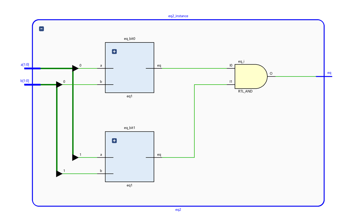
We are going to build a two-bit comparator using two blocks of 1-bit comparators. Gate-level implementation of a 2-bit comparator from 1-bit comparators.

module eq2(
    // I/O Ports
    input logic [1:0] a,
    input logic [1:0] b,
    output logic eq
    );

  // signal declaration
  logic e0,e1;

  // body
  // instantiate two 1-bit comparators
  eq1 eq_bit0(.a(a[0]), .b(b[0]), .eq(e0));
  eq1 eq_bit1(.a(a[1]), .b(b[1]), .eq(e1));

  // a and b are equal if individual bits are equal
  assign eq = e0 & e1;

endmodule
Vivado elaborated design:
The module code includes two module instantiation statements. The simplified syntax of module instantiation is
[module_name] [instance_name]
(
.[port_name]([signal_name]),
.[port_name]([signal_name]),
...
);
- module_name: indicates the name of the module to instantiate. eq1
- instance_name: gives a unique id for an instance. eq_bit0
- Port connection: indicates the connections between I/O ports of the instantiated module and the external signals used in the current module. .a(a[0])
If the port names and signals names are identical this can be represented as ".*" in SystemVerilog:
eq1 eq_bit0(.a(a), .b(b), .eq(eq));
can be abbreviated as
eq1 eq_bit0(.*);
and the instantiation statement
eq1 eq_bit0(.a(a), .b(b), .eq(result));
can be abbreviated as
eq1 eq_bit0(.*, .eq(result));
This format of mapping the ports is known as connection by name. An alternative scheme is connection by ordered list or connection by position. The port names of the lower-level module are omitted and the signals of the higher-level module are listed in the same order as the lower module's port declaration.
eq1 eq_bit0(a, b, result);
This scheme is more compact but it is error prone.
Module Wrapper. Top-Level Signal Mapping
We are going to use the Digilent Arty S7 50 prototyping board. When an HDL program is intended for a particular physical device, the design is subject to several constraints. One of the constraints is the location of the I/O pins.
For example the switches and LEDs on the board are pre-wired to specific pins on the FPGA device and cannot be altered. The pin assignment is defined in a constraints file that is processed together with the HDL files.
We will use the constraints file that Digilent provides for their Arty S7 50 board. You can download it from:
https://github.com/Digilent/digilent-xdc/blob/master/Arty-S7-50-Master.xdc
To use this file, the top-level HDL module must have the same predefines I/O signals names. This can be achieved by creating an HDL file to "warp" the original design and map its original I/O signals to the prototyping board's I/O signals.
Top-level wrapping circuit
module eq2_wrapper(
    input [3:0] sw,
    output [0:0] led
    );

    eq2 eq2_instance(.a(sw[3:2]),.b(sw[1:0]),.eq( led[0]));
endmodule
The code maps the logical port names of the comparator to the physical signals on the prototyping board.
We name the I/O pins connected to the slide switches and LEDs as sw and led and specify their pin assignment in the constraint file
Constraint file
## Switches
set_property -dict { PACKAGE_PIN H14   IOSTANDARD LVCMOS33 } [get_ports { sw[0] }]; #IO_L20N_T3_A19_15 Sch=sw[0]
set_property -dict { PACKAGE_PIN H18   IOSTANDARD LVCMOS33 } [get_ports { sw[1] }]; #IO_L21P_T3_DQS_15 Sch=sw[1]
set_property -dict { PACKAGE_PIN G18   IOSTANDARD LVCMOS33 } [get_ports { sw[2] }]; #IO_L21N_T3_DQS_A18_15 Sch=sw[2]
set_property -dict { PACKAGE_PIN M5    IOSTANDARD SSTL135 } [get_ports { sw[3] }]; #IO_L6N_T0_VREF_34 Sch=sw[3]

## LEDs
set_property -dict { PACKAGE_PIN E18   IOSTANDARD LVCMOS33 } [get_ports { led[0] }]; #IO_L16N_T2_A27_15 Sch=led[2]
The 2-bit comparator on the Digilent Arty S7 50 board.
Vivado elaborated design of the wrapper. High-level view

Elaborated schematic by Vivado

Vivado project sources hierarchy

Test-bench
A test-bench will allow us to verify the functionality of a design through simulations. After the code is developed, it can be simulated in a host computer to verify the correctness of the circuit operation and the synthesized to a physical device.
A test-bench is a container where the design is placed and driven with different stimulus.
Test bench for the 1-bit comparator
// test bench for the 1 bit comparator

module eq1_testbench;

  // signal declaration
  logic test_a, test_b;
  logic test_eq;

  // instantiate the circuit under test
  eq1 uut(.a(test_a), .b(test_b), .eq(test_eq));

  // test vector generator
  initial
    begin

      // test vector 1
      test_a = 1'b0;
      test_b = 1'b0;
      #200;

      // test vector 2
      test_a = 1'b1;
      test_b = 1'b0;
      #200;

      // test vector 3
      test_a = 1'b0;
      test_b = 1'b1;
      #200;

      // test vector 1
      test_a = 1'b1;
      test_b = 1'b1;
      #200;

      $stop
    end

endmodule
The code consists of a module instantiation statement, which creates an instance of the 1-bit comparator, and an initial block, which generates a sequence of test patterns.
The initial block is a special language construct, which is executed once when the simulation starts. The statements inside an initial block are executed sequentially
Each test pattern is generated by three statements:
 // test vector 2
 test_a = 1'b1;
 test_b = 1'b0;
 #200;
The first two statements specify the values for the test_a and test_b signals, and the third indicates that the two values will last for 200 time units.
The last statement, $stop, is a system function that stops the simulation and return the control to simulation software.
Vivado Simulation

Same result for the xnor version:
module eq1_xor_testbench;

  // signal declaration
  logic test_a, test_b;
  logic test_eq;

  // instantiate the circuit under test
  eq1_xor uut(.a(test_a), .b(test_b), .eq(test_eq));

  // test vector generator
  initial
    begin
          // Dump waves
    $dumpfile("dump.vcd");
    $dumpvars(1);


      // test vector 1
      test_a = 1'b0;
      test_b = 1'b0;
      #200;
      // test vector 2
      test_a = 1'b1;
      test_b = 1'b0;
      #200;
      // test vector 3
      test_a = 1'b0;
      test_b = 1'b1;
      #200;
      // test vector 1
      test_a = 1'b1;
      test_b = 1'b1;
      #200;
      $stop;
    end


  task display;
    #1 $display("i0:%0h, i1:%0h, eq:%0h",
      test_a, test_b, test_eq);
  endtask

endmodule

Test bench for the 2-bit comparator
`timescale 1ns / 10ps

// 2-bit comparator module techbench
module eq2_testbench;

  // signal declaration
  logic [1:0] test_a, test_b;
  logic test_eq;

  // instantiate the circuit under test
  eq2 uut(.a(test_a), .b(test_b), .eq(test_eq));

  // test vector generator
  initial
    begin
      // Dump waves
     // $dumpfile("dump.vcd");
    //  $dumpvars(1);

      // test vector 1
      test_a = 2'b00;
      test_b = 2'b00;
      #200;
      // test vector 2
      test_a = 2'b01;
      test_b = 2'b00;
      #200;
      // test vector 3
      test_a = 2'b10;
      test_b = 2'b00;
      #200;
      // test vector 4
      test_a = 2'b11;
      test_b = 2'b00;
      #200;

      // test vector 5
      test_a = 2'b00;
      test_b = 2'b01;
      #200;
      // test vector 6
      test_a = 2'b01;
      test_b = 2'b01;
      #200;
      // test vector 7
      test_a = 2'b10;
      test_b = 2'b01;
      #200;
      // test vector 8
      test_a = 2'b11;
      test_b = 2'b01;
      #200;

      // test vector 9
      test_a = 2'b00;
      test_b = 2'b10;
      #200;
      // test vector 10
      test_a = 2'b01;
      test_b = 2'b10;
      #200;
      // test vector 11
      test_a = 2'b10;
      test_b = 2'b10;
      #200;
      // test vector 12
      test_a = 2'b11;
      test_b = 2'b10;
      #200;

      // test vector 13
      test_a = 2'b00;
      test_b = 2'b11;
      #200;
      // test vector 14
      test_a = 2'b01;
      test_b = 2'b11;
      #200;
      // test vector 15
      test_a = 2'b10;
      test_b = 2'b11;
      #200;
      // test vector 16
      test_a = 2'b11;
      test_b = 2'b11;
      #200;

      $stop;

    end
endmodule
Vivado Simulation:

SystemVerilog Programming Exercises
Gate-level greater-than circuit
We are going to develop a new exercise with only only gate-level logical operators, a greater-than circuit.
The greater-than circuit compares two inputs, a and b, and asserts an output when a is greater than b. We want to create a 2-bit greater-than circuit from the bottom up and use only gate-level logical operators
Truth table for a 2-bit greater-than circuit

Karnaugh Map

Logic expression in the sum-of-products format
(A>B) = A1.B1’ + A0.B1’.B0’ + A1.A0.B0’
HDL code using only logical operators.
module gt2(
    input logic [1:0] a,
    input logic [1:0] b,
    output logic eq
    );

    logic p0;
    logic p1;
    logic p2;

    assign eq = p0 | p1 | p2;

    assign p0 = a[0] & (~ b[1]) & (~ b[0]);
    assign p1 = a[1] & (~b[1]);
    assign p2 = a[1] & a[0] & (~b[0]);

endmodule
Test bench for the 2-bit greater-than circuit.
`timescale 1ns / 1ps

module gt2_testbench();


  // signal declaration
  logic [1:0] test_a, test_b;
  logic test_eq;

  // instantiate the circuit under test
  gt2 uut(.a(test_a), .b(test_b), .eq(test_eq));

  // test vector generator
  initial
    begin

      // test vector 1
      test_a = 2'b00;
      test_b = 2'b00;
      #200;
      // test vector 2
      test_a = 2'b01;
      test_b = 2'b00;
      #200;
      // test vector 3
      test_a = 2'b10;
      test_b = 2'b00;
      #200;
      // test vector 4
      test_a = 2'b11;
      test_b = 2'b00;
      #200;

      // test vector 5
      test_a = 2'b00;
      test_b = 2'b01;
      #200;
      // test vector 6
      test_a = 2'b01;
      test_b = 2'b01;
      #200;
      // test vector 7
      test_a = 2'b10;
      test_b = 2'b01;
      #200;
      // test vector 8
      test_a = 2'b11;
      test_b = 2'b01;
      #200;

      // test vector 9
      test_a = 2'b00;
      test_b = 2'b10;
      #200;
      // test vector 10
      test_a = 2'b01;
      test_b = 2'b10;
      #200;
      // test vector 11
      test_a = 2'b10;
      test_b = 2'b10;
      #200;
      // test vector 12
      test_a = 2'b11;
      test_b = 2'b10;
      #200;

      // test vector 13
      test_a = 2'b00;
      test_b = 2'b11;
      #200;
      // test vector 14
      test_a = 2'b01;
      test_b = 2'b11;
      #200;
      // test vector 15
      test_a = 2'b10;
      test_b = 2'b11;
      #200;
      // test vector 16
      test_a = 2'b11;
      test_b = 2'b11;
      #200;

      $stop;

    end

endmodule
Perform a Simulation

Verify correctness
Whenever input signal A (2-bit unsigned integer) is greater than signal B eq is 1 otherwise 0.
Schematics generated by Vivado

Now we will use of the four switches as the inputs and one LED as the output.
Wrapper creation
`timescale 1ns / 1ps

module gt2_wrapper(
    input [3:0] sw,
    output [0:0] led
    );

    gt2 gt2_instance(.a(sw[3:2]),.b(sw[1:0]),.eq( led[0]));

endmodule
Again we configure the constraint file:
## Switchesset_property -dict { PACKAGE_PIN H14 IOSTANDARD LVCMOS33 } [get_ports { sw[0] }]; #IO_L20N_T3_A19_15 Sch=sw[0]set_property -dict { PACKAGE_PIN H18 IOSTANDARD LVCMOS33 } [get_ports { sw[1] }]; #IO_L21P_T3_DQS_15 Sch=sw[1]set_property -dict { PACKAGE_PIN G18 IOSTANDARD LVCMOS33 } [get_ports { sw[2] }]; #IO_L21N_T3_DQS_A18_15 Sch=sw[2]set_property -dict { PACKAGE_PIN M5 IOSTANDARD SSTL135 } [get_ports { sw[3] }]; #IO_L6N_T0_VREF_34 Sch=sw[3]
## LEDsset_property -dict { PACKAGE_PIN E18 IOSTANDARD LVCMOS33 } [get_ports { led[0] }]; #IO_L16N_T2_A27_15 Sch=led[2]
We can now synthesize the circuit and download the configuration file to the prototyping board. Check that everything works as expected.
Gate-level binary decoder
An n-to-2^n binary decoder asserts one of 2^n bits according to the input combination.

Logic expressions for the decoder:
bcode[0] = a[0]'.a[1]'.en
bcode[1] = a[0].a[1]'.en
bcode[2] = a[0]'.a[1].en
bcode[3] = a[0].a[1].en
SystemVerilog module
module encoder_2_to_4(
    input logic en,
    input logic [1:0] a,
    output logic [3:0] bcode
);
    assign bcode[0] = ~a[0] & ~a[1] & en;
    assign bcode[1] = a[0] & ~a[1] & en;
    assign bcode[2] = ~a[0] & a[1] & en;
    assign bcode[3] = a[0] & a[1] & en;

endmodule
SystemVerilog test bench
`timescale 1ns / 1ps

module encoder_2_to_4_testbench();

    // signal declaration
    logic en;
    logic [1:0] test_a;
    logic [3:0] test_bcode;

    // instantiate the circuit under test
    encoder_2_to_4 uut(.a(test_a), .en(en), .bcode(test_bcode));

    // test vector generator
    initial
    begin

        // test vector 1
        en = 1'b0;
        test_a = 2'b00;
        #200;

        // test vector 2
        en = 1'b0;
        test_a = 2'b01;
        #200;

        // test vector 3
        en = 1'b0;
        test_a = 2'b10;
        #200;

        // test vector 4
        en = 1'b0;
        test_a = 2'b11;
        #200;

        // test vector 1
        en = 1'b1;
        test_a = 2'b00;
        #200;

        // test vector 2
        en = 1'b1;
        test_a = 2'b01;
        #200;

        // test vector 3
        en = 1'b1;
        test_a = 2'b10;
        #200;

        // test vector 4
        en = 1'b1;
        test_a = 2'b11;
        #200;

        $stop;
    end

endmodule
Vivado Simulation

Wrapper creation
Use one switch as enable and two switches as input. Use the four LEDs as output.
`timescale 1ns / 1ps

module encoder_2_to_4_wrapper(
    input [3:0] sw,
    output [3:0] led
    );

    encoder_2_to_4 wrapper(.en(sw[2]), .a(sw[1:0]), .bcode(led));

endmodule
Vivado elaborated design. Schematic


Upload the configuration file to the board and play. We're done.

Conclusion
In this blog, we've done some simple gate-level combinational circuit programming exercises in SystemVerilog. These exercises can be done in many ways in SystemVerilog but we have done them this way to learn the basic structure of a SystemVerilog program and how to bench test our circuit.
SystemVerilog Study Notes Chapters
- Gate-Level Combinational Circuit
- RTL Combinational Circuit Operators
- RTL Combinational Circuit - Concurrent and Control Constructs
- Hex-Digit to Seven-Segment LED Decoder RTL Combinational Circuit
- Barrel Shifter RTL Combinational Circuit
- Simplified Floating Point Arithmetic. RTL Combinational Circuit
- BCD Number Format. RTL Combinational Circuit
- DDFS. Direct Digital Frequency Synthesis for Sound
- FPGA ADSR envelope generator for sound synthesis
- AMD Xilinx 7 series FPGAs XADC
- Building FPGA-Based Music Instrument Synthesis: A Simple Test Bench Solution
Top Comments