


RTL Combinational Circuit - Design Examples - Hex-Digit to Seven-Segment LED Decoder RTL Combinational Circuit
We have been reviewing the main constructs and operators for designing combinational logic circuits with the SystemVerilog HDL. Let's apply what we've learned by designing a combinational RTL hex-digit-to-seven-segment LED decoder circuit. To test it, we will design a small test circuit that will introduce us to the technique of Multi-Digit Seven-Segment LED Displays with Time Multiplexing.
Table of Contents
- Multi-Digit Seven-Segment LED Display Time-Multiplexing
- Hexadecimal Digit to Seven-Segment LED Decoder
- Testing the Hex-digit to Seven-Segment LED decoder with the Digilent Pmod SSD
- Driving Multi-Digit Seven-Segment LED Displays with Time-Multiplexing Scheme
- Multi-Digit Seven-Segment LED Display Time-Multiplexing Testing Circuit
- The LED display time-multiplexing test circuit in action
- SystemVerilog Study Notes Chapters
SystemVerilog Study Notes Chapters
- Gate-Level Combinational Circuit
- RTL Combinational Circuit Operators
- RTL Combinational Circuit - Concurrent and Control Constructs
- Hex-Digit to Seven-Segment LED Decoder RTL Combinational Circuit
- Barrel Shifter RTL Combinational Circuit
- Simplified Floating Point Arithmetic. RTL Combinational Circuit
- BCD Number Format. RTL Combinational Circuit
- DDFS. Direct Digital Frequency Synthesis for Sound
- FPGA ADSR envelope generator for sound synthesis
- AMD Xilinx 7 series FPGAs XADC
- Building FPGA-Based Music Instrument Synthesis: A Simple Test Bench Solution
Multi-Digit Seven-Segment LED Display Time-Multiplexing
Hexadecimal Digit to Seven-Segment LED Decoder
A hexadecimal digit to seven-segment LED decoder treats a 4-bit input as a hexadecimal digit and generates appropriate LEDs patterns
This is the sketch of a seven-segment LED display:
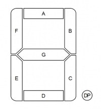
Seven-segment LED display and hexadecimal patterns


We can group together the LED control signals as g, f, e, d, c, b and a as a single 7-bit string. We suppose digits with a common cathode, so we need active high signals, then we can express the required patterns with the following bit strings:
0: 01111111: 00001102: 10110113: 10011114: 11001105: 11011016: 11111017: 00001118: 11111119: 1101111A: 1110111B: 1111100C: 1011000D: 1011110E: 1111001F: 1110001
SystemVerilog Hex-digit to Seven-Segment LED decoder implementation.
A possible implementation in SystemVerilog code for the hexadecimal digit to seven-segment LED decoder.
The code uses one selected signal assignment to list all the desired patterns for the seven LSBs of the sseg signal.
// hexadecimal digit to seven-segment LED decoder
// LED control signal g, f, e, d, c, b and a grouped as 7-bit signal sseg
// seven segment LED configured as active high
module hex_to_sseg(
    input logic [3:0] hex,
    output logic [6:0] sseg
);

    always_comb
    begin
        case (hex)
            4'h0: sseg[6:0] = 7'b0111111;
            4'h1: sseg[6:0] = 7'b0000110;
            4'h2: sseg[6:0] = 7'b1011011;
            4'h3: sseg[6:0] = 7'b1001111;
            4'h4: sseg[6:0] = 7'b1100110;
            4'h5: sseg[6:0] = 7'b1101101;
            4'h6: sseg[6:0] = 7'b1111101;
            4'h7: sseg[6:0] = 7'b0000111;
            4'h8: sseg[6:0] = 7'b1111111;
            4'h9: sseg[6:0] = 7'b1101111;
            4'hA: sseg[6:0] = 7'b1110111;
            4'hB: sseg[6:0] = 7'b1111100;
            4'hC: sseg[6:0] = 7'b1011000;
            4'hD: sseg[6:0] = 7'b1011110;
            4'hE: sseg[6:0] = 7'b1111001;
            default : sseg[6:0] = 7'b1110001; // 4'hF
        endcase

    end
endmodule
Hex-digit to Seven-Segment LED decoder test-bench
We can implement a simple test-bench to simulate all the possible hex digits values with a for-loop.
module hex_to_sseg_testbench;

    logic [3:0] hex;
    logic [6:0] sseg;

    hex_to_sseg uut(.*);

    initial
    begin
        for (int i = 0; i< 16; ++i)
        begin
            hex = i; #10;
        end
        $stop;
    end
endmodule
This is the Simulation test-bench scope view in Vivado:

Testing the Hex-digit to Seven-Segment LED decoder with the Digilent Pmod SSD
We will use the Digilent Pmod SSD . It is a 2 digit seven-segment display commonly used to display a counter or timer. The Pmod SSD utilizes a common cathode configuration to display a variety of LED segment combinations. This seven-segment LED is configured as active high, which means that an LED segment is lit if the corresponding control signal is '1'
The Pmod SSD communicates with the host board via the GPIO protocol. A logic level high signal on a particular anode will light up that respective segment on whichever digit is currently enabled. A particular digit can be selected by driving the Digit Selection pin (C) to a logic high or low voltage. Pmod SSD Reference Manual - Digilent Reference


Pmod SSD Pinout Description Table
| Header J1 | Header J2 | |||||
|---|---|---|---|---|---|---|
| Pin | Signal | Description | Pin | Signal | Description | |
| 1 | AA | Segment A | 1 | AE | Segment E | |
| 2 | AB | Segment B | 2 | AF | Segment F | |
| 3 | AC | Segment C | 3 | AG | Segment G | |
| 4 | AD | Segment D | 4 | C | Digit Selection pin | |
| 5 | GND | Power Supply Ground | 5 | GND | Power Supply Ground | |
| 6 | VCC | Positive Power Supply | 6 | VCC | Positive Power Supply | |
The PmodSSD does not have the dp LEDs connected to the Pmod connector.
Driving Multi-Digit Seven-Segment LED Displays with Time-Multiplexing Scheme
To save the number of I/O pins, a time-multiplexing scheme is sometimes used in multi-digit seven-segment LED display. In the case of the Pmod SSD only one digit can be lit at a particular time, to display both digits a particular value will need to alternately light up the two digits at least every 20 milliseconds (50 Hz). This will correlate to each digit being lit up for 10 milliseconds each before the other segment needs to be “turned on”. Higher refresh rates can be achieved by alternating which digit is currently powered at shorter time intervals.
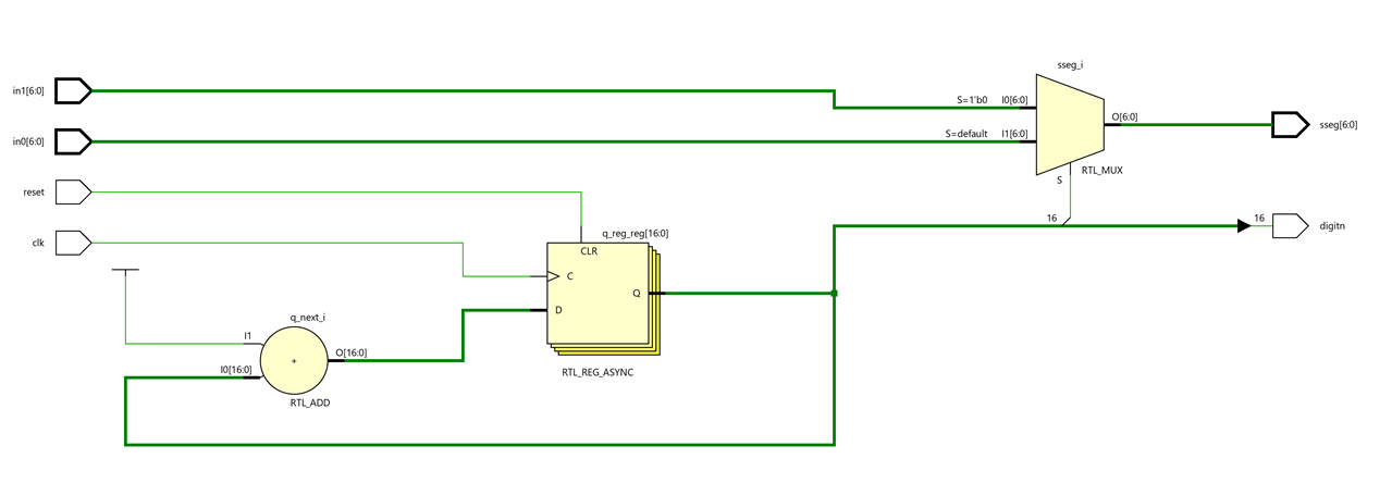
We will design a time-multiplexing circuit with a 1-to-2 decoder. It takes two seven patterns, in1, in0 and passes them to the output, sseg, in accordance with the digit enable signal digitn.
The refresh rate of the enable signal has to be fast enough to fool the human eyes but slow enough so that the LEDs can be turned on and off completely. 1000Hz should work properly.
We will use a 17-bit binary counter for this purpose. The MSB is decoded to generate the digit enable signal and is used as the selection signal for multiplexing.
We will connect the circuit with the Digilent Arty S7 50 100 MHz clock. Then the refreshing rate of an individual bit, such as in(0), becomes (100 000 000 / 2^16) Hz, 1526 Hz approx..
Block diagram of our time-multiplexing circuit with a 1-to-2 decoder.
2-to1 Time Multiplexing Circuit SystemVerilog Implementation.
A possible implementation for our 2-to1 Time Multiplexing circuit.
`timescale 1ns / 10ps

// time multiplexing with LED patterns.
// It takes two seven-segment LED patterns, in1, in0 and
// passes them to the output, sseg in accordance of the enable signal
// the refresh rate of the enable signal has to be fast enough to fool oureyes
// but slow enough so that the LEDs can be turned on and off completely
// Uses an 17-bit binary counter: The MSB is  decoded to generate the enable signal
// and are used as the selection signal for multiplexing.
// The refreshing rate of a bit as an(0) becomes 100 MHz / 2^16, 1600 Hz aprox
module disp_mux_2_1(
    input logic clk,
    input logic reset,
    input logic [6:0] in1,
    input logic [6:0] in0,
    output logic digitn, // digit selection
    output logic [6:0] sseg // led segments
);

    // refreshing rate around 1600 Hz (100 MHz/2^16)
    localparam N = 17;

    logic [N-1:0] q_reg;
    logic [N-1:0] q_next;

    // N-bit counter register
    always_ff @(posedge clk, posedge reset)
    begin
        if (reset)
            begin
                q_reg <=0;
            end
        else
            begin
                q_reg <= q_next;
            end
    end

    // next-state logic
    assign q_next = q_reg + 1;

    // 1 MSBs of counter to control 2 to 1 multiplexing
    // and to generate active enable signal
    always_comb
    begin
        case( q_reg[N-1])
            1'b0: begin
                sseg = in1;
                digitn = 1'b0;
            end
            default:  begin
                sseg = in0;
                digitn = 1'b1;
            end
        endcase
    end

endmodule
Multi-Digit Seven-Segment LED Display Time-Multiplexing Testing Circuit
We will use the following circuit to verify the operation of the LED display time-multiplexing circuit.
It is a simple 4-bit increment circuit to verify the operation of the decoder.
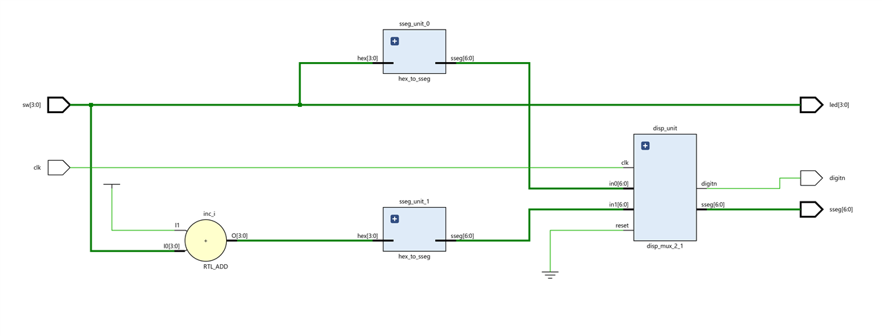
The sw input is connected to 4 slide switches of the prototyping board. It is fed to an incrementor to obtain sw+1.
The red leds on the board are also connected to the sw input so we can also "debug" the binary input.
The original sw and the incremented one sw+1 are passed to two hex-digit to seven-segment decoders to display the two hexadecimal digits on the Pmod SSD 2-digits seven-segment LED display.
LED display time-multiplexing circuit SystemVerilog Implementation
This is a possible implementation in SystemVerilog of the incrementor circuit with LED display time-multiplexing circuit :
`timescale 1ns / 10ps

module hex_to_sseg_test(
    input logic clk,
    input [3:0] sw,
    output logic digitn,
    output logic [6:0] sseg, // 7 led segments
    output logic [3:0] led
);

    logic [6:0] led0;
    logic [6:0] led1;

    logic [3:0] inc;

    // increment input
    assign inc = sw + 1;
    assign led = sw;

    // instantiate 2 instances of hex decoders
    // instantiate for sw input
    hex_to_sseg sseg_unit_0(.hex(sw[3:0]), .sseg(led0));
    // instantiate for incremented value
    hex_to_sseg sseg_unit_1(.hex(inc[3:0]), .sseg(led1));

    // instantiate 7-seg LED display time multiplexing module
     disp_mux_2_1 disp_unit(.clk(clk), .reset(1'b0), .in0(led0), .in1(led1), .digitn(digitn), .sseg(sseg));


endmodule
Constraint file
We need to mapping the logical port names of the test circuit to the physical signals on the Arty-S7 50 prototyping board.
## This file is a general .xdc for the Arty S7-50 Rev. E

## Clock Signals
set_property -dict { PACKAGE_PIN R2    IOSTANDARD SSTL135 } [get_ports { clk }]; #IO_L12P_T1_MRCC_34 Sch=ddr3_clk[200]
create_clock -add -name sys_clk_pin -period 10.000 -waveform {0 5.000}  [get_ports { clk }];

## Switches
set_property -dict { PACKAGE_PIN H14   IOSTANDARD LVCMOS33 } [get_ports { sw[0] }]; #IO_L20N_T3_A19_15 Sch=sw[0]
set_property -dict { PACKAGE_PIN H18   IOSTANDARD LVCMOS33 } [get_ports { sw[1] }]; #IO_L21P_T3_DQS_15 Sch=sw[1]
set_property -dict { PACKAGE_PIN G18   IOSTANDARD LVCMOS33 } [get_ports { sw[2] }]; #IO_L21N_T3_DQS_A18_15 Sch=sw[2]
set_property -dict { PACKAGE_PIN M5    IOSTANDARD SSTL135 } [get_ports { sw[3] }]; #IO_L6N_T0_VREF_34 Sch=sw[3]

## LEDs
set_property -dict { PACKAGE_PIN E18   IOSTANDARD LVCMOS33 } [get_ports { led[0] }]; #IO_L16N_T2_A27_15 Sch=led[2]
set_property -dict { PACKAGE_PIN F13   IOSTANDARD LVCMOS33 } [get_ports { led[1] }]; #IO_L17P_T2_A26_15 Sch=led[3]
set_property -dict { PACKAGE_PIN E13   IOSTANDARD LVCMOS33 } [get_ports { led[2] }]; #IO_L17N_T2_A25_15 Sch=led[4]
set_property -dict { PACKAGE_PIN H15   IOSTANDARD LVCMOS33 } [get_ports { led[3] }]; #IO_L18P_T2_A24_15 Sch=led[5]


## Pmod Header JA
set_property -dict { PACKAGE_PIN L17   IOSTANDARD LVCMOS33 } [get_ports { sseg[0] }]; #IO_L4P_T0_D04_14 Sch=ja_p[1]
set_property -dict { PACKAGE_PIN L18   IOSTANDARD LVCMOS33 } [get_ports { sseg[1] }]; #IO_L4N_T0_D05_14 Sch=ja_n[1]
set_property -dict { PACKAGE_PIN M14   IOSTANDARD LVCMOS33 } [get_ports { sseg[2] }]; #IO_L5P_T0_D06_14 Sch=ja_p[2]
set_property -dict { PACKAGE_PIN N14   IOSTANDARD LVCMOS33 } [get_ports { sseg[3] }]; #IO_L5N_T0_D07_14 Sch=ja_n[2]

## Pmod Header JB
set_property -dict { PACKAGE_PIN P17   IOSTANDARD LVCMOS33 } [get_ports { sseg[4] }]; #IO_L9P_T1_DQS_14 Sch=jb_p[1]
set_property -dict { PACKAGE_PIN P18   IOSTANDARD LVCMOS33 } [get_ports { sseg[5] }]; #IO_L9N_T1_DQS_D13_14 Sch=jb_n[1]
set_property -dict { PACKAGE_PIN R18   IOSTANDARD LVCMOS33 } [get_ports { sseg[6] }]; #IO_L10P_T1_D14_14 Sch=jb_p[2]
set_property -dict { PACKAGE_PIN T18   IOSTANDARD LVCMOS33 } [get_ports { digitn }]; #IO_L10N_T1_D15_14 Sch=jb_n[2]


## Configuration options, can be used for all designs
set_property BITSTREAM.CONFIG.CONFIGRATE 50 [current_design]
set_property CONFIG_VOLTAGE 3.3 [current_design]
set_property CFGBVS VCCO [current_design]
set_property BITSTREAM.CONFIG.SPI_BUSWIDTH 4 [current_design]
set_property CONFIG_MODE SPIx4 [current_design]

## SW3 is assigned to a pin M5 in the 1.35v bank. This pin can also be used as
## the VREF for BANK 34. To ensure that SW3 does not define the reference voltage
## and to be able to use this pin as an ordinary I/O the following property must
## be set to enable an internal VREF for BANK 34. Since a 1.35v supply is being
## used the internal reference is set to half that value (i.e. 0.675v). Note that
## this property must be set even if SW3 is not used in the design.
set_property INTERNAL_VREF 0.675 [get_iobanks 34]
The LED display time-multiplexing test circuit in action
The seven-segment LED digit on the left shows a hexadecimal representation of the 4-bit unsigned binary number represented by the positions of the 4 sliders.
The seven-segment LED digit to the right shows the value incremented by 1.
The red LEDs on the board change according to the change in the slide switches on the board.

SystemVerilog Study Notes Chapters
- Gate-Level Combinational Circuit
- RTL Combinational Circuit Operators
- RTL Combinational Circuit - Concurrent and Control Constructs
- Hex-Digit to Seven-Segment LED Decoder RTL Combinational Circuit
- Barrel Shifter RTL Combinational Circuit
- Simplified Floating Point Arithmetic. RTL Combinational Circuit
- BCD Number Format. RTL Combinational Circuit
- DDFS. Direct Digital Frequency Synthesis for Sound
- FPGA ADSR envelope generator for sound synthesis
- AMD Xilinx 7 series FPGAs XADC
- Building FPGA-Based Music Instrument Synthesis: A Simple Test Bench Solution