


I continue my series of notes on SystemVerilog as I learn. In this case I dedicate the study notes to Verilog operators as an introduction to combinational circuits. I'll cover always blocks and other routing constructs in a later blog.
Table of Contents
Chapters:
- Gate-Level Combinational Circuit
- RTL Combinational Circuit Operators
- RTL Combinational Circuit - Concurrent and Control Constructs
- Hex-Digit to Seven-Segment LED Decoder RTL Combinational Circuit
- Barrel Shifter RTL Combinational Circuit
- Simplified Floating Point Arithmetic. RTL Combinational Circuit
- BCD Number Format. RTL Combinational Circuit
- DDFS. Direct Digital Frequency Synthesis for Sound
- FPGA ADSR envelope generator for sound synthesis
- AMD Xilinx 7 series FPGAs XADC
- Building FPGA-Based Music Instrument Synthesis: A Simple Test Bench Solution
RT Level Combinational Circuit
Gate-level circuits utilize simple logical operators to describe gate-level design, which is composed of simple logic cells, like the circuits we designed in the previous blog. In this blog we will examine the HDL description of module-level circuits, which are composed of intermediate-sized components, such as adders, comparators, and multiplexers. These components are the basic building blocks in register-transfer methodology. The register transfer methodology (RT methodology) is a design methodology that describes system operation by a sequence of data transfers and manipulations among the registers. This methodology can support the variables and sequential execution of an algorithm and provide a systematic way to convert an algorithm into hardware. In a combinational circuit the output is a function of the input only.
First we need to learn more about SystemVerilog Operators in addition to the bitwise operators we used in the previous blog. In this blog we will present special attention to the operator syntax and its synthesis. Synthesis is the process of transforming an RTL-specified design into a gate-level representation. Vivado synthesis supports a synthesizable subset of SystemVerilog: IEEE Standard for SystemVerilog-Unified Hardware Design, Specification, and Verification Language (IEEE Std 1800-2012)
Reference: Vivado Design Suite User Guide: Synthesis
SystemVerilog Operators
Operators are single-, double-, or triple-character sequences and are used in expressions. Unary operators shall appear to the left of their operand. Binary operators shall appear between their operands. A conditional operator shall have two operator characters that separate three operands.
The symbols for the SystemVerilog operators are similar to those in the C programming language.
In addition to the bitwise operators, the arithmetic, shift, and relational operators can be synthesized. They correspond to intermediate-sized components, such as adders and comparators.
Operators syntax:
assignment_operator ::= = | += | -= | *= | /= | %= | &= | |= | ^= | <<= | >>= | <<<= | >>>=conditional_expression ::= cond_predicate ? { attribute_instance } expression : expressionunary_operator ::= + | - | ! | ~ | & | ~& | | | ~| | ^ | ~^ | ^~binary_operator ::= + | - | * | / | % | == | != | === | !== | ==? | !=? | && | || | ** | < | <= | > | >= | & | | | ^ | ^~ | ~^ | >> | << | >>> | <<< | -> | <->inc_or_dec_operator ::= ++ | --stream_operator ::= >> | <<
Operators and data types
| Operator token | Name | Operand data types |
= |
Binary assignment operator | Any |
+= -= /= *= |
Binary arithmetic assignment operators | Integral, real, shortreal |
%= |
Binary arithmetic modulus assignment operator | Integral |
&= |= ^= |
Binary bitwise assignment operators | Integral |
>>= <<= |
Binary logical shift assignment operators | Integral |
>>>= <<<= |
Binary arithmetic shift assignment operators | Integral |
?: |
Conditional operator | Any |
+ - |
Unary arithmetic operators | Integral, real, shortreal |
! |
Unary logical negation operator | Integral, real, shortreal |
~ & ~& | ~| ^ ~^ ^~ |
Unary logical reduction operators | Integral |
+ - * / ** |
Binary arithmetic operators | Integral, real, shortreal |
% |
Binary arithmetic modulus operator | Integral |
& | ^ ^~ ~^ |
Binary bitwise operators | Integral |
>> << |
Binary logical shift operators | Integral |
>>> <<< |
Binary arithmetic shift operators | Integral |
&& || –> <–> |
Binary logical operators | Integral, real, shortreal |
< <= > >= |
Binary relational operators | Integral, real, shortreal |
=== !== |
Binary case equality operators | Any except real and shortreal |
== != |
Binary logical equality operators | Any |
==? !=? |
Binary wildcard equality operators | Integral |
++ -- |
Unary increment, decrement operators | Integral, real, shortreal |
inside |
Binary set membership operator | Singular for the left operand |
dist |
Binary distribution operator | Integral |
{} {{}} |
Concatenation, replication operators | Integral |
{<<{}} {>>{}} |
Stream operators | Integral |
Integral types refer to the data types that can represent a single basic integer data type, packed array, packed structure, packed union, enum variable, or time variable.
The real data type is the same as a C double. The shortreal data type is the same as a C float.
Vivado synthesis supports the following SystemVerilog operators:
- Assignment operators (=,+=, -=, *=, /=, %=, &=, |=, ^=, <<=, >>=, <<<=, >>>=)
- Unary operators (+, -, !, ~, &, ~&, |, ~|, ^, ~^, ^~)
- Increment/decrement operators (++, --)
- Binary operators (+, -, *, /, %, ==, ~=, ===, ~==, &&, ||, **, <, <=, >, >=, &, |, ^, ^~, ~^, >>, <<, >>>, <<<) Note: A**B is supported if A is a power of 2 or B is a constant.
- Conditional operator (? :)
- Concatenation operator ({...})
Arithmetic Operators
There are six arithmetic operators:
- + : addition
- - : subtraction
- * : multiplication
- / : division
- % : modulus
- ** : exponentiation
Arithmetic Operators Synthesis
- + and - infer the adder and subtractor. They are synthesized by FPGA's logic cells
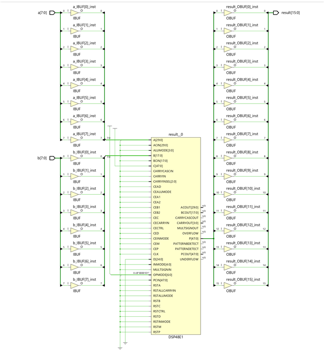
- * : Synthesizing multiplication from normal logic cells consumes a lot of resources. Xilinx Spartan-7 FPGA family embeds 160 DSP slices. Each DSP slice contains a pre-adder, a 25 x 18 multiplier, an adder, and an accumulator. Vivado software can infer these for the * operator. While the multiplication operator is supported, we need to be aware of the limitation on the number and input width of the multiplier macro cells and use them with care.
- /, %, ** : usually cannot be synthesized automatically but can be used in static expressions,
Vivado synthesized automatically +, -, *, / and % but ** only in special conditions.
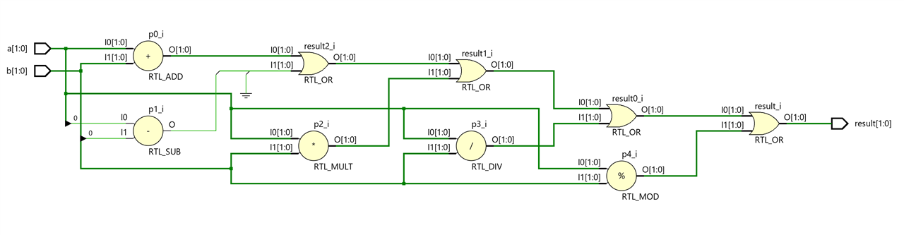
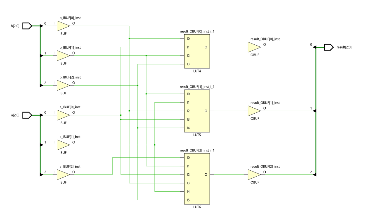
module arithmetic_2_bits(
    input logic [1:0] a,
    input logic [1:0] b,
    output logic [1:0] result
    );

    logic [1:0] p0;
    logic [1:0] p2;
    logic [1:0] p3;
    logic [1:0] p4;


    assign result = p0 | p1 | p2 | p3 | p4 ;

    assign p0 = a + b;
    assign p1 = a - b;
    assign p2 = a * b;
    assign p3 = a / b;
    assign p4 = a % b;
    // assign p5 = a ** b;

endmodule
RTL Analysis Elaborated Design Schematic
Just out of curiosity let's see how Vivado synthesizes a multiplier from 8 bits to 16 bits. 8 bit x 8 bit multiplication. SystemVerilog code:
`timescale 1ns / 10ps

module multiplier_8_bits(
    input [7:0] a,
    input [7:0] b,
    output [15:0] result
    );

    assign result = a * b;

endmodule
Testbech
`timescale 1ns / 10ps

module multiplier_8_bits_testbench(

    );
    logic [7:0] a;
    logic [7:0] b;
    logic [15:0] result;

    multiplier_8_bits uut(.*);

    initial
    begin
        a = 8'd0;
        b = 8'd0;
        #200;
        a = 8'd255;
        b = 8'd0;
        #200;
        a = 8'd255;
        b = 8'd1;
        #200;
        a = 8'd0;
        b = 8'd255;
        #200;
        a = 8'd1;
        b = 8'd255;
        #200;
        a = 8'd255;
        b = 8'd255;
        #200;
        $stop;
    end
endmodule
Simulation
This is the Synthesized Design. By default it is not using DSP Blocks.
Vivado synthesis infers Multiplier macros from multiplication operators in the source code. The resulting signal width equals the sum of the two operand sizes. For example, multiplying a 16-bit signal by an 8-bit signal produces a result of 24 bits.
Vivado Design Suite User Guide: Synthesis (UG901)
Multiplier macros can be implemented on Slice logic or on DSP blocks. The implementation choice is driven by the size of operands, aimed at maximizing performance.
To force implementation of a Multiplier to slice logic or DSP block, set the USE_DSP attribute on the appropriate signal, entity, or module to either: no (slice logic) or yes (DSP block)
`timescale 1ns / 10ps

(* use_dsp48 = "yes" *) module multiplier_8_bits(
    input logic [7:0] a,
    input logic [7:0] b,
    output logic [15:0] result
    );

    assign result = a * b;
endmodule
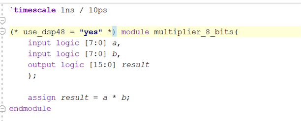
And now it is using DSP Bloks
Vivado Synthesized Design Schematics
Shift Operators
There are four shift operators operators:
- >> : logical shift right. 0's are shifted in
- << : logical shift left. 0's are shifted in
- >>> : arithmetic shift right. Sign bits (i.e., MSB) are shifted
- <<< : arithmetic shift left. 0's are shifted in. << and <<< are equal
`timescale 1ns / 1ps

module shift_operators(
    input logic [7:0] a,
    output logic [7:0] logic_right,
    output logic [7:0] logic_left,
    output logic [7:0] arithmetic_right,
    output logic [7:0] arithmetic_left
);

    assign logic_right = a >> 2;
    assign logic_left = a << 2;
    assign arithmetic_right = a >>> 2;
    assign arithmetic_left = a <<< 2;

endmodule
Testbench:
`timescale 1ns / 10ps

module shift_operators_testbench();
    logic [7:0] a;
    logic [7:0] logic_right;
    logic [7:0] logic_left;
    logic [7:0] arithmetic_right;
    logic [7:0] arithmetic_left;

    shift_operators uut(.*);

    initial
    begin
        a = 8'b0100_1111;
        #200;
        a = 8'b1100_1111;
        #200;
        $stop;
    end
endmodule
Sumulation
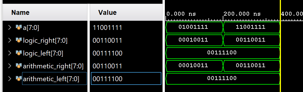
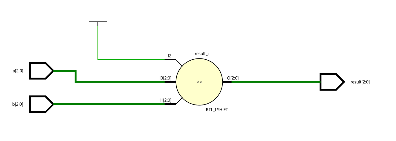
Some textbooks indicate that if both operators are signals of a shift operator are signals, as in a << b, a barrel shifter is inferred, but it seems that this is not the case. I haven't seen any indication of this behavior in the SystemVerilog standard either.
module shift_infer_barrel_shifter(
    input logic [2:0] a,
    input logic [2:0] b,
    output [2:0] result
    );

    assign result = a << b;
endmodule
Vivado RTL Analysis Elaborated Design Schematic
`timescale 1ns / 10ps


module barrel_shifter_built_in(
    input logic [7:0] data,
    input logic [2:0] amt,
    output logic [7:0] out
    );

    assign out = data >> amt;

endmodule


module barrel_shifter_built_in_testbench;
    logic [7:0] data;
    logic [2:0] amt;
    logic [7:0] out;

    barrel_shifter_built_in uut(.*);

    initial begin
      for (byte i = 1; i < 8; ++i)
      begin
         data = 8'b1111_0000; amt = 3'(i); #10;
      end
      $stop;
    end

endmodule
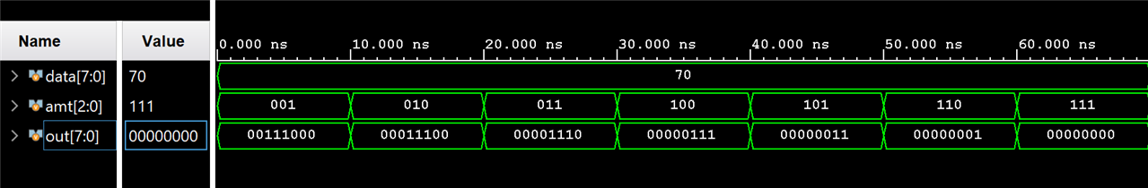
Vivado Synthesized Design Schematics
Relational and Equality Operators
- Relational operators: >, < , <= , >= . These operators compare two operands and return a Boolean value, false (1-bit scalar value 0) or true (1-bit scalar value 1)
- Equality operators: ==, !=, ===, and !==. These operators returns false or true
The === and !== are case equality and case inequality, take in consideration of the matches of the x and z bits in the operands and cannot be synthesized.
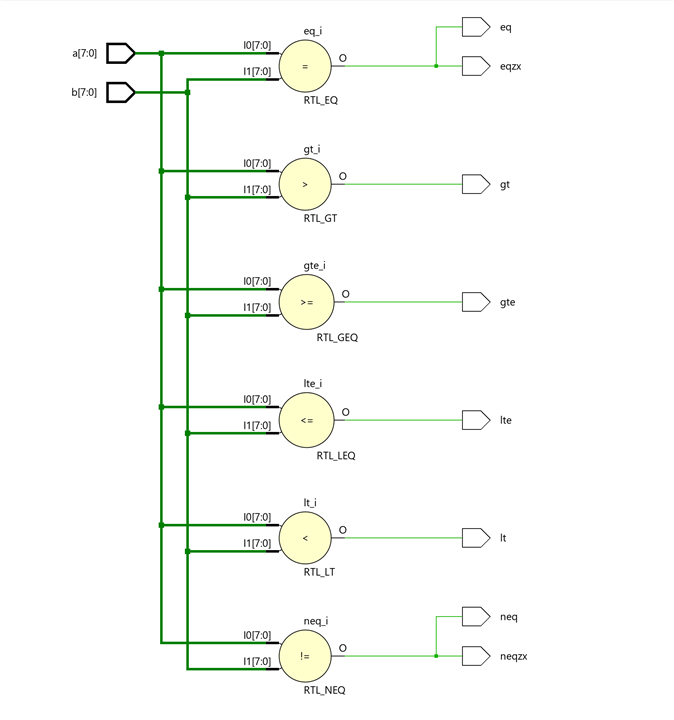
`timescale 1ns / 1ps

module relational_operators(
    input logic [7:0] a,
    input logic [7:0] b,
    output logic gt,
    output logic lt,
    output logic lte,
    output logic gte,
    output logic eq,
    output logic neq,
    output logic eqzx,
    output logic neqzx
    );

    assign gt = a > b;
    assign lt = a < b;
    assign lte = a <= b;
    assign gte =a >= b;
    assign eq =a == b;
    assign neq =a != b;
    assign eqzx = a === b;
    assign neqzx = a !== b;

endmodule
Testbench
`timescale 1ns / 10ps


module relational_operators_testbench(

);

    logic [7:0] a;
    logic [7:0] b;
    logic gt;
    logic lt;
    logic lte;
    logic gte;
    logic eq;
    logic neq;
    logic eqzx;
    logic neqzx;

    relational_operators uut(.*);

    initial
    begin
        a = 8'd200;
        b = 8'd10;
        #200
        a = 8'd10;
        b = 8'd10;
        #200
        a = 8'd99;
        b = 8'd100;
        #200
        a = 8'b0011_0z000;
        b = 8'b0011_01000;
        #200
        a = 8'b0011_0x000;
        b = 8'b0011_01000;
        #200
        a = 8'b0011_0xzxz;
        b = 8'b0011_01000;
        #200
        $stop;
    end
endmodule
Simulation
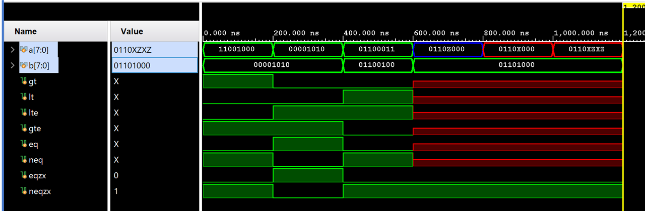
RTL Analysis Elaborated Design Schematic
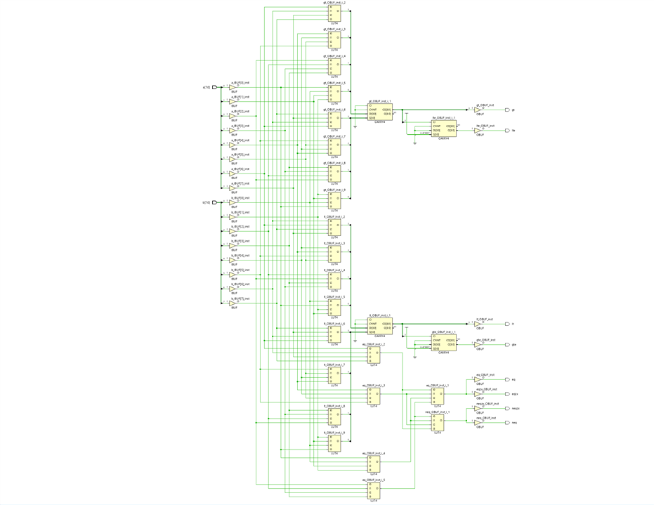
The (===) and (!==) operators are special comparison operators, used in simulation to see if a variable is assigned a value of (x) or (z) but treated as (==) or (!=) by synthesis.
Vivado Synthesized Design Schematics
Evaluated Expressions Based On Most Frequently Used Operator
|
a b |
a==b |
a===b |
a!=b |
a!==b |
a&b |
a&&b |
a|b |
a||b |
a^b |
|---|---|---|---|---|---|---|---|---|---|
|
0 0 |
1 |
1 |
0 |
0 |
0 |
0 |
0 |
0 |
0 |
|
0 1 |
0 |
0 |
1 |
1 |
0 |
0 |
1 |
1 |
1 |
|
0 x |
x |
0 |
x |
1 |
0 |
0 |
x |
x |
x |
|
0 z |
x |
0 |
x |
1 |
0 |
0 |
x |
x |
x |
|
1 0 |
0 |
0 |
1 |
1 |
0 |
0 |
1 |
1 |
1 |
|
1 1 |
1 |
1 |
0 |
0 |
1 |
1 |
1 |
1 |
0 |
|
1 x |
x |
0 |
x |
1 |
x |
x |
1 |
1 |
x |
|
1 z |
x |
0 |
x |
1 |
x |
x |
1 |
1 |
x |
|
x 0 |
x |
0 |
x |
1 |
0 |
0 |
x |
x |
x |
|
x 1 |
x |
0 |
x |
1 |
x |
x |
1 |
1 |
x |
|
x x |
x |
1 |
x |
0 |
x |
x |
x |
x |
x |
|
x z |
x |
0 |
x |
1 |
x |
x |
x |
x |
x |
|
z 0 |
x |
0 |
x |
1 |
0 |
0 |
x |
x |
x |
|
z 1 |
x |
0 |
x |
1 |
x |
x |
1 |
1 |
x |
|
z x |
x |
0 |
x |
1 |
x |
x |
x |
x |
x |
|
z z |
x |
1 |
x |
0 |
x |
x |
x |
x |
x |
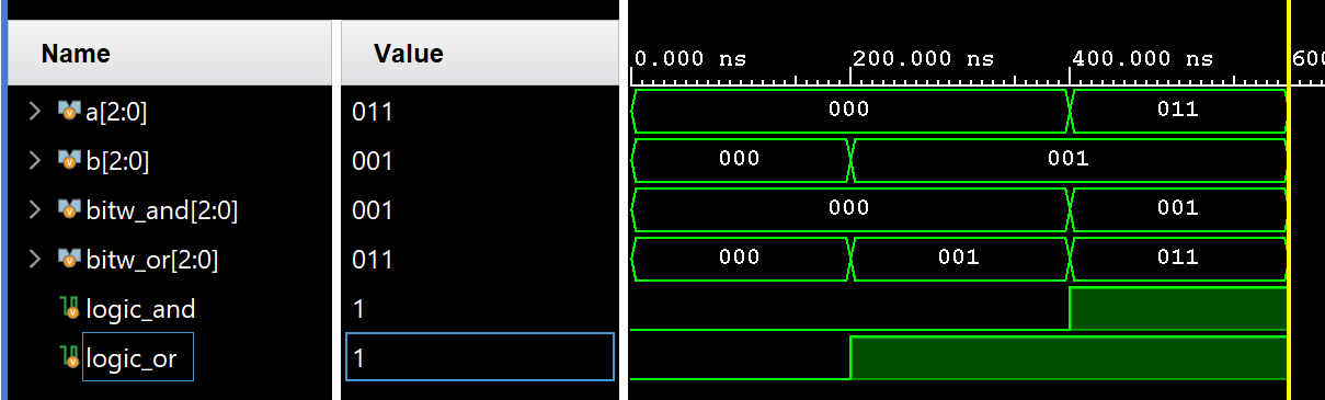
Bitwise, reduction and logical operators
Bitwise operators: & (and), | (or), ^ (xor) and ~ (not). Negation and xor can be combined as ~^ or ^~, to form xnor operator. Operations are performed on a bit-by-bit basis
Reduction operators: &, | and ^ may have only one operand. If the operand is an array data type the operation is performed on all elements of the array and returns 1-bit result.
Logical operators: && (logical and), || (logical or), ! (logical negate). If x or z are not used the operands of a logical operator are interpreted as false (all bits are 0's) or true (at least one bit is 1). Always return 1-bit result.
`timescale 1ns / 1ps

module logical_bitwise_operators(
    input logic [2:0] a,
    input logic [2:0] b,
    output logic [2:0] bitw_and,
    output logic [2:0] bitw_or,
    output logic logic_and,
    output logic logic_or
    );

    assign bitw_and = a & b;
    assign bitw_or = a | b;
    assign logic_and = a && b;
    assign logic_or = a || b;

endmodule
Testbench
`timescale 1ns / 10ps

module logical_bitwise_testbench();

    logic [2:0] a;
    logic [2:0] b;
    logic [2:0] bitw_and;
    logic [2:0] bitw_or;
    logic logic_and;
    logic logic_or;

    logical_bitwise_operators uut(.*);

    initial
    begin

        a=3'b000;
        b=3'b000;
        #200

        a=3'b000;
        b=3'b001;
        #200

        a=3'b011;
        b=3'b001;
        #200

        $stop;
    end

endmodule
Simulation
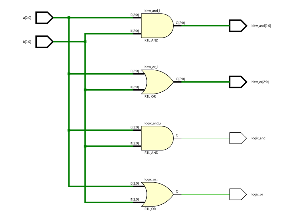
RTL Analysis Elaborated Design Schematic
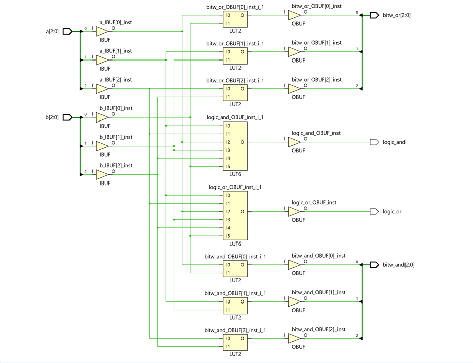
Vivado Synthesized Design Schematics
Concatenation and replication operators
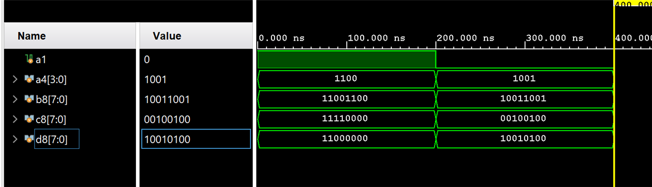
The concatenation operator, { }, combines segments of elements and small arrays to form a larger array.
The concatenator operator, N{ }, replicates the enclosed string. Vivado doesn't support the N{ } operator
`timescale 1ns / 1ps

module concatenation(
    input logic a1,
    input logic [3:0] a4,
    output logic [7:0] b8,
    output logic [7:0] c8,
    output logic [7:0] d8
    );

    assign b8 = {a4, a4};
    assign c8 = {a1, a1, a4, 2'b00};
    assign d8 = {b8[3:0], c8[3:0]};
endmodule
Testbench
`timescale 1ns / 10ps

module concatenation_testbench;
    logic a1;
    logic [3:0] a4;
    logic [7:0] b8;
    logic [7:0] c8;
    logic [7:0] d8;

    concatenation uut(.*);

    initial
    begin

        a1 = 1'b1;
        a4 = 4'b1100;
        #200

        a1 = 1'b0;
        a4 = 4'b1001;
        #200
        $stop;
    end
endmodule
assign b8 = {a4, a4}; assign c8 = {a1, a1, a4, 2'b00}; assign d8 = {b8[3:0], c8[3:0]};
Simulation
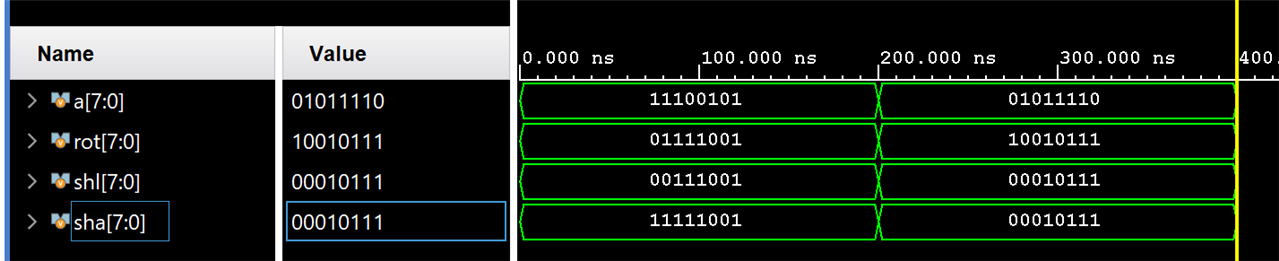
Rotate a signal by a fixed amount.
`timescale 1ns / 1ps

module rotate_signal_n(
    input logic [7:0] a,
    output logic [7:0] rot,
    output logic [7:0] shl,
    output logic [7:0] sha
    );

    // rotate a to right 3 bits
    assign rot = {a[2:0], a[7:2]};

    // shift to right 3 bits and insert 0 (logic shift)
    assign shl = {3'b000, a[7:2]};

    // shift to right 3 bits and insert MSB
    // (arithmetic shift)
    assign sha = {a[7], a[7], a[7], a[7:2]};
endmodule
Testbench
`timescale 1ns / 1ps
module rotate_signal_testbench;

    logic [7:0] a;
    logic [7:0] rot;
    logic [7:0] shl;
    logic [7:0] sha;

    rotate_signal_n uut(.*);

    initial
    begin
      a = 8'b1110_0101;
      #200
      a = 8'b0101_1110;
      #200
      $stop;
    end

endmodule
Simulation
Vivado elaborated design schematic
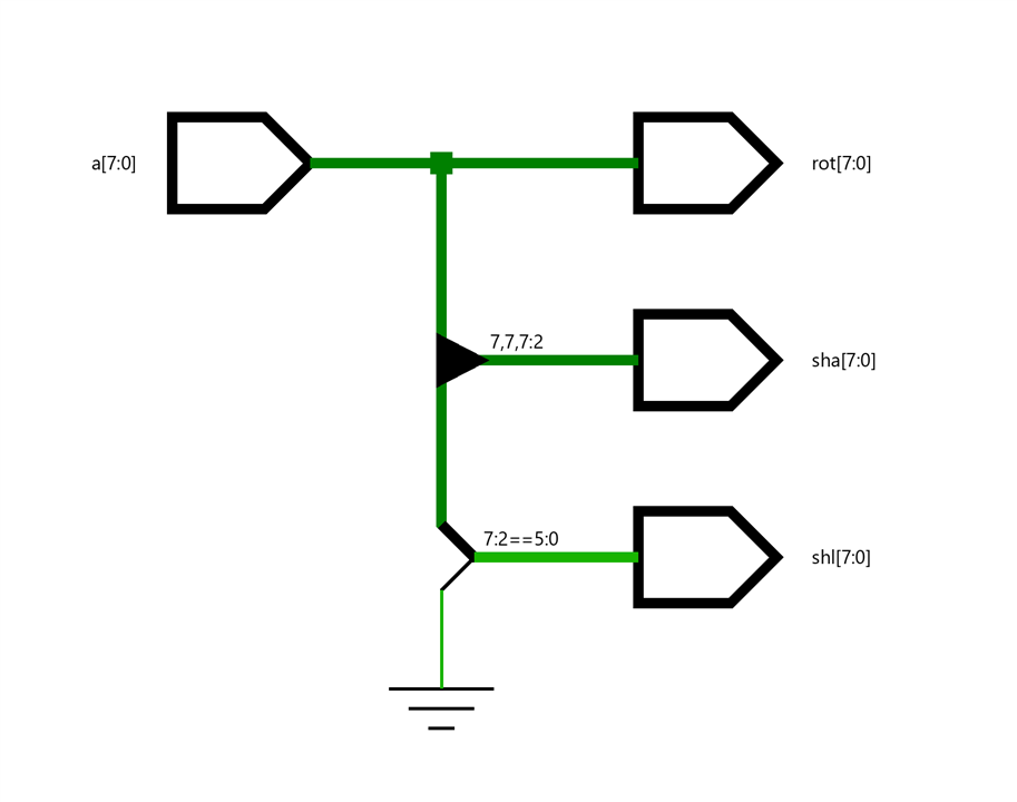
Implementation of the concatenation operator involves reconnection of the input and output signals and only requires "wiring"
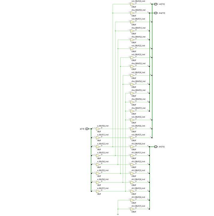
Vivado synthesized design schematic:
Conditional Operators
The conditional operator ?:, takes three operands and its general format is:
[signal] = [boolean_exp] ? [true_exp] : [false_exp];
The [boolean_exp] is a Boolean expresion that return true (1'b1) or false (1'b0).
The [signal] gets [true_exp] if it is true and [false_exp] if it is false.
Conditional operators can be cascaded or nested.
Lets describe the eq1 circuit describe in the previous post:
assign eq = (~b & ~a) ? 1'b1 :
(~b & a) ? 1'b0 :
(b & ~a) ? 1'b0 :
1'b1;
Comparing the three versions of eq1. The three elaborated versions give the same results.
Operator precedence
The operator precedence specifies the order of evaluation. We can use parenthesis to alter the precedence or to make an expression clearer.
| Operator | Associativity | Precedence |
() [] :: . |
Left | Highest |
+ - ! ~ & ~& | ~| ^ ~^ ^~ ++ -- (unary) |
||
** |
Left | |
* / % |
Left | |
+ - (binary) |
Left | |
<< >> <<< >>> |
Left | |
< <= > >= inside dist |
Left | |
== != === !== ==? !=? |
Left | |
& (binary) |
Left | |
^ ~^ ^~ (binary) |
Left | |
| (binary) |
Left | |
&& |
Left | |
|| |
Left | |
?: (conditional operator) |
Right | |
–> <–> |
Right | |
= += -= *= /= %= &= ^= |= <<= >>= <<<= >>>= := :/ <= |
None | |
{} {{}} |
Concatenation | Lowest |
Expression bit-length adjustment
In SystemVerilog the bit length of operands can be different.
The number of bits of an expression (known as the size of the expression) shall be determined by the operands involved in the expression and the context in which the expression is given.
A self-determined expression is one where the bit length of the expression is solely determined by the expression itself—for example, an expression representing a delay value.
A context-determined expression is one where the bit length of the expression is determined by the bit length of the expression and by the fact that it is part of another expression. For example, the bit size of the right-hand expression of an assignment depends on itself and the size of the left-hand side.
The adjustment is determined by a set of implicit rules:
- Determine the maximal bit length of the operands in the context, which includes the right-hand side expression and the left-hand side signal.
- Extends the bit lengths of operands on the right-hand expression to the maximum and evaluate the expression.
- Assign the result to the left-hand-side signal, Truncate the MSBs if the signal's it length is smaller.
The following table shows how the form of an expression shall determine the bit lengths of the results of the expression.
i, j, and k represent expressions of an operand, and L(i) represents the bit length of the operand represented by i.
| Expression | Bit length | Comments |
| Unsized constant number | Same as integer | |
| Sized constant number | As given | |
|
i op j, where op is: |
max(L(i),L(j)) | |
|
op i, where op is:
|
L(i) | |
|
i op j, where op is:
|
1 bit | Operands are sized to max(L(i),L(j)) |
|
i op j, where op is:
|
1 bit | All operands are self-determined |
|
op i, where op is:
|
1 bit | All operands are self-determined |
|
op j, where op is:
|
L(i) | j is self-determined |
i ? j : k |
max(L(j),L(k)) | i is self-determined |
{i,...,j} |
L(i)+..+L(j) | All operands are self-determined |
{i{j,..,k}} |
i x (L(j)+..+L(k)) | All operands are self-determined |
Synthesis of z and x values
A variable can contain z and x values in addition to logic 0 and 1.
Synthesis of z
z value implies high impedance or an open circuit. It is not a normal logic value an can only be synthesized by a tristate buffer.
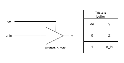
The operation of the buffer is controlled by an enable signal, oe (output enable)
The logic data type is intended for the normal design and does not support multiple drivers. To model the tristate behaviors, we must use the tri or wire data type
`timescale 1ns / 10ps
module tristate_buffer(
input logic a_in,
input logic oe,
output tri y
);
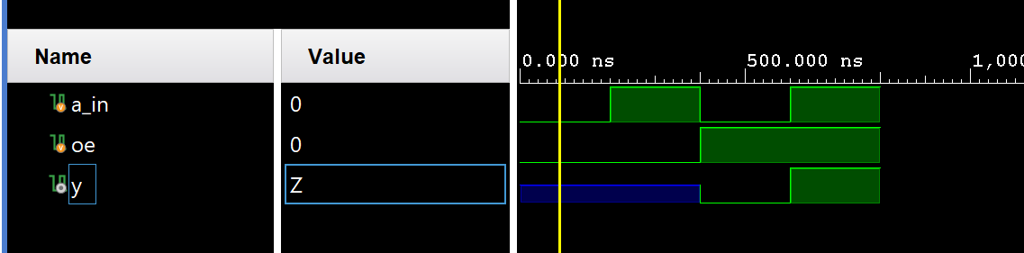
assign y = (oe) ? a_in : 1'bz;
endmodule
Testbench
`timescale 1ns / 10ps

module tristate_buffer_testbench;

    logic a_in;
    logic oe;
    tri y;

    tristate_buffer uut(.*);

    initial
        begin

        a_in = 1'b0;
        oe = 1'b0;
        #200

        a_in = 1'b1;
        oe = 1'b0;
        #200

        a_in = 1'b0;
        oe = 1'b1;
        #200

        a_in = 1'b1;
        oe = 1'b1;
        #200

        $stop;
        end
endmodule
Simulation
Vivado elaborated design schematic
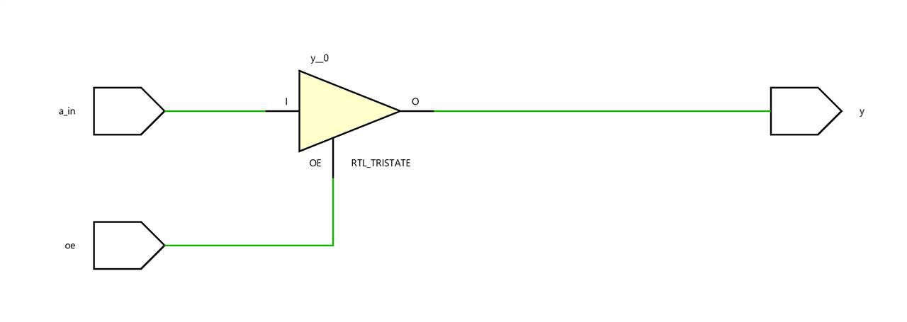
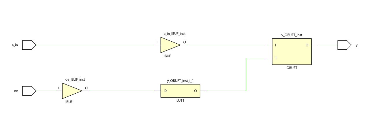
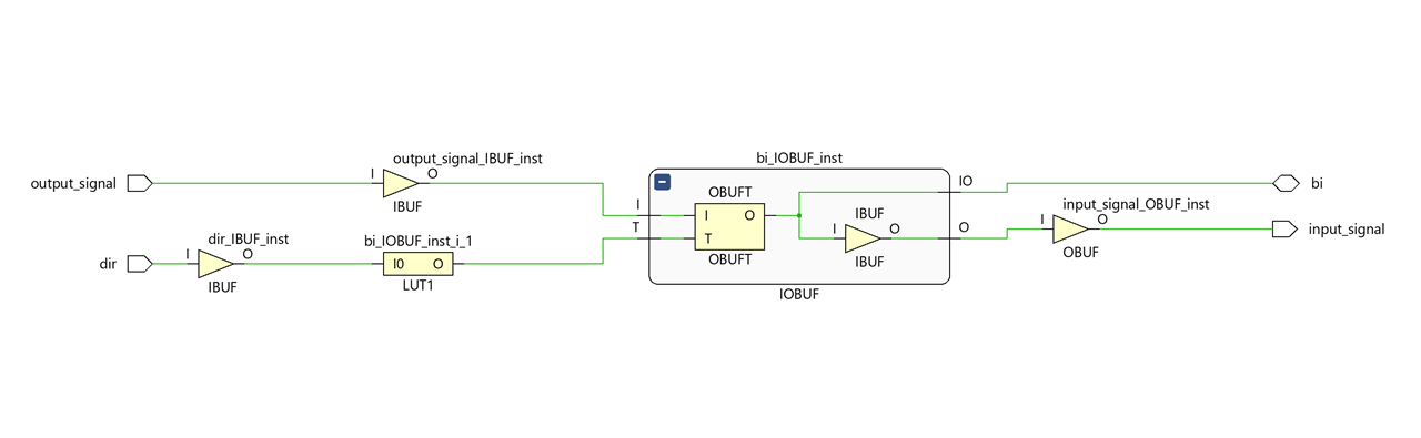
Tristate Implementation: Inferred Tristate buffers are implemented with different device primitives when driving the following:
- An external pin of the circuit (OBUFT)
- An Internal bus (BUFT):
- An inferred BUFT is converted automatically to logic realized in LUTs by Vivado synthesis.
- When an internal bus inferring a BUFT is driving an output of the top module, the Vivado synthesis infers an OBUF.
The tristate buffer exists only in the I/O macro cell.
Vivado Synthesized Design Schematics
It is used to implement a bidirectional port to better utilize a physical I/O pin.
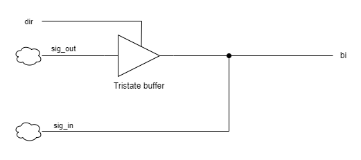
The dir signal controls the direction of the signal flow of the bi pin:
- When it is 0, the tristate buffer is in high-impedance state and the sig_out signal is blocked. The pin is used as an input port and the input signal is routed to the sig_in signal.
- When it is 1, the pin is used as an output port and the sig_out signal is routed to an external circuit.
`timescale 1ns / 1ps

module bi_demo(
    inout tri bi,
    input logic dir,
    input logic output_signal,
    output logic input_signal
    );

    assign bi = (dir) ? output_signal : 1'bz;
    assign input_signal = bi;

endmodule
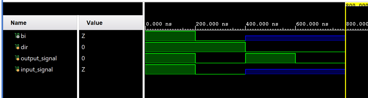
Testbench
`timescale 1ns / 10ps

module bi_demo_testbench;

    tri bi;
    logic dir;
    logic output_signal;
    logic input_signal;

    bi_demo uut(.*);

    initial
    begin
        dir = 1'b1;
        output_signal = 1;
        #200;
        dir = 1'b1;
        output_signal = 0;
        #200;
        dir = 1'b0;
        output_signal = 1;
        #200;
        dir = 1'b0;
        output_signal = 0;
        #200;

        $stop;
    end
endmodule
Vivado elaborated design schematic
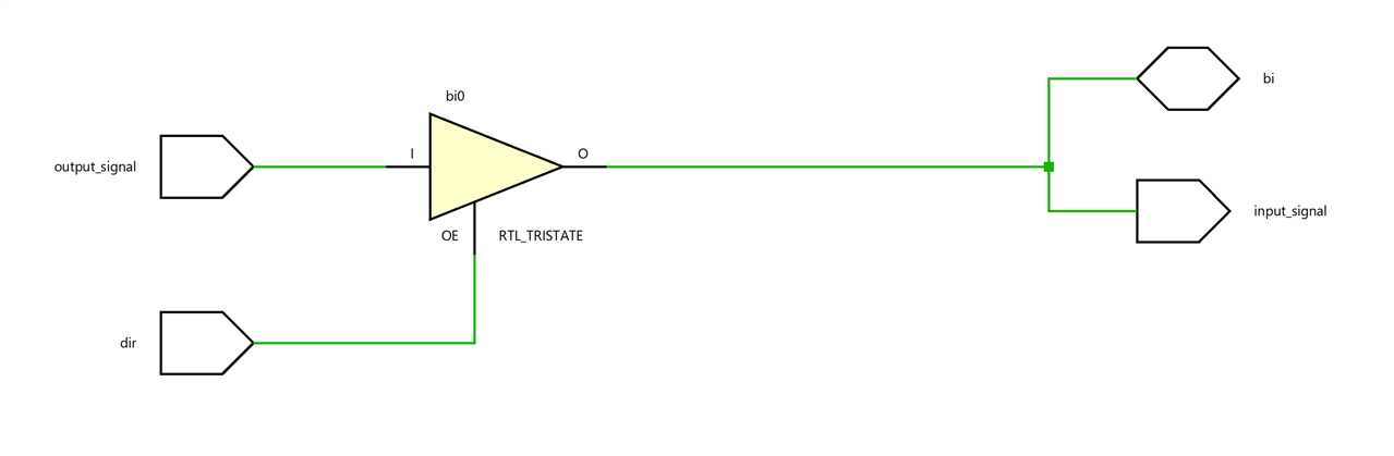
Vivado Synthesized Design Schematics
Synthesis of x
When in a combinational circuit certain input patterns may never occur we frequently assign a "don't-care" value to the output.
During the synthesis a value will be assigned to the don't care value, this can help the optimization process. This approach introduces a discrepancy between simulation and synthesis.
In simulation, x is a unique value rather than "0 or 1". In the synthetized result it will be either 0 or 1.
Source files
Conclusion
SystemVerilog consists of about sixty operators. These operators correspond to intermediate-sized components, such as adders and comparators. We have seen how Vivado synthesizes some of them for the case of the Spartan-7 FPGA on the Arty S7 50 board. We have also seen how to tell the Vivado synthesizer to use the multipliers of the DSP blocks included in the Spartan-7 FPGAs.
We leave the always block and routing constructors for a later blog.
SystemVerilog Study Notes Chapters
- Gate-Level Combinational Circuit
- RTL Combinational Circuit Operators
- RTL Combinational Circuit - Concurrent and Control Constructs
- Hex-Digit to Seven-Segment LED Decoder RTL Combinational Circuit
- Barrel Shifter RTL Combinational Circuit
- Simplified Floating Point Arithmetic. RTL Combinational Circuit
- BCD Number Format. RTL Combinational Circuit
- DDFS. Direct Digital Frequency Synthesis for Sound
- FPGA ADSR envelope generator for sound synthesis
- AMD Xilinx 7 series FPGAs XADC
- Building FPGA-Based Music Instrument Synthesis: A Simple Test Bench Solution