How Do You Build a Power MOSFET?
A power MOSFET is a metal-oxide-silicon field-effect transistor designed to manage high power levels with high switching speed and optimal efficiency. This technology is central to a broad range of applications including, consumer electronics, DC-to-DC converters, motor controllers, radio-frequency (RF) devices, and automotive electronics. Power MOSFETs are now the standard choice for main switching devices over a broad sweep of power conversion applications. Most of them are carrier devices and require low gate drive power due to the insulated gate. Power MOSFETs reduce power dissipation, which in turn reduces size and overall system cost.
The type and material of power MOSFET used directly impacts overall performance, whatever the application. It is thus essential to choose the right technology. Silicon Carbide (SiC), a wide-bandgap (WBG) semiconductor, has emerged as a viable option for replacing Silicon (Si). SiC-based power MOSFETs offer several performance advantages, as well as improved efficiency. SiC-based products range from ultra-low to high-voltage power devices, and have sweet spots in voltage classes at and above 650V.
|
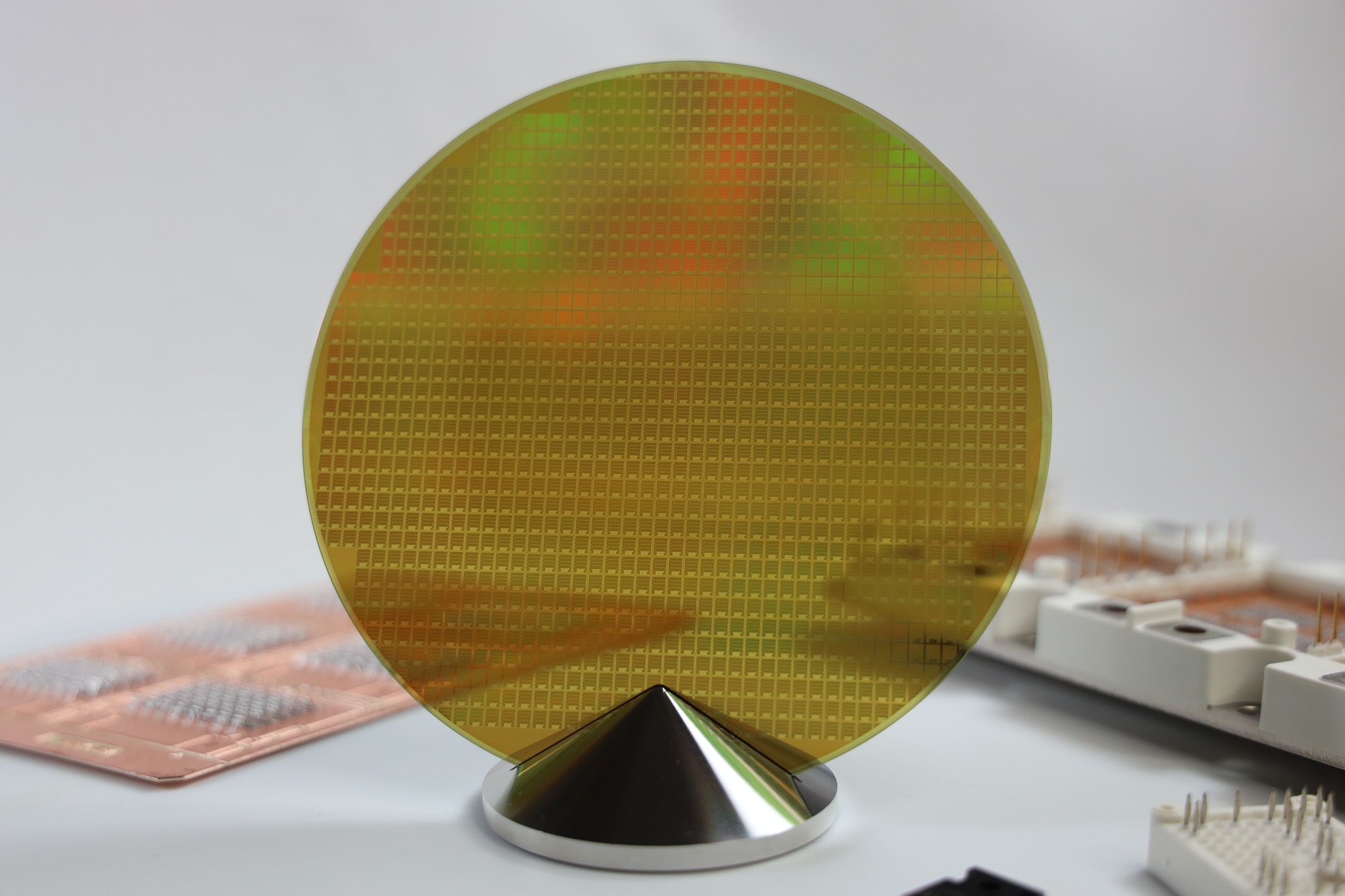
What is Silicon Carbide? SiC (aka Carborundum) is a stable compound semiconductor consisting of silicon (Si) and carbon (C). It exists in a variety of polymorphic crystalline structures called polytypes. The material is thermally, chemically, and mechanically stable, and satisfies all the parameters necessary for power devices. The most widely adopted structures for semiconductor use are 3C, 4C, and 6H polytype, all of which have different electrical properties and advantages when doped with various elements. Figure 1: Silicon Wafer
SiC’s main attractions stem from a single physical feature: SiC’s bandgap, the energy needed to excite electrons from the material’s valence band to the conduction band.. Table 1 summarizes the physical property differences between Si and SiC.
SiC can serve the bulk of applications on the power spectrum, from low-power devices to high-power systems, due to its unique combination of:
On the transistor level, this leads to a low on-state resistance (RDS(on)) that allows for lower conduction losses, which, in turn, allows all high-current applications. |
The Differences Between Silicon and Silicon Carbide
SiC has several advantages over Si when used in semiconductor technology. Using SiC in place of Si results in:
- Smaller sizes – SiC semiconductors can be up to 10 times smaller for the same performance
- Reduced heat loss (up to 50% less), due to lower resistance
- Faster operation, due to increased switching frequencies
- High-temperature operation - SiC semiconductors can maintain functionality and integrity at 200°C or more, due to WBG and thermal conductivity properties
- Higher Voltage operation – SiC can withstand voltages up to 10 times higherthan ordinary Si. SiC devices rated at 650V, 1,200V, and 1,700V and beyond are now commercially available.
- Lower energy losses - as a WBG material, SiC has a low gate charge, implying that SiC needs far less energy to make the device switch.
- Lower reverse recovery time due to lower energy losses - the energy lost by SiC during the reverse recovery phase is typically just one percent of the energy lost by Si.
- Lower system cost - SiC MOSFETs simplify switching frequency and thermal management, leading to reduced PC board form factors and fewer components.
- SiC delivers 10x the mean time to failure (MTTF) of Si. It is also 30x less sensitive to radiation and single event failure.
- Longer life span. The above-stated factors lead to a longer life span, along with a more reliable structure and system.
Figure 2 illustrates some of the advantages of using a 5kV semiconductor device. When working with Si, semiconductor designers are forced to use a relatively thick active zone because of the moderate internal breakdown field. In addition, only a few dopants can be incorporated in the active area, thus resulting in high series resistance. With SiC’s ten times higher breakdown field, the active zone can be made much thinner and many more free carriers can be incorporated, resulting in higher conductivity. The thinner and more highly doped drift layer leads to a much lower resistance. As a consequence, there is low forward voltage and low conduction loss, while maintaining high blocking voltage.
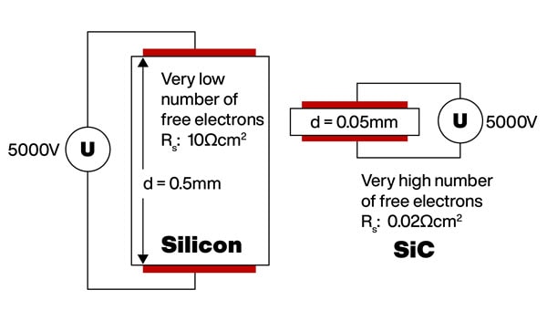
Figure 2: SiC allows for thinner semiconductor active zones
Source:https://www.infineon.com/dgdl/Infineon-CoolSiC_MOSFET_technology-Article-v01_00-EN.pdf?fileId=5546d4626d66c2b1016d6c4c5bdc407c
Silicon Carbide in MOSFETs
The Si MOSFET has proved to be a time-tested option for low-voltage applications; however, these devices exhibit large on-state resistance (RDS(on)) values at high voltage levels (> 600V), leading to higher conduction loss. In addition to requiring complex cooling systems, higher conduction losses result in reduced system efficiency and lower power density. An alternative using the same semiconductor material is an Si IGBT device, which satisfies the requirement for higher blocking voltage with low on-state resistance. Its bipolar nature, however, can impose limitations on maximum achievable switching frequency.
The material properties of SiC offer the opportunity to combine high blocking voltage capabilities and low specific on-state resistance in a unipolar device, allowing for incredibly fast switching speeds. In both Si and SiC devices, the absolute resistance is defined by the series connection of contact resistances at drain and source. These include the highly doped areas close to the contact, the channel resistance, the resistance of the JFET (Junction Field-Effect Transistor) area, and the drift zone resistance (Figure 3).
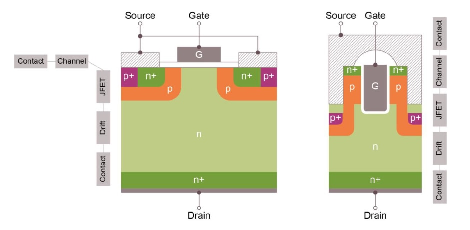
Figure 3: Sketch of a planar DMOS SiC MOSFET (left), and a vertical trench TMOS SiC MOSFET (right), and corresponding locations of resistance-relevant contributions
Source:https://www.infineon.com/dgdl/Infineon-High-performance_CoolSiC_MOSFET_technology_with_silicon-like_reliability-Whitepaper-v01_00-EN.pdf?fileId=5546d4626f229553016f8f5c95f02c54&da=t
Most SiC MOSFETs are presently based on either planar DMOS (Double Diffused MOS) or Trench MOS (TMOS)-like design structures. To mitigate the low conductivity of the planar channel of a DMOS SiC MOSFET, the electric field applied across the oxide in the on-state is increased. DMOS SiC MOSFETs use voltages in the range of 4-5 MV/cm, whereas typical Si MOSFETs use a maximum of 3 MV/cm. Thus, special care must be taken in the DMOS structure, particularly concerning the potential high field failure rate due to the quite high permanent on-state gate oxide stress fields.
The struggle between performance and robustness is mitigated with a structure known as a "trench". The use of trench structures in SiC MOSFETs has attracted attention due to their effectiveness in lowering the on-state resistance further than DMOS SiC MOSFETs. With the establishment of 150 mm wafer technology, trench-based SiC MOSFETs are now feasible and, thus, the DMOS dilemma of either high performance or high reliability is solved.
Infineon CoolSiC 1200V SiC MOSFET
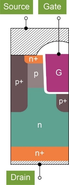
One of the primary goals of the CoolSiC MOSFET cell design was to limit the electric field in the gate oxide, both in the on- and off-states (Figure 4). Another goal was to provide an attractive specific on-state resistance for the 1200V class, achievable even in mass production. Sufficiently high gate-source-threshold voltages (4.5V typically), combined with voltage levels of only VGS = 15V, mean that a low on-state resistance is ensured. These values are benchmarks in the landscape of SiC transistors.
A self-aligning process orients the channel at a single crystallographic orientation, ensuring the highest channel mobility and narrowing the threshold voltage distributions. Another feature is the deep p-trenches intersecting the actual MOS trench in the center, to allow narrow p+ to p+ pitch sizes for effective screening of the lower oxide corner. The CoolSiC MOSFET also offers the ability to turn off the device with zero gate bias, making it a true “normally-off” device.
Figure 4: Sketch of the CoolSiC MOSFET cell structure
Source:https://www.infineon.com/dgdl/Infineon-High-performance_CoolSiC_MOSFET_technology_with_silicon-like_reliability-Whitepaper-v01_00-EN.pdf?fileId=5546d4626f229553016f8f5c95f02c54&da=t
The AIMW120R080M1 CoolSiC Trench 1200V MOSFET from Infineon Technologies was developed for the onboard charger and DC-DC applications in hybrid and electric vehicles. It features ultra-low switching losses, low RDS(on) (80 mohm), and an operating temperature range between -55oC to 175oC. Further features include the lowest gate charge and device capacitances levels, no reverse recovery losses, temperature-independent low switching losses, and threshold-free on-state characteristics.
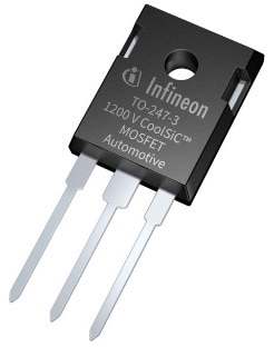
Figure 5: Infineon AIMW120R080M1 CoolSiC 1200V MOSFET
The IMBG120R090M1H CoolSiC 1200V MOSFET is available in a D2PAK-7L (TO-263-7) package built on a state-of-the-art trench semiconductor process optimized to combine performance with reliability in operation. It features ultra-low switching losses, short-circuit withstand time of 3 µs, low RDS(on) (90 mohm), XT interconnection technology to enhance thermal performance, and an additional sense pin for optimized switching performance. The low power losses of CoolSiC
technology, combined with XT interconnection technology, enable top efficiency and passive cooling potential for applications such as drives, chargers, and industrial power supplies.
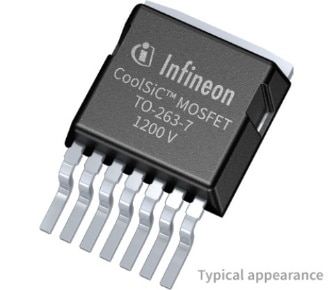
Figure 6: Infineon IMBG120R090M1H CoolSiC 1200V MOSFET
Summing Up: Designing MOSFETs with SiC
The outstanding material properties of SiC have enabled the design of efficient, fast-switching unipolar devices, such as the SiC MOSFET. The results are less heat dissipation, space savings, lower cost, and increased reliability. SiC MOSFETs are now poised to replace traditional transistors in a variety of applications, including electric and driverless vehicles with onboard charging units, space and military systems, solar power inverters, wind turbines, and more.
Infineon Technologies CoolSiC 1200V SiC Trench MOSFETs combine the strong physical characteristics of SiC with unique features that increase the device's performance, robustness, and ease of use. Suitable for high temperature and harsh environment operations, these devices enable the simplified and cost-effective deployment of highly efficient systems.

