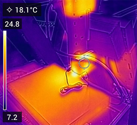
Modern electronic devices are replete with sensors that enable them to understand the environment in which they operate. Depending on the application of the electronic system, the sensors deployed can vary. They could include image sensors to capture images or videos, accelerometers and gyroscopes to track motion, or temperature and pressure sensors to understand the environment. Each system may contain more than one sensor type. You might have an image sensor capturing video in the visible band, for example, and a thermal or night vision sensor for use in low light conditions.
Individually, each sensor provides the user with significant information, but even more information can be obtained by fusing together the relevant information from each sensor. This sensor fusion allows for an enhanced situational understanding and perception.

One example of sensor fusion might be in industrial machinery. An industrial robot could be monitored with a variety of sensors; a temperature sensor to make sure it is operating at safe temperatures, a vibration sensor to detect abnormal motor movements, and a microphone to detect any abnormal mechanical sounds. Individually, each sensor provides very useful information, however, combining the three provides additional insight, potentially increasing the accuracy of any predictions or estimates.
By its very nature, sensor fusion is computationally intensive, because it needs to be able to interface with a range of sensors in parallel and perform the necessary calculations to create the sensor-fused solution. This presents several challenges to developers of sensor-fused solutions, including how they interface with the required number of sensors, and how they perform the computation required for the fusion in an energy efficient manner, while keeping the cost of the solution within budget.
AMD-Xilinx Spartan-7 FPGA
Cost-optimized FPGAs such as the Spartan-7 from AMD-Xilinx provides developers with the ability to leverage the flexible I/O provided by FPGAs in order to implement as many sensor interfaces as required. This frees developers from the constraints that can be associated with traditional microprocessor interfacing. The flexible structure of the programmable logic containing configurable logic blocks, block RAMs and DSP elements can be leveraged to achieve the parallel processing and fusion required in a power-efficient manner.
Like most FPGAs, the Spartan-7 is available in a range of devices that offer an increasing capability of CLB, BRAM, DSP, and IO.

At 28 nm, the Spartan-7 is the replacement for the very popular 45 nm Spartan-6 family. While both Spartan-6 and Spartan-7 devices provide the user with a six-input look up table, there are several advantages the Spartan-7 has over the older Spartan-6 FPGAs including:
- Spartan-6 block RAMs are arranged as 18 Kb blocks which can be configured as two 9 Kb memories. In comparison, the 7-series devices provide 36 Kb blocks that can be configured as two 18 Kb memories.
- Both Spartan-6 and Spartan-7 provide dedicated DSP elements that enable the developer to implement multiply-accumulate functions. The Spartan-6 device includes a DSP48A1, which provides 18x18 signed multiplication, while 7-series devices provide DSP48E1 which implements a 25x18 signed multiply. Architecturally, the DSP48E1 that is provided in 7-series devices also enables the implementation of an Algorithmic Logic Unit (ALU) and support of Single Instruction Multiple Data (SIMD) mode which allows increased throughput. The DSP48E1 is also capable of implementing pattern detection and 17-bit shifter structures as required by the application.
- The clocking architecture of 7-series devices is significantly simpler than what was previously provided in Spartan-6 devices. The Spartan-6’s clocking architecture has different buffer types that determine connections and connectivity, for example, BUFG, BUFH, and BUFIO2 or BUFPLL. Resource-wise, the Spartan-6 device provides Digital Clock Managers (DCM) and Phase Locked Loops (PLL) clocking resources. AMD-Xilinx 7-series devices provide the user with a simpler clocking architecture, which, along with flexibility, provides a significant improvement in performance. Clock Management Tile (CMT), MMCM and PLLs are also provided and associated with each I/O bank within 7-series devices.
- Both Spartan-6 and 7-series devices provide the user with the ability to interface with high-performance external DDR memory. The Spartan-6 device implementation uses an integrated memory block, whereas 7-series devices use a Soft IP core to implement the memory controller where only the memory PHY is hardened. This provides 7-series devices with a more flexible approach to I/O allocation and design, which can be critical when working with complex PCB designs. The 7-series memory interface controller can support DDR3, DDR3L, DDR2, and LPDDR2, which provides maximum flexibility when selecting the memory.
- The 7-series range also has new features that provide benefits to the developer. The first of these is the XADC, which is a 1 MSPS (Mega samples per second) ADC that enables the developer to observe the internal supply voltages and die temperature. This can be very useful when implementing self-test and anti-tamper features. The XADC is also able to quantize 16 external differential signals, removing the need for additional low-speed ADCs used in board monitoring. Along with the ability to provide bitstream security, the XADC is also enhanced with the provision of AES256 CBC encryption and SHA-256 authentication.
The major change between Spartan-6 and 7-series implementations is the tool chain used for development and implementation. Spartan-6 devices use the ISE, EDK, PlanAhead, and SDK tool chain while 7-series devices use the Vivado and Vitis tool chains. Vivado is a quantum leap in capability compared to the older ISE tool chain. Vivado enables developers to work with pure RTL designs and leverage a large built-in IP library using IP Integrator. IP Integrator is ideal for creating embedded system designs that contain processors within either the processing system of a heterogeneous system-on-chip or softcore implemented in logic such as MicroBlaze. Vivado provides developers with end-to-end capability and includes synthesis, place and route, bit generation, and hardware programming and debugging. Embedded software development takes place within Vitis, which is an Eclipse-based software development environment.
Speeding up Development and Testing
When it comes to creating sensor fusion applications, development boards provide a platform that can be quickly and easily used to demonstrate sensor fusion applications, thereby reducing the technical risk and increasing the technology readiness level of the application.
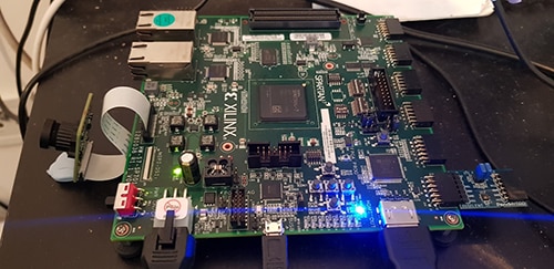
One of the most flexible Spartan-7 development boards is the SP701. This system provides developers with the largest 7-series device, dual Ethernet, 256 MB of DDR3L, MIPI camera interface, and MIPI display interface. In addition to providing a range of sensor interfacing options, the SP701 also features a low pin count FMC (FPGA Mezzanine Card) and] 6 Pmod interfaces. This enables image sensors to be connected via MIPI or the FMC connector, Time Sensitive Networking to be implemented using the dual Ethernet interfaces, and low-speed sensor interfaces implemented via the Pmod. The 256 MB of DDR3L also enables users to buffer data and allows the application to run the software application using a softcore MicroBlaze as necessary.
|
What is MIPI? MIPI is a high-bandwidth protocol for transferring image sensor or display information over several differential serial lanes. The MIPI Display Serial Interface (DSI) is the specification for the high-speed interface between a host processor and display module. The MIPI DSI is used in a wide range of devices, including smartphones and tablets, laptops, automotive displays, wearables, and virtual/augmented reality applications.
What does MIPI stand for? In 2003, when the MIPI Alliance was created, MIPI stood for “Mobile Industry Processor Interface”. Currently, the organization supports specifications for not only the processor, but the full range of connectivity needed in a device; therefore, the phrase was dropped and MIPI is no longer an acronym. |
Applications: Heads-up Display

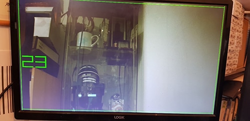
One example of sensor fusion on the SP701 is to create a simple heads up display that projects user information superimposed on the display. In this case, the SP701 can use its MIPI camera input and either HDMI or DSI output, while the sensor information to be displayed is received via the Pmod connector. The project uses several Xilinx IP cores, including MIPI CSI2 to receive the MIPI images, custom HLS IP cores to generate the HUD overlay with sensor data, video muxer to mix video streams from the MIPI input, and HD input to create the fused image. Controlling this application is a MicroBlaze processor that configures the image processing out and gathers the sensor data that will be output to the HUD element.

Development is done within Vivado Design Suite, Vitis, and Vivado Design Suite – HLS Edition. For this example application, coding is not required; the majority of the tasks involve setup and configuration of the hardware and built-in algorithms. Complete step-by-step instructions for the project can be found here.
Wrapping Up: Sensor Fusion with FPGAs and the SP701 Development Boards
Sensor fusion applications enable users to understand the operating environment beyond what can be gained from a single sensor. Cost-optimized FPGAs such as the Spartan-7 and development boards like the SP701 enable developers to create sensor fusion applications from the beginning of the project, helping significantly reduce the technical risk.
