


The Zynq family has an on-board 12 bit ADC, in the FPGA part of the silicon. They call it the XADC.
It can sample internal rails and temperatures. There's also the possibility to use external inputs.
In this series of 2 blogs, I'm trying to sample the ADC at high speed and move the samples to memory fast.
The goal is to achieve the highest speed - 1 MSPS (Megasamples per second = millions of samples per second).
In this first article, it's bare metal: write the Vivado hardware design and create a ARM program (C, running bare metal ARM A9) to look at the results.
Like many posts in my Zynq/PYNQ series, I'm using code and work of someone else. In this case a Hackster.io article by Adam Taylor.

Tools used:
- Zynq-Z2. For this first post, no PYNQ or SD card needed
- Vivado 2020.2
- Vitis 2020.2
- A variable supply, limited to max 1 V and optionally a voltmeter. The input range for the XADC is 0 V -> 1 V.
Reader beware: the technologies used here are all Xilinx and Zynq specific. This isn't portable.
Hardware Design in Vivado
This is a flow with a Xilinx XADC IP, and DMA/interface blocks surrounding it to manage that the samples arrive in the DRAM.
I've followed Adam's post. I'll try to show the configuration parts of the design.

click to enlarge
Processor, reset, clock
The clock for the FPGA isn't defined by the processor block this time.
The hardware needs to run at 104 MHz to achieve the maximum speed of 1 MSPS - there is overhead inside the XADC IP to exchange results.
This speed can't be generated with that precision in the processing system. The design adds a clock wizard to deliver that 104 MHz clock.

Processing System:
Place the Zynq IP and run the block automation.
Then, enable General Purpose Master AXI, High Performace Slave AXI, 100 MHz FPGA clock and interrupt


click to enlarge
Clock Wizard:
Add a Clocking Wizard IP, Set the frequency to 104 MHz, and alter the reset polarity.

Reset:
This block doesn't need customisation. All is good as is.
The Clock Wizard is the only block that gets the clock from the PS.
The Clock Wizard and Reset block are the only ones that get their reset from the PS.
All other blocks get the clock from the Clock Wizard and the resets from the Reset IP.
Adam uses the connection automation a few times in the article. I put all connections manually. The automation didn't behave as explained in that post.
I'm doing that methodically. I make all possible connections with the blocks available each time I add an IP. At the end, I revisit each block and complete all connections for them.
ADC Stream

click to enlarge
The ADC IP is surrounded by a number of AXI and DMA constructs to manage the transfer of sampled data to DRAM.
Most blocks, we've seen in previous posts in the Zynq series. There is one newcomer: the Stream Subset Converter.
The DMA process requires that there is an end signal to a data stream, in order to kick off a transfer to memory.
The XADC IP doesn't produce an end signal. It streams continuously.
The Subset Converter generates an end signal for us, when the XADC has streamed exactly the amount of samples to fill our DMA buffer. More on that later.
XADC Wizard:


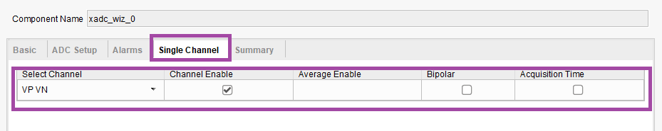
As mentioned before, the frequency is 104 MHz:
From Adam's article:
To achieve a sampling rate of 1000 ksps we need to set the DClk to 104 MHz as the XADC internally take 4 clock cycles for acquisition and 26 cycles for conversion
Stream Subset Converter
The DMA that we'll use later, will have a 256 byte buffer. The 12 bit ADC uses 2 bytes per sample.
That means our buffer will be full after 128 samples. We need to signal the DMA to send off our data to DRAM then. The XADC doesn't do that for us.
The Stream Subset Converter will do that. It'll nicely generate set AXI TLAST when that point is reached. Each time that it is reached.

You'll see that some of the default setting aren't matching when you open this dialog the first time.
Don't worry. The automatic settings will adapt to the correct state once you wired up the design and did a first validation.
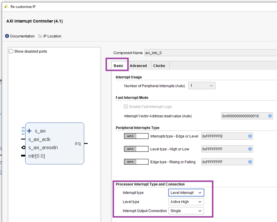
DMA and Interrupt Handling:

The DMA block gets the stream from the XADC, including the end-of-buffer signal. It uses an interrupt to notify ARM that the data is available.

There is no high speed data coming from the ARM, so we only enable the Write channel.
The automatic values will again adapt to the design at validation time.
AXI Interconnects
This image gives another perspective of the whole data flow, including the AXI Interconnects to manage the control channel (General Purpose AXI) and DMA (High Performance AXI).
I've shuffled the pin placements to untangle connections. The interconnect at the top manages the high performance data stream. The one at left handles the general control streams.
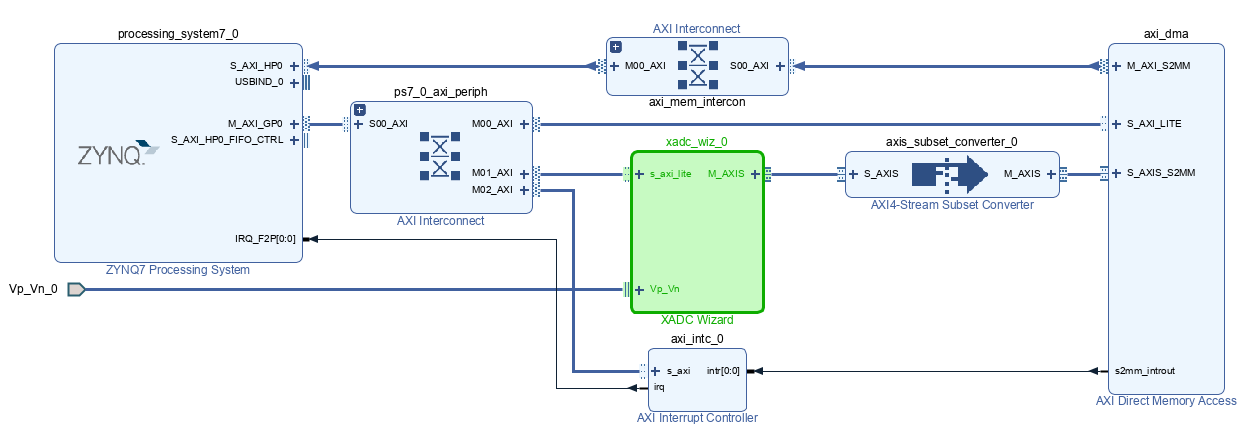
The General Purpose AXI Interconnect for the control signals needs 3 master interfaces. It controls 3 AXI blocks that need control signals to operate well together and with the ARM.
The one that controls the DMA needs 1 master interface.
Logic Analyzers
Adam added two logic analyzer IPs to the block design. One at the XADC stream output and one at the Subset Converter. They can be used for debugging or in the PYNQ notebooks.

Set both to protocol AXI4S

Wiring and Memory Map Allocation
Check the first diagram at the begin of this post for all connections. Be precise and complete.
Make the Vp_Vn input of the XADC external. You don't need to map this in the constraint file, because Vp and Vn go to a dedicated balanced analogue input.
The pins are available on connector J5. I'm using it unbalanced, with Vn tied to ground and Vp to the voltage I want to sample (max 1 V!).

image source: PYNQ-Z2 User Manual
Generate and Export Hardware
Validate the design, and generate the bitstream. Vivado will do all prerequisite for you. Grab a coffee.
Then export this hardware design. We'll use it in the next step to build a C program that can see the samples.
Bare Metal Test Bed in Vitis
In the next post, we'll use PYNQ and Python to get at the samples. Here, we'll use Adam's example program that runs on the ARM A9. No OS or SD card involved.
We'll use a Vitis (Eclipse) debug session to watch what's happening.
Prepare the board for Bare Metal access over JTAG and USB
On the PYNQ-Z2, I do that by moving jumper JP1 to the right, connect a standard USB cable between development PC and the PYNQ-Z2, then start.
You can leave the SD and network cable in place or remove them from the board. They are not used.
Check your board's manual.

image source: PYNQ-Z2 User Manual
Create a Vitis Project
In this step, you use the hardware design exported from Vivado, and create a project based on it.
Vitis will then know what microcontrollers are available and can be programmed/debugged. It also knows the peripherals we designed (E.g.: the XADC).
Adam has documented this step so detailed, that I can't add detail to it.
There is one error in the code formatted on Hackster. Line 76 has undesired blanks in the middle of a macro.
I'm replicating part of the code here, with that line fixed. It's also a part worth reviewing, because this is where the samples are retrieved from the memory map, after the DMA has transferred it.
	while(1){
		Status = XAxiDma_SimpleTransfer(&AxiDma,(UINTPTR)RX_BUFFER_BASE,MAX_PKT_LEN, XAXIDMA_DEVICE_TO_DMA);
		if (Status != XST_SUCCESS) {
			printf("XFER failed %d\r\n", Status);
			return XST_FAILURE;
		}
		while ((XAxiDma_Busy(&AxiDma,XAXIDMA_DEVICE_TO_DMA))){
			/* Wait */
		}
		Xil_DCacheFlushRange((UINTPTR)RxBufferPtr, MAX_PKT_LEN);
	}
code source: Adam Taylor's blog. I deliberately took a snippet. The blog has a complete listing.
Build the application using your Eclipse skills.
Load Bitfile and Debug the Application
In Vitis (and also in Vivado), you can directly load the bitfile over USB. We've enabled the board's JTAG-over-USB mode and that's what will be used by Vitis to perform the next actions.
First, we load the hardware design to the Zynq. That's via the Xilinx -> Program Device menu option.
Vitis knows where the bitfile sits in the export you did from Vivado. It 'll load and activate it.
At this point, ARM, XADC and the whole harness around them are operational. We can:
Program and Debug the Application

Your application will be loaded into the ARM memory, started, and the debugger halts it at the first executable line of source code in main().
This looks a lot like you'd use Eclipse for a microcontroller.
I've set a breakpoint so that we can have a look at the memory map that holds the 2 byte values of 128 measurements.
I'm using the memory monitor here to look at the raw memory. I could also have used a Watch Expression and display them as an array of unsigned integer.
Here is a view when sampling a 9.231 mV input signal:

Note that the values become available after you stepped over the breakpoint. I could set a breakpoint on the next line but there wasn't any next line in that loop :).
And when the input is 100 mV. This time I added an expression to look at the buffer as individual values (should have chosen u16):

That's it for part 1. Next article shows this in PYNQ and Python. Wih Linux OS.
Top Comments
-

Jan Cumps
-
Cancel
-
Vote Up
0
Vote Down
-
-
Sign in to reply
-
More
-
Cancel
Comment-

Jan Cumps
-
Cancel
-
Vote Up
0
Vote Down
-
-
Sign in to reply
-
More
-
Cancel
Children