element14 Community
element14 Community
    Register Log In
  • Site
  • Search
  • Log In Register
  • Members
    Members
    • Benefits of Membership
    • Achievement Levels
    • Members Area
    • Personal Blogs
    • Feedback and Support
    • What's New on element14
  • Learn
    Learn
    • Learning Center
    • eBooks
    • STEM Academy
    • Webinars, Training and Events
    • Learning Groups
  • Technologies
    Technologies
    • 3D Printing
    • FPGA
    • Industrial Automation
    • Internet of Things
    • Power & Energy
    • Sensors
    • Technology Groups
  • Challenges & Projects
    Challenges & Projects
    • Design Challenges
    • element14 presents
    • Project14
    • Arduino Projects
    • Raspberry Pi Projects
    • Project Groups
  • Products
    Products
    • Arduino
    • Dev Tools
    • Manufacturers
    • Raspberry Pi
    • RoadTests & Reviews
    • Avnet Boards Community
    • Product Groups
  • Store
    Store
    • Visit Your Store
    • Choose Another Store
      • Europe
      •  Austria (German)
      •  Belgium (Dutch, French)
      •  Bulgaria (Bulgarian)
      •  Czech Republic (Czech)
      •  Denmark (Danish)
      •  Estonia (Estonian)
      •  Finland (Finnish)
      •  France (French)
      •  Germany (German)
      •  Hungary (Hungarian)
      •  Ireland
      •  Israel
      •  Italy (Italian)
      •  Latvia (Latvian)
      •  
      •  Lithuania (Lithuanian)
      •  Netherlands (Dutch)
      •  Norway (Norwegian)
      •  Poland (Polish)
      •  Portugal (Portuguese)
      •  Romania (Romanian)
      •  Russia (Russian)
      •  Slovakia (Slovak)
      •  Slovenia (Slovenian)
      •  Spain (Spanish)
      •  Sweden (Swedish)
      •  Switzerland(German, French)
      •  Turkey (Turkish)
      •  United Kingdom
      • Asia Pacific
      •  Australia
      •  China
      •  Hong Kong
      •  India
      •  Korea (Korean)
      •  Malaysia
      •  New Zealand
      •  Philippines
      •  Singapore
      •  Taiwan
      •  Thailand (Thai)
      • Americas
      •  Brazil (Portuguese)
      •  Canada
      •  Mexico (Spanish)
      •  United States
      Can't find the country/region you're looking for? Visit our export site or find a local distributor.
  • Translate
  • Profile
FPGA
  • Technologies
  • More
FPGA
Blog Learning Xilinx Zynq: use RAM design for Altera Cyclone on Vivado and PYNQ
  • Blog
  • Forum
  • Documents
  • Events
  • Members
  • Mentions
  • Sub-Groups
  • Tags
  • More
  • Cancel
  • New
FPGA requires membership for participation - click to join
Blog Post Actions
  • Subscribe by email
  • More
  • Cancel
  • Share
  • Subscribe by email
  • More
  • Cancel
Group Actions
  • Group RSS
  • More
  • Cancel
Engagement
  • Author Author: Jan Cumps
  • Date Created: 2 Aug 2021 5:03 PM Date Created
  • Views 1536 views
  • Likes 4 likes
  • Comments 3 comments
  • zynq
  • pinq
  • xilinx
  • fpga
  • vivado
  • vhdl
  • automated_test_applications
Related
Recommended

Learning Xilinx Zynq: use RAM design for Altera Cyclone on Vivado and PYNQ

Jan Cumps
Jan Cumps
2 Aug 2021

Store 1024 12 bit values in a VHDL RAM design, and automatically test it.


This post uses the VHDL RAM design of Michael Kellett on a Zynq. You can store data and read it back.

The design was done out of curiousity. To see how and when Block RAM slices are used. Check the discussions in the comments of MKs post.

Here, I just focus on how the exercise is done with Vivado, Zynq and Pynq.

If this blog proves anything, it's that HDL is very portable.


VHDL Memory component


VHDL source of the memory design is exactly the same as Michael's, except that his block holds 64 12 bit values, mine 1024.

That's why I changed:

  • the name from mem_inf_sp_64_12 to mem_inf_sp_1024_12
  • the address from STD_LOGIC_VECTOR(5 downto 0) to STD_LOGIC_VECTOR(9 downto 0). It has to fit the 1024 values instead of 64
  • the array of data from array (0 to 63) to array (0 to 1023)

Latest source on github: https://gist.github.com/jancumps/72f319d33200af69d823701005e9d9cb


ZYNQ integration between FPGA and ARM / Linux


These signals will come from the ARM / Linux side

  • we: write enable. I use a GPIO for that
  • en: enable. Also a GPIO
  • address: address to read from or write to the memory. 10 MSB of a AXI memory mapped register
  • data: data to write. 12 LSB of that same AXI memory mapped register.
  • the clock

When a read is requested, the FPGA will send this back to ARM / Linux:

  • data: the value present at address when a read is requested. 12 LSB of that same memory mapped register.


Block Design


I've kept it as simple as I could. Just enough to provide the interfaces described in the previous section.

I'm going to skip explaining the mechanics but will show the configs. Every technique has been used before in this blog series.
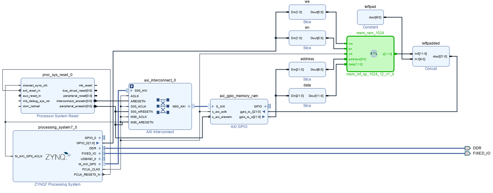
 

image

click to enlarge


The green block is Michael's Memory module. In the block design, I linked all inputs and outputs to the ARM / Linux interfaces.

For the technology used for each signal between ARM and fabric, see the section above.


Configuration


ARM


Zynq AXI for Data and Address register

image

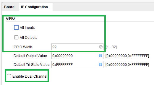
Zynq GPIO for Enable and Write Enable

image


Data and address (AXI)


AXI Interconnect

image


AXI GPIO

image

Address slice

Isolates the 10 Address bits out of a 32 bit AXI memory mapped register

image


Write Data slice

Isolates the 12 Data bits out of a 32 bit AXI memory mapped register

image


Read Data left-padded with 0

Concatenate (left pad) 10 '0' bits to the 12 data bits data, to fill all bits of the 22 bit wide AXI register

image

The constant 10 '0' bits

image


Enable and Write Enable (GPIO)


Enable slice

Isolates the Enable bit out of the 64 bit GPIO interface

image


Write Enable slice

Isolates the Write Enable bit out of the 64 bit GPIO interface

image


All of these blocks tie to the VHDL memory block. You'll see that the bit width and directions match.


Test Bed


I've tested the code in Python and Pynq.

The test loads a value to each memory location, and then automatically validates integrity.


Load bitstream


from pynq import Overlay
overlay = Overlay("memory_ram.bit")


Generate the GPIO API for Enable and Write Enable


# write enable and enable are GPIO pins
from pynq import GPIO
we = GPIO(GPIO.get_gpio_pin(0), 'out')
en = GPIO(GPIO.get_gpio_pin(1), 'out')

def disable():
    en.write(0)
    we.write(0)
    return
    
def write_enable():
    en.write(1)
    we.write(1)
    return

def read_enable():
    en.write(1)
    we.write(0)
    return


Generate the AXI API for Address and Data


from pynq import MMIO
memory_address = overlay.ip_dict['axi_gpio_memory_ram']['phys_addr']
RANGE = 4
memory_register = MMIO(memory_address, RANGE)

def memory_write(address, data):
    # must disable until register is set
    disable()
    # mask data for 12 bits maximum
    memory_register.write(0,address << 12 | (data & 0X0FFF))
    write_enable()
    disable()
    
def memory_read(address):
    # must disable until register is set
    disable()
    memory_register.write(0,address << 12)
    read_enable()
    data = memory_register.read()
    disable()
    return data


Execute unit tests


This section shows how you can fully automate the validation of a design.

This is useful while developing the FPGA blocks, but also as regression test when you change it.

Every address is filled with a value that can be checked later on.

For the tests, you can choose to test every address, or to spot check every so much positions. I'm testing every 128th address position.

The border conditions, the first and last memory address, are always tested.


address_count = 1024
test_granularity = 128
test_errors = 0

def change_data(data):
    return 2 * data

def test_data(address, data):
    success = (change_data(address) == data)
    if(success):
        print(f'memory at address {address:04}: OK')
        return True
    else:
        print(f'memory at address {address:04}: ERROR')
        return False

disable()

# fill all addresses with a different value 
print(f'fill all {address_count} addresses with a different value')
for i in range(0, address_count):
    memory_write(i, change_data(i))
    
print(f'validate every {test_granularity} address')

print('')
print('visual checks:')
print('==============')
# read a subset back
print('first read')
for i in range(0, address_count, test_granularity):
    print(f'memory at address {i:04}: {memory_read(i):04}')

print('second read to confirm read isn\'t destructive')
# check if no bogus writes
for i in range(0, address_count, test_granularity):
    print(f'memory at address {i:04}: {memory_read(i):04}')

print('')
print('unit test')
print('=========')
# check if data matches expectation
for i in range(0, address_count, test_granularity):
    if not (test_data(i,memory_read(i))):
        test_errors = test_errors + 1
                
print('test border cases first and last address always')
if not (test_data(0,memory_read(0))):
    test_errors = test_errors + 1
if not (test_data(address_count-1,memory_read(address_count-1))):
    test_errors = test_errors + 1
        
if test_errors > 0:
    print(f'test failed {test_errors} times')
else:
    print('all tests passed')


The test report:


fill all 1024 addresses with a different value

validate every 128 address


visual checks:

==============

first read

memory at address 0000: 0000

memory at address 0128: 0256

memory at address 0256: 0512

memory at address 0384: 0768

memory at address 0512: 1024

memory at address 0640: 1280

memory at address 0768: 1536

memory at address 0896: 1792

second read to confirm read isn't destructive

memory at address 0000: 0000

memory at address 0128: 0256

memory at address 0256: 0512

memory at address 0384: 0768

memory at address 0512: 1024

memory at address 0640: 1280

memory at address 0768: 1536

memory at address 0896: 1792


unit test

=========

memory at address 0000: OK

memory at address 0128: OK

memory at address 0256: OK

memory at address 0384: OK

memory at address 0512: OK

memory at address 0640: OK

memory at address 0768: OK

memory at address 0896: OK

test border cases first and last address always

memory at address 0000: OK

memory at address 1023: OK

all tests passed


The Vivado 2020.1 project and Jupyter code are attached.


Pynq - Zync - Vivado series
Add Pynq-Z2 board to Vivado
Learning Xilinx Zynq: port a Spartan 6 PWM example to Pynq
Learning Xilinx Zynq: use AXI with a VHDL example in Pynq
VHDL PWM generator with dead time: the design
Learning Xilinx Zynq: use AXI and MMIO with a VHDL example in Pynq
Learning Xilinx Zynq: port Rotary Decoder from Spartan 6 to Vivado and PYNQ
Learning Xilinx Zynq: FPGA based PWM generator with scroll wheel control
Learning Xilinx Zynq: use RAM design for Altera Cyclone on Vivado and PYNQ
Learning Xilinx Zynq: a Quadrature Oscillator - 2 implementations
Learning Xilinx Zynq: a Quadrature Oscillator - variable frequency
Learning Xilinx Zynq: Hardware Accelerated Software
Automate Repeatable Steps in Vivado
Learning Xilinx Zynq: Try to make my own Accelerated OpenCV Function - 1: Vitis HLS
Learning Xilinx Zynq: Try to make my own Accelerated OpenCV Function - 2: Vivado Block Design
Learning Xilinx Zynq: Logic Gates in Vivado
Learning Xilinx Zynq: Interrupt ARM from FPGA fabric
Learning Xilinx Zynq: reuse and combine components to build a multiplexer
PYNQ version 2.7 (Austin) is released
PYNQ and Zynq: the Vitis HLS Accelerator with DMA training - Part 1: Turn C++ code into an FPGA IP
PYNQ and Zynq: the Vitis HLS Accelerator with DMA training - Part 2: Add the Accelerated IP to a Vivado design
PYNQ and Zynq: the Vitis HLS Accelerator with DMA training - Part 3: Use the Hardware Accelerated Code in Software
PYNQ and Zynq: the Vitis HLS Accelerator with DMA training - Deep Dive: the data streams between Accelerator IP and ARM processors
Use the ZYNQ XADC with DMA part 1: bare metal
Use the ZYNQ XADC with DMA part 2: get and show samples in PYNQ
VHDL: Convert a Fixed Module into a Generic Module for Reuse


Attachments:
memory_ram.zip
memory_ram_jupyter.zip
  • Sign in to reply
  • Jan Cumps
    Jan Cumps over 1 year ago in reply to Jan Cumps

    ... first, as preparation: VHDL: Convert a Fixed Module into a Generic Module for Reuse.

    adapting the design so that I can make any size of memory with the same implementation.

    • Cancel
    • Vote Up 0 Vote Down
    • Sign in to reply
    • More
    • Cancel
  • Jan Cumps
    Jan Cumps over 1 year ago

    I'm going to try and adapt this example for DMA use, to exchange data between the RAM and the Zynq's DRAM.

    It could be a portability gateway. Vendor specific logic to get the RAM written and read from Compute side. Generic VHDL from RAM to other FPGA IP.

    • Cancel
    • Vote Up 0 Vote Down
    • Sign in to reply
    • More
    • Cancel
  • michaelkellett
    michaelkellett over 1 year ago

    Thanks Jan.

    When I get my Xilinx tools running and the board I'll attempt similar project on an Artix 35 chip.


    MK

    • Cancel
    • Vote Up 0 Vote Down
    • Sign in to reply
    • More
    • Cancel
element14 Community

element14 is the first online community specifically for engineers. Connect with your peers and get expert answers to your questions.

  • Members
  • Learn
  • Technologies
  • Challenges & Projects
  • Products
  • Store
  • About Us
  • Feedback & Support
  • FAQs
  • Terms of Use
  • Privacy Policy
  • Legal and Copyright Notices
  • Sitemap
  • Cookies

An Avnet Company © 2023 Premier Farnell Limited. All Rights Reserved.

Premier Farnell Ltd, registered in England and Wales (no 00876412), registered office: Farnell House, Forge Lane, Leeds LS12 2NE.

ICP 备案号 10220084.

Follow element14

  • Facebook
  • Twitter
  • linkedin
  • YouTube