element14 Community
element14 Community
    Register Log In
  • Site
  • Search
  • Log In Register
  • Community Hub
    Community Hub
    • What's New on element14
    • Feedback and Support
    • Benefits of Membership
    • Personal Blogs
    • Members Area
    • Achievement Levels
  • Learn
    Learn
    • Ask an Expert
    • eBooks
    • element14 presents
    • Learning Center
    • Tech Spotlight
    • STEM Academy
    • Webinars, Training and Events
    • Learning Groups
  • Technologies
    Technologies
    • 3D Printing
    • FPGA
    • Industrial Automation
    • Internet of Things
    • Power & Energy
    • Sensors
    • Technology Groups
  • Challenges & Projects
    Challenges & Projects
    • Design Challenges
    • element14 presents Projects
    • Project14
    • Arduino Projects
    • Raspberry Pi Projects
    • Project Groups
  • Products
    Products
    • Arduino
    • Avnet & Tria Boards Community
    • Dev Tools
    • Manufacturers
    • Multicomp Pro
    • Product Groups
    • Raspberry Pi
    • RoadTests & Reviews
  • About Us
    About the element14 Community
  • Store
    Store
    • Visit Your Store
    • Choose another store...
      • Europe
      •  Austria (German)
      •  Belgium (Dutch, French)
      •  Bulgaria (Bulgarian)
      •  Czech Republic (Czech)
      •  Denmark (Danish)
      •  Estonia (Estonian)
      •  Finland (Finnish)
      •  France (French)
      •  Germany (German)
      •  Hungary (Hungarian)
      •  Ireland
      •  Israel
      •  Italy (Italian)
      •  Latvia (Latvian)
      •  
      •  Lithuania (Lithuanian)
      •  Netherlands (Dutch)
      •  Norway (Norwegian)
      •  Poland (Polish)
      •  Portugal (Portuguese)
      •  Romania (Romanian)
      •  Russia (Russian)
      •  Slovakia (Slovak)
      •  Slovenia (Slovenian)
      •  Spain (Spanish)
      •  Sweden (Swedish)
      •  Switzerland(German, French)
      •  Turkey (Turkish)
      •  United Kingdom
      • Asia Pacific
      •  Australia
      •  China
      •  Hong Kong
      •  India
      •  Japan
      •  Korea (Korean)
      •  Malaysia
      •  New Zealand
      •  Philippines
      •  Singapore
      •  Taiwan
      •  Thailand (Thai)
      •  Vietnam
      • Americas
      •  Brazil (Portuguese)
      •  Canada
      •  Mexico (Spanish)
      •  United States
      Can't find the country/region you're looking for? Visit our export site or find a local distributor.
  • Translate
  • Profile
  • Settings
Test & Tools
  • Technologies
  • More
Test & Tools
Documents Programmable Electronic Load
  • Blog
  • Forum
  • Documents
  • Files
  • Members
  • Mentions
  • Sub-Groups
  • Tags
  • More
  • Cancel
  • New
Join Test & Tools to participate - click to join for free!
Actions
  • Share
  • More
  • Cancel
Engagement
  • Author Author: Jan Cumps
  • Date Created: 23 Dec 2016 1:09 PM Date Created
  • Last Updated Last Updated: 11 Oct 2020 8:05 AM
  • Views 19930 views
  • Likes 20 likes
  • Comments 401 comments
Related
Recommended

Programmable Electronic Load

Peter, Jon and Jan are building a programmable electronic load. This document is the common design sheet.

It's obviously work in progress. And fun.


image


We're building a programmable DC load. The focus is on making a real world working instrument.

Hardware and firmware are open source.

  • 20 V, 6 A
  • SCPI controlled


To keep this document readable, this main post gives an overview of the design.

All detailed explanations are broken out in separate posts.


Hardware

The load design is modular.


image


Two out of box modules:

  • MSP432 LaunchPad
  • LCD Shield (optional)

3 new designs

  • DAC-ADC module
  • Analog control module
  • Power module


DAC-ADC BoosterPack

image

This module is a generic, isolated DAC / ADC boosterpack. It's the interface between the analog controller and the microcontroller.

It can also be used outside this project, for your other analog - digital conversion needs.

The board design is broken out in a separate post: Programmable Electronic Load - DAC / ADC BoosterPack.


Analog Controller and Driver Board

This is the core of the analog constant current block. Here lives the circuit that will translate desired constant current into the driver signal for the power MOSFET.

It integrates the feedback coming from that power board. This is a closed analog control loop.

There are also components to provide the on-off functionality and buffers/amplifiers for the analog data-points that fly back to the ADC module.

image

The board, schematics and BOM are documented in Programmable Electronic Load - Analog Controller and Driver Board.


Power Module - the MOSFET Board with Fan


image


For details  of the design of the power stage, check Programmable Electronic Load - Power Stage.


BoosterPack Header Use and Pin Allocation

This info is broken out in a separate post: Programmable Electronic Load - BoosterPack Header Use.


Firmware


Prerequisites:

  • CCS 8 with MSP432 compiler TI v 16.12.0.STS or >
  • TI-RTOS for MSP43X, any SimpleLink version
  • MSP432 LaunchPad (not the black pre-prod because it's out of support)


The firmware is for the MSP432 microcontroller. But the harware can be driven from any controller, processor, PSoC or computer that can deliver i2c and power between 3V3 and 5V.

That includes Arduino, Raspberry Pi, BeagleBone, Warp7, IOT20xx, the ST Neo family, ... As long as they match that voltage range and have I2C master, it 'll work.

The ADC/DAC board takes care that the logic side is galvanicaly isolated from the power side (that is, if you leave the P1 and P2 jumpers open).


The only requirement is that you have a positive supply between 3V3 and 5V, a ground, and I2C signals (the board has I2C pull-ups that connect to the positive supply that you provide. If you don't want that (maybe your dev board already has 'm), leave R1 and R2 off.

ADC, DAC and Enable are all I2C driven.


GITHUB location: https://github.com/jancumps/msp432/tree/master/MSP432_SCPI_ElectronicLoad

download latest source files as a zip : https://github.com/jancumps/msp432/archive/master.zip

doxygen generated API documentation: https://jancumps.github.io/msp432

GIT artifacts don't contain CCS project files, only sources - get a zip with CCS project from the attachments at the end of this document.

image


SCPI interface and Error Handling

The SCPI commands are documented in this breakout post: SCPI interface.


UART Configuration

Together with SCPI, UART is the programming interface of this instrument.

The approach, and how to compile for USB or TTL, is documented in this breakout: UART.


RTOS and Posix Configuration

The TI-RTOS documentation is in breakout post RTOS Config.


LCD Display

Check here for a detailed explanation: LCD Display

The firmware supports SHARP LCD display,
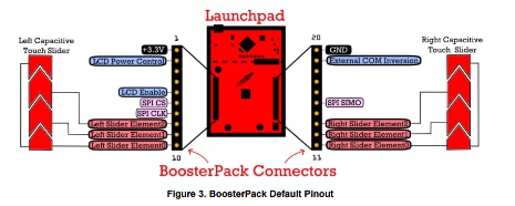


image

image


ADC


I've broken out the ADC description to a separate post, because I'm working on improvements:

Programmable Electronic Load - ADC Firmware


DAC


DAC output is set on command, using RTOS MailBox and messaging.

The payload for a DAC message contains the DAC channel that needs to be set, and the value.


typedef struct MsgDAC {
    uint8_t module;
    uint16_t value;
} MsgDAC;


The DAC task is started by RTOS. It inialises the DAC settings, then waits until it receives a message.


void *threadDAC(void *arg0) {


    MsgDAC d_msg;
    d_daci2cTransaction.writeBuf = d_dactxBuffer;
    d_daci2cTransaction.readBuf = d_dacrxBuffer;
    d_daci2cTransaction.slaveAddress = DAC_I2C_ADDR;
    d_daci2cTransaction.writeCount = 3;
    d_daci2cTransaction.readCount = 0;


    mqd_t mq;
    struct mq_attr attr;


    attr.mq_flags = 0;
    attr.mq_maxmsg = 1;
    attr.mq_msgsize = MSGDAC_SIZE;
    attr.mq_curmsgs = 0;
    mq = mq_open(QUEUE_NAME_DAC, O_CREAT | O_RDONLY, 0644, &attr);


    while (1) {
        ssize_t bytes_read;
        bytes_read = mq_receive(mq, (char *)&d_msg, MSGDAC_SIZE, NULL);


        /* wait for mailbox to be posted by writer() */
        if (bytes_read) {
// ...


The waiting doesn't take processor time. RTOS takes care that it will only get a slice of clock cycles when there is a message.

Two things in the RTOS configuration make this happen:

The mailbox with room for exactly one message, and a receive event.


Because there is usually no message in the mailbox, the execution of the DAC logic becomes inactive at this line:


        bytes_read = mq_receive(mq, (char *)&d_msg, MSGDAC_SIZE, NULL);


When we send a DAC message somewhere else in the code (e.g.: when the user requests a new setting of the electronic load), RTOS reactivates the process and hands over the payload message.

The DAC task sets the output of the requested channel and returns to the point where it waits for a new message.


   while (1) {
        ssize_t bytes_read;
        bytes_read = mq_receive(mq, (char *)&d_msg, MSGDAC_SIZE, NULL);


        /* wait for mailbox to be posted by writer() */
        if (bytes_read) {
            d_dactxBuffer[0] = getAddressFromModule(d_msg.module); // set value direct
            d_dactxBuffer[1] = d_msg.value >> 8; // MSB
            d_dactxBuffer[2] = d_msg.value; // LSB
            if (! I2C_transfer(i2c_implGetHandle(), &d_daci2cTransaction)) {
//                System_printf("I2C Bus fault\n");
//                System_flush();
            }
        }
    }


You select the DAC channel by setting bit 2 and 1 in the control byte (tx_buffer[0]). There's a helper function that gives a correct control record.


// address 7 - 6: 0, load mode 5 - 4: 01 direct from i2c, 3: reserved 0, 2 - 1: channel select, 0: pwr down 0
#define DAC857X_CFG_H0 0b00010000
#define DAC857X_CFG_H1 0b00010010
#define DAC857X_CFG_H2 0b00010100
#define DAC857X_CFG_H3 0b00010110


static const uint8_t array_DAC857X_CFG_H[4] = {DAC857X_CFG_H0, DAC857X_CFG_H1, DAC857X_CFG_H2, DAC857X_CFG_H3};

/**
 * get the hex address for the requested DAC module
 */
uint8_t getAddressFromModule(uint8_t module) {
    return array_DAC857X_CFG_H[module];
}


Bits 7 - 3 and 0 are all fixed.


image

image


Input Enable


The functionality to activate and deactivate the load is documented here: Programmable Electronic Load - Input Enable Functionality .


Control Strategies


The firmware uses strategies to handle the different types of load operation (e.g. constant current, constant, voltage, ...).


A strategy is a set of functions that you can plug in, and that together run that particular operation type (this is a c version of the Gang of Four's Strategy Design Pattern).

The goal is to avoid that the firmware is riddled with if or switch statements whenever different behaviour is needed depending on the instrument's mode.

Each operation strategy will have the same set of functions that run the instrument in that mode.

The price to pay is not expensive - speed and memory burden is low. It is a little more complex to understand than the c++ version. Once you step trough it with a debugger, things become clear.

The code also tries to hide that we're using strategies


Currently starting to implement constant current strategy. The more difficult operation types can be added later, one by one, with not too much impact on the existing code across the firmware.

. Only the eload API (see below) knows about it. All code goes via that eload API.

API for the stategies is minimal now:


    controlFunction;
    getMode;
    getChar;


eload API


The eload API offers an abstraction layer for the strategies, so that the rest of the firmware doesn't have to know about it. It simplifies switching operation mode and driving the instrument.


Example: The eload API offers a simple function eloadGetMode() to check what the instrument's current mode is.


eload_mode eloadGetMode() {

    return getControlStrategy()->getMode();

}


In the background, it uses the strategy mechanism to fetch the mode from the currently active strategy and call the implementation function.


return getControlStrategy()->getMode();


The eload API also has the common eload functions that don't need a strategy because they are always valid, regardless of mode.


Calibration and Configuration Data


The functionality to store calibration and configuration data in Flash is described in a separate article: Programmable Electronic Load - Calibration Data in Flash.

The calibration and configuration procedures are documented in Programmable Electronic Load - Calibration Steps


Changes To Standard MSP_EXP432P401R.c


The standard file generated by the TI-RTOS application wizard has defaults for peripherals.

The following has changed: none - I removed this section because with the external ADC/DAC board and the SimpleLink RTOS version, everything is kept standard.


Remote Software


Teminal


Serial communication to the USB UART port.

9600/8/1/None

image

SCPI is a non-echoing protocol. To make the characters you type show in the Terminal, set Local echo to Force on.

If you also set Local line editing to Force on, you have the opportunity to correct characters in the current line before they are sent to the serial port.

image


Test:

*IDN?;SYST:ERR:COUN?

Should return

THEBREADBOARD,ELECTRONICLOAD,0,01.00;0


Windows GUI


There are two image. A .NET made by Peter, a Java version made by Jan.


The .net GUI supports reading the 4 ADCs, setting one of the DACs abd shoot any SCPI command.

There's a window for SCPI output and a status window that shows SCPI errors.

image

Source and binary available from https://github.com/thebreadboard/SCPI_DC_LOAD_WIN


You don't have permission to edit metadata of this video.
Edit media
x
image
Upload Preview
image


The Java GUI is made as a POC that cross-platform instrument GUIs are possible.

It allows for switching the load on and off, set constant current and replicate the LCD values.

Additionally, you can requesst error status and run arbitrary SCPI commands.

Programmable Electronic Load - Java GUI Part 1: Basic Functionality


image


LabVIEW


The instrument comes with a LabVIEW library: Programmable Electronic Load - Write a LabVIEW Library part 1: Initialise Block
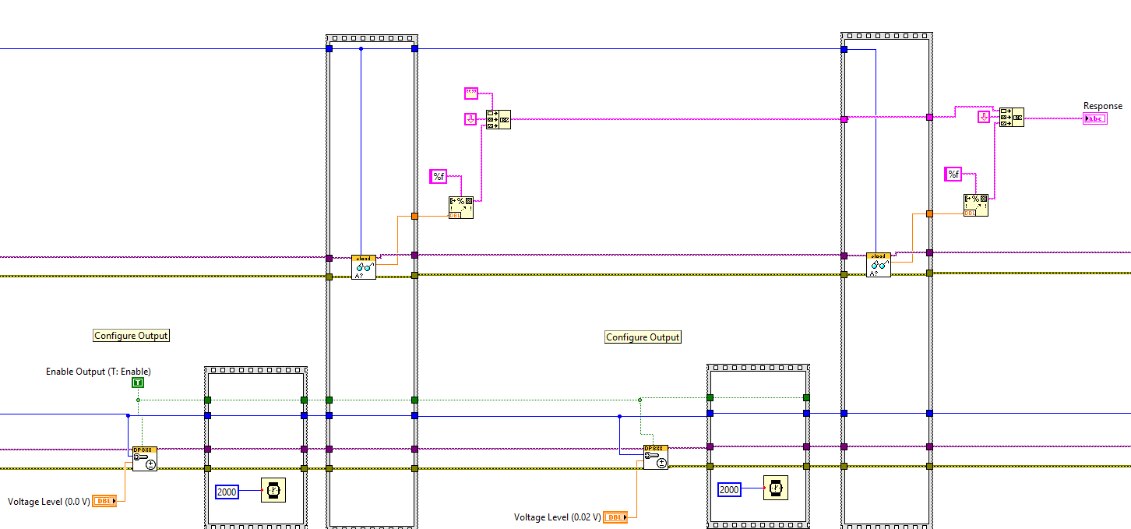
image


You don't have permission to edit metadata of this video.
Edit media
x
image
Upload Preview
image


Related blog

Programmable Electronic Load - Input Enable Functionality
Programmable Electronic Load - Power Stage
Programmable Electronic Load - Temperature Protection
Programmable Electronic Load - DAC / ADC BoosterPack
Programmable Electronic Load - Analog Controller and Driver Board
Programmable Electronic Load - SCPI interface and Error Handling
Programmable Electronic Load - UART
Programmable Electronic Load - RTOS Config
Programmable Electronic Load - Calibration Data in Flash
Programmable Electronic Load - Calibration Steps
Programmable Electronic Load - LCD Display
Programmable Electronic Load - ADC Firmware
Programmable Electronic Load - Current Sense Circuit
Programmable Electronic Load - BoosterPack Header Use
Programmable Electronic Load - ToDo and Done
Robert Peter Oakes articles:
Electronic DC Load - Design and Build to test PSU Project
youtube: Electronic DC Load Design and Testing
youtube: Full Build Analogue DC Load
youtube: Electronic DC Load - Performance Improvements
Raspberry PI 2, Fun with I2C DACs and ADC's
jc2048 articles:
Programmable Electronic Load: Dynamic Behaviour: Part 1 Overview
Programmable Electronic Load: Dynamic Behaviour: Part 2 The Servo Loop
Programmable Electronic Load: Dynamic Behaviour: Part 3 Effect of Output Inductance
Programmable Electronic Load: Dynamic Behaviour: Part 4 Effect of Output Voltage Change
Programmable Electronic Load: Dynamic Behaviour: Part 5 Stability
Programmable Load Build
Jan Cumps articles:
Programmable Electronic Load - ADC and DAC BoosterPack test
Programmable Electronic Load - Analyse the Summing Node Zero Point
Programmable Electronic Load - Measurements Part 1: Control Circuit
Java GUI
Programmable Electronic Load - Java GUI Part 1: Basic Functionality
Programmable Electronic Load - Java GUI Part 2: Support for Current Mode, Input On/Off, Error Log
LabView
Programmable Electronic Load - Write a LabVIEW Library part 1: Initialise Block
Programmable Electronic Load - Write a LabVIEW Library part 2: Read Output Block
Programmable Electronic Load - Write a LabVIEW Library part 3: Close Block
Programmable Electronic Load - Write a LabVIEW Library part 4: Function Set Block
Programmable Electronic Load - Write a LabVIEW Library part 5: Input Control Block
Programmable Electronic Load - Write a LabVIEW Library part 6: Raw DAC Block
Programmable Electronic Load - Write a LabVIEW Library part 7: Raw ADC Block
Programmable Electronic Load - Automating a DC Switcher Efficiency Test with LabVIEW
Programmable Electronic Load - LabVIEW Test Automation: Characterise the Instrument
Programmable Electronic Load - LabVIEW Test Automation: Characterise the Instrument Pt 2: Oscilloscope Measurements
Example LabVIEW Scenario: test a design with a Rigol PSU and a Keithley DMM
TI-RTOS: Switching to the SimpleLink Distribution
Switch from TI-RTOS to SimpleLink POSIX: Threads and Semaphores
Switch from TI-RTOS to SimpleLink POSIX: EEPROM API
Switch from TI-RTOS to SimpleLink POSIX: From MailBox to Message Queue
Switch from TI-RTOS to SimpleLink POSIX: LCD Display Driver
Switch from TI-RTOS to SimpleLink POSIX: Sleep when Idle
Attachments:
pcb_proto.zip
eload_v1_20170227.zip
eload_1_2a.zip
https://community.element14.com/cfs-file/__key/communityserver-wikis-components-files/00-00-00-00-21/bom.ods
MSP432_SCPI_ElectronicLoad_20180102.zip
eload_power_20180104.zip
eload.zip
eload_examples.zip
MSP432_SCPI_ElectronicLoad_20180514.zip
measureefficiency.zip
measureefficiency_5V_10V_600mA_RAW.zip
MSP432_SCPI_ElectronicLoad_v_00_0_0_1_20180914.zip
MSP432_SCPI_ElectronicLoad_20190706.zip
  • load_cell
  • metrology
  • msp432
  • ti-rtos
  • launchpad
  • laboratory
  • instrument
  • Share
  • History
  • More
  • Cancel
  • Sign in to reply

Top Comments

  • Jan Cumps
    Jan Cumps over 6 years ago +4
    Revisiting the eLoad design - there's definitely room for approval. The very low currency (minus 3 mA) is awful. And the calibration is off. I've set it to 0.5 A- and it thinks it's drawing that current…
  • Jan Cumps
    Jan Cumps over 8 years ago in reply to Jan Cumps +3
    All components are now in and soldered. Time to test. I'll first check out the power rails in isolation. If they are ok. I'll mount LaunchPad, LCD and and DAC board and do measurements. Hang on
  • Jan Cumps
    Jan Cumps over 8 years ago +3
    good news: I finally got persistent saving of calibration/setup sorted out. At first I had issues getting the in-ROM Flash api recognised by the compiler when using it with RTOS. That turned out to be…
  • Robert Peter Oakes
    Robert Peter Oakes over 8 years ago in reply to jc2048

    Forgot to also mention - re the summing junction. This is exactly the same as connecting the feedback 100K to the output of the op-amp (Making it a stand alone gain without the rest of the loop) and is how an inverting configured op-amp works, we have simply extended the feedback to include the sense resistor and the mosfet.

    • Cancel
    • Vote Up +2 Vote Down
    • Sign in to reply
    • More
    • Cancel
  • Robert Peter Oakes
    Robert Peter Oakes over 8 years ago in reply to jc2048

    Nice work there Jon


    A Lot of the solution I think would be in selecting the right Op-Amp, one with hi impedance inputs for instance.

    One of the reasons for selecting such high value resistors was to significantly reduce the chance of frying the electronics if something went wrong with the power stage, I have already fried the entire project with my old design because the common mode volts went way out of range (Up to the source voltage of 30V), the resultant current I think exceeded the input diode protection (10mA) and the rest was history image. So 100K with even 60-100V source to the load leads to a max of only 1mA flowing into the protection diodes, well within its safe current.


    So could we reduce the values. Yes of course but I would be tempted to stay well away from the 10mA max current in a failure mode (Or a simple spike getting through), so perhaps not less than about 20K = 5mA in fault condition.


    Hope this helps to understand my choices.


    Oh, the summing junction is just a very simple way of balancing setpoint with measured and if you make both resistors the same with the same characteristics then there always going to be the same sum even if they get hot etc. They should drift the same image. Also if it's good enough for Agilent, its good enough for me image and it keeps the component count small, especially for the silicon.

    • Cancel
    • Vote Up +1 Vote Down
    • Sign in to reply
    • More
    • Cancel
  • Robert Peter Oakes
    Robert Peter Oakes over 8 years ago

    Hi Folks, I have found some really good MOSFETS for the DC LOAD, there definitely not cheap but they avoid a lot of the issues f paralleling up mosfets and thermal runaway when running below Gate Threshold, I have two of the 17 pounds each one and one of the 30pound ones on their way to me. The nice thing is they have excelent mounting ability and also have specific ratings for DC conditions.

    they are

    IXYS IXFN140N30P N-channel MOSFET, 115A, 300 V HiperFET, Polar, 4-Pin SOT-227B  IXFN140N30P IXYS SEMICONDUCTOR, MOSFET Transistor...

    and

    IXYS IXTN46N50L N-channel MOSFET, 46 A,500 V Linear, 4-Pin SOT-227B 

    the first one is actually a switching MOSFET by design but does have a published rating for operation at DC (Most power mosfets are rated at the "Power" for only say a 10mS pulse or less), the second is truly designed for linear use (Designated by the "L" in the part number.

    Here is a cheaper alternative IXTX90N25L2 IXYS SEMICONDUCTOR, MOSFET Transistor...

    This is what I was looking for in the characteristics, note the inclusion of a DC components. Again, with the right heat sink, this could run over hundreds of Watts on its own. I would suggest using the higher temperature graphs as it would be more realistic.,

    image

    They will both easily run at 200W DC conditions (Way less than the dynamic pulse mode, one is rated at over 1KW in pulse mode), you will see in the spec sheets that they are down to 10A or so in the SAFE operating area for DC, but at almost the full voltage. A bit of cleaver programming can adjust the boundaries as the different voltages are detected, also if we add pulse mode then we could handle way more.

    This does not mean a constructor has to use these, but it's simply a simple and cool option, especially when in my case my other sponsor is sending me them :). Its all about building the power stage to meet your needs and budget. The control circuit should be abkle to handle quite a range of Mosfets with out change, capacitance on the gate may of course affect oscillations or response times but aside from that everything else should be good. It may be a week or so before I get them, but I just wanted to let you know.

    • Cancel
    • Vote Up +2 Vote Down
    • Sign in to reply
    • More
    • Cancel
  • jc2048
    jc2048 over 8 years ago

    Next I'm going to have a quick look at the stability of the original circuit.


    Remembering back to the things I learnt many years ago [I wasn't a very diligent student and didn't pay as much attention as I should have done], the

    necessary conditions for sustained oscillation in a circuit are that there should be feedback and, at some frequency,

    there should be gain of more than one (otherwise any oscillation will just die away) AND the signal fed back should

    reinforce and not counter the oscillation. Stability is more than just the absence of oscillation of course, but it's

    a good starting point and the tools that we use to look at it will give us some idea of how the circuit will behave

    generally (whether it will overshoot and ring if hit by a fast edge for instance). All of this was investigated by

    people back in the 1940s, the two most well known being Nyquist and Bode. Bode's method, derived from that of

    Nyquist, used separate gain and phase plots and was also useful where systems were measured (rather than the curves

    being pieced together from knowledge of how the individual circuit elements would behave theoretically). I'm going to

    try and see if I can get some Bode plots for this circuit using the simulator and then look at the effect that having

    some inductance in the test leads, used to connect the load to the circuit under test, might have. I haven't got a

    clue how you SHOULD do this [I was never taught anything about simulation], but other people do it so it can't be too

    difficult. [Just don't assume I know what I'm doing, that's all.]


    Here's the circuit I'm using:


    image

    What I'm doing is simply breaking the loop, feeding a signal in from a signal generator and recording the signal that

    finds its way all around the loop and back to the break point. I'm measuring the open-loop response rather than the

    closed-loop response. I've set the normal circuit input to a fixed value of 2V. By the way, that break in the loop

    can occur anywhere around the loop. That seems a bit odd at first but, if you think about it, wherever it is that you

    break the loop, one complete circuit round has to have the same effect. The break must be in the actual loop, though,

    whether it's in the forward path or the fed back path.


    There's a complication with this circuit, though. The feedback sets the operating point for the MOSFET. With the loop

    broken, it won't find the correct operating point and I'll probably just be sending a small signal round the loop

    through the gate-source capacitance and the results will be wrong because I'll be measuring something different to

    what the real circuit does. So, what I did was to get the simulator to analyse the dc nodal voltages with the loop

    intact, read the voltage at the end of the diode where I'm going to attach the signal generator, and then I added

    that voltage as a dc offset to the signal generator so that the small sinewave it uses to do the frequency analysis

    was swinging around that operating point. [I imagine that there's some clever way to get the simulator to do that for

    itself, if only I knew what it was - I couldn't think of anything that wouldn't upset the results.]


    Here are the plots of gain and phase for the circuit with no added inductance on the output.


    image

    image

    We can derive two figures from these plots that give us some measure of how far we are from oscillation. The phase

    margin is how close the phase gets to zero degrees (or +-360, depending how the simulator likes to give it to us on

    the plot) before the gain gets down to unity (0dB). The gain margin is how far the gain is below 0dB when the phase

    gets to zero degrees. People sometimes define the phase margin as being the value when we get to unity gain. I think

    that comes from considering the simpler situation of amplifiers where the gain and phase will often both decline

    nicely at higher frequencies and the worst case for the phase is then the same point as the gain falling to unity.

    With something like this, where the output load has a major effect on how the loop performs (the output load isn't

    inside the loop, but the current through it also flows through the current sense resistor which is), we're rapidly

    moving away from a simple textbook example.


    I've drawn these onto the plots with a paint package. The phase margin is 90 degrees and the gain margin is 34dB.

    They are both very safe. People seem to have different ideas about what constitutes an adequate gain and phase

    margin. Integrated Electronics (Millman and Halkias, 1972) says 'a linear amplifier of good stability requires gain

    and phase margins of at least 10dB and 50 degrees respectively'. Other books I've read suggest 30 degrees is

    sufficient for control systems. The complication is that we are just looking here at one aspect of how the control

    loop behaves and there are other criteria to look at too. For instance, we may want to trade some stability for

    better agility and a faster response (one immediate observation we can make of the gain plot is that the loop runs

    out of gain at 23kHz - that means there's no possibility of oscillation further up, but the load isn't going to be

    doing very much either).


    Here is the same test again, but this time with two test leads each having 1.4uH of inductance. (That's one metre of

    1.6mm [14 AWG] diameter wire with no coupling between the leads - in practice there would be some mutual coupling

    where the leads come together at the load and at the circuit being tested, even if you spaced them as far apart as

    possible in between.)


    image


    image

    image


    This time the phase margin is just 23 degrees and the gain margin is 13dB. Although it's still stable [in the sense

    of not oscillating], the much lower phase margin means that it may overshoot and ring on a fast edge. [What would be

    interesting here would be for me to try a range of different inductances to get a feel for how the two plots vary.

    I'll have a go at that over the weekend if I've got time.]


    Remember that this is the result of a simulator running, so it's only as good as the models and I wouldn't expect it

    to be totally accurate, particularly as the frequency goes up and parasitic capacitances come into play. In any case

    the models will be using typical figures (or perhaps worst case 25C figures for the leakages and bias currents?) so

    there will be more variation there. Also, I substituted an alternative part for the MOSFET that Peter originally had

    and the internal capacitances between the terminals will be different. So this is all a bit rough and ready - it

    helps us understand and is a guide to what the circuit would do but it isn't reality. The other point to remember is

    that this is the small-signal performance - things will be different for large signals where op-amp slew rate comes

    into play and there is also the possibility that signals will distort.


    Edited 12th June 2017: I pasted in the wrong circuit and curves for the case with lead inductance (I had the 1mH ones,

    and they should have been the 1.4uH ones) - I've just replaced them.

    • Cancel
    • Vote Up +1 Vote Down
    • Sign in to reply
    • More
    • Cancel
  • jc2048
    jc2048 over 8 years ago in reply to Jan Cumps

    image

    Bribe has arrived. Thank you Jan.

    • Cancel
    • Vote Up +2 Vote Down
    • Sign in to reply
    • More
    • Cancel
  • Jan Cumps
    Jan Cumps over 8 years ago in reply to jc2048

    correction: 2 adc/dac pcbs image

    • Cancel
    • Vote Up +1 Vote Down
    • Sign in to reply
    • More
    • Cancel
  • jc2048
    jc2048 over 8 years ago

    I'm back again, after a bit of shameless bribery from Jan (I get one of his spare ADC/DAC booster boards in return for some more thoughts and comments).


    I'm interested in how the control loop works: why there's such a large offset at the bottom end of the current range (and what can be done about it) and what the advantages are (if any) of the summing arrangement (which I'm not familiar with at all).


    I don't have much of a background in analogue design, so I'm learning this as I go along. (Please shout if you see me getting things wrong.)


    Input Bias


    Here's the control loop in a simplified form so that it's easier to see the control action. (I've stripped away all the frequency dependent stuff, so we're looking at dc here - keep in mind that there will be other complications at ac.)


    image


    Here's how I see the control operating. The control input is a positive voltage in proportion to the desired current. The signal fed back by the current sense amplifier is a negative voltage (it's negative because the gain is -7.8, not 7.8). The op amp acts to try and make both of its inputs the same voltage, so with the two resistors the same value, the fed back voltage will match the control voltage, except for its sign. If the control were set to 1.95V, the opamp would control the MOSFET to give 5A through the sense resistor so that the fed back voltage were -1.95V and the voltage at the + input to the opamp was then 0V.


    Now, what is the current through the pair of resistors for different input voltages? Let's pretend for a moment that the opamp is perfect and doesn't load the midpoint at all.


    Input voltage    % of full scale    Desired Current    Resistor Current
    1.95                 100                      5A                       19.5uA
    195mV             10                       500mA                1.95uA
    19.5mV             1                       50mA                   195nA
    1.95mV             0.1                    5mA                     19.5nA


    That seems fine (perhaps 'fine' isn't the word - it seems to me to be a fundamental flaw of the arrangement the way the control current falls off for low control voltages - maybe a doubtful 'plausible' or 'possible' might be better) until we look at the datasheet for the opamp and see this


    image


    In case it's not clear why the current is negative (flowing out of the chip), here's the equivalent schematic from the datasheet where we can see that the input transistors are PNP


    image


    The Input Bias Current that flows out of the bases of the transistors is typically -0.7uA [for supplies of +-15V]. If we compare that to the current through the two resistors, we can immediately see that there is going to be a problem at the lower end of the input control voltage range where the bias current is much higher than the current through the resistors.


    Can the circuit be improved? My first thoughts on that would include the following.


    One option would be to decrease the size of the resistors. If we made them 10k, rather than 100k, the resistor currents would be ten times higher. That would help a bit. How far could we go with that? It looks like the current sense amplifier can drive 1k or 2k sensibly. I don't know about the DAC.


    Another thing we could do is to be very rigorous about balancing the inputs to the opamps. Whilst the bias current is fairly high, both inputs will match well [the transistors will be almost identical being fabbed on the same piece of silicon] and the currents tend to cancel if we can make the resistance looking out of the terminal the same for both the input pins. A problem there, though, is the frequency selective network feeding back locally around the opamp - what frequency do we make the inputs balance for? It has to be DC, but then it's going to change as the frequency goes up.


    A more obvious option would be to substitute an op-amp with a lower input bias current. There are bipolar op-amps with much lower bias currents (they include extra circuitry to offset the current internally), MOSFET-input op-amps have an input bias current in the pA area [mostly the protection diode leakage], and FET inputs are almost as good. However it's complicated by temperature [leakage currents climb quickly with increased temperature], so substituting an op-amp is a bit more complicated than just choosing on the basis of one parameter (and we may just be swapping one problem for another).


    There's also the question of whether it's good to stick with the summing junction approach.


    Before considering that any further, I'm going to see if I can look at the stability and the frequency response of the current circuit - partly to find out how to do it, partly to understand what bearing the summing arrangement has on the stability, and also because I want to see what effect output loads have and what a reasonable spec might be for such an instrument.

    • Cancel
    • Vote Up +1 Vote Down
    • Sign in to reply
    • More
    • Cancel
  • Robert Peter Oakes
    Robert Peter Oakes over 9 years ago in reply to jc2048

    The gain is selected in part to use absolute standard resistors, no trim pots etc, and 7.8 was close enough to the max Ref voltage to be suitable and leave a little room for detecting over voltage, use for AutoRange via the PGA or other possibilities. Remember the Vref is only 2.048.

    • Cancel
    • Vote Up +1 Vote Down
    • Sign in to reply
    • More
    • Cancel
  • jc2048
    jc2048 over 9 years ago in reply to Robert Peter Oakes

    Oh dear, I got the ground in the wrong place (dozy old man syndrome!). It does make some difference; which is a shame because for a differential amp it shouldn't, should it? It also seems to affect the frequency response, which is curious (haven't

    looked at it in detail - may be the effect of no longer having the gate-source capacitance feeding some of the drive signal back at higher frequencies).


    This is now the output for a 1Hz sinewave with the circuit and values you show above. [But not the actual MOSFET - I found a model for the IRFP064, but it won't import into the simulator properly. Shouldn't make much difference at dc, though it might affect the frequency response further up. And I've got no idea how good or bad the model for the TLE2144 might be.] Red trace is output current, green is the control voltage.


    image


    These are the static dc readings input/output


    2V   5.434907A
    1V   2.869393A
    0V   0.303897A


    The gain is slightly wrong and there's an offset of about 300mA.


    The differential amplifier gain needs to be -8 rather than -7.8, doesn't it? 5A through 50 mOhm is 0.25V, so gain is -2/0.25 = -8.


    Hope that's helped a little (though I've probably just sown the seeds of confusion all over the place). I'll  go away now and be enthusiastic about some of my own projects rather than messing about with yours. Look forward to seeing how the prototype turns out and whether you can tweek it into line.

    • Cancel
    • Vote Up +1 Vote Down
    • Sign in to reply
    • More
    • Cancel
  • Robert Peter Oakes
    Robert Peter Oakes over 9 years ago in reply to jc2048

    The idea is that the two differential op-amps are used to scale the sensed inputs and also level shift them into a usable range for the op-amps. the output of these is fed into a summing junction (2 resistors). the Setpoint range is 0-2V based on a 2.048VRef, this is for the Voltage sensing / Setpoint and the current SP. and should represent a 0-10A, 0-60V range. I just noticed I have the wrong current sense resistor, it is supposed to be 25mOhms for the 10A version and 50mOhms for the 5A version so as it stands it would be 60V and 5A,


    The two integrators are intended to correct for small offsets between set point and measured setpoint, the closer the two are, the slower the integrator will drift from nominal., this should also prevent wild oscillations etc, basically a partial PID control.


    The board I will end up with for the voltge control and the current control will be identical, the only difference will be a few capacitors and resistors not being populated or simply changes in values to change the gain,


    The Zener feeding the FET is to limit the max voltage being applied to the gate, the FET without the control being applied is forced on and the control circuits pull it off, this makes it easy to have both Voltage and Current control


    One thing you have on your diagrams int eh simulation is the supplies are off. The OP Amps and Zener are fed from a separate 12V supply of which the GND floats on the source of the FET (The junction between the FET and the sense resistor)

    image

    I am not sure if this would affect your simulation but it may.

    • Cancel
    • Vote Up +1 Vote Down
    • Sign in to reply
    • More
    • Cancel
<>
element14 Community

element14 is the first online community specifically for engineers. Connect with your peers and get expert answers to your questions.

  • Members
  • Learn
  • Technologies
  • Challenges & Projects
  • Products
  • Store
  • About Us
  • Feedback & Support
  • FAQs
  • Terms of Use
  • Privacy Policy
  • Legal and Copyright Notices
  • Sitemap
  • Cookies

An Avnet Company © 2026 Premier Farnell Limited. All Rights Reserved.

Premier Farnell Ltd, registered in England and Wales (no 00876412), registered office: Farnell House, Forge Lane, Leeds LS12 2NE.

ICP 备案号 10220084.

Follow element14

  • X
  • Facebook
  • linkedin
  • YouTube